Highest-speed dicing of thin silicon wafers with ... this work, shaped-beam laser-cutting of thin...
11
Copyright 2010 Society of Photo-Optical Instrumentation Engineers. This paper was published in Proc. SPIE 7585, published online in February 2010 and is made available as an electronic reprint with permission of SPIE. One print or electronic copy may be made for personal use only. Systematic or multiple reproduction, distribution to multiple locations via electronic or other means, duplication of any material in this paper for a fee or for commercial purposes, or modification of the content of the paper are prohibited. Highest-speed dicing of thin silicon wafers with nanosecond-pulse 355nm q-switched laser source using line-focus fluence optimization technique James M. Bovatsek, Rajesh S. Patel Newport Corp., Spectra-Physics Lasers Division, 3635 Peterson Way, Santa Clara, CA 95054, USA ABSTRACT Due to current and future anticipated widespread use of thin silicon wafers in the microelectronics industry, there is a large and growing interest in laser-based wafer dicing solutions. As the wafers become thinner, the laser advantage over saw dicing increases in terms of both the speed and yield of the process. Furthermore, managing the laser heat input during the dicing process becomes more important with increasingly thin wafers and with increasingly narrow saw streets. In this work, shaped-beam laser-cutting of thin (100 μm and below) silicon is explored with Newport / Spectra-Physics® Pulseo® 20-W nanosecond-pulse 355-nm DPSS q-switched laser system. Optimal process conditions for cutting various depths in silicon are determined, with particular emphasis on fluence optimization for a narrow-kerf cutting process. By shaping the laser beam into a line focus, the optimal fluence for machining the silicon can be achieved while at the same time utilizing the full output power of the laser source. In addition, by adjusting the length of the laser line focus, the absolute fastest speed for various cutting depths is realized. Compared to a circular beam, a dramatic improvement in process efficiency is observed. Keywords: thin silicon, wafer dicing, laser cutting, laser ablation, nanosecond pulse, UV laser 1. INTRODUCTION For as long as silicon wafers have been used as a substrate for mass integrated circuit production, there has been a need to singulate these wafers into the individual device die. Traditionally, this is achieved with mechanical methods, such as a diamond blade dicing saw. However, as industries inevitably turn toward thinner and thinner wafers and demand increasingly narrow dicing streets1, mechanical saw cutting becomes increasingly impractical. In particular, with thinner wafers, the feed rate must be decreased to prevent chipping and cracking since the wafers are more brittle; and the narrower streets simply can’t be processed with the combined saw blade width limitation and extent of lateral wafer chipping. In addition, the introduction of brittle low-k dielectric materials into the film stack on top of the wafers is problematic for saw dicing and has thus further motivated the search for alternatives. With these issues in mind, and with an eye towards reducing costly consumables such as diamond saw blades, companies are increasingly seeking alternatives such as laser dicing. 1.1 Laser dicing Laser dicing of silicon wafers has been in use for several years – and it is a growing phenomenon. As the wafers become thinner, and as lasers become cheaper and more powerful, their cost and performance advantages increase dramatically. Laser processing of silicon has been investigated with a range of laser systems having various wavelengths (short UV2 to long CO2 3,4 , pulse widths (femtosecond5 and picosecond6 regime up to nanosecond7 and longer), and power levels. Generally, both longer pulse widths and longer wavelengths will increase the cutting speed due to increased distribution of energy into the silicon. However, these same qualities that increase per-pulse ablation depths also result in a process that is more prone to thermal affects such as melting, cracking, amorphization, and residual stress buildup. For the case of silicon wafer die singulation, these increased thermal affects generally translate to decreased die strength and possibly increased damage to sensitive electronics on the die. In addition, longer wavelengths are incapable of achieving the very narrow kerf widths that are currently demanded.
Transcript of Highest-speed dicing of thin silicon wafers with ... this work, shaped-beam laser-cutting of thin...
Copyright 2010 Society of Photo-Optical Instrumentation Engineers. This paper was published in Proc. SPIE 7585, published online in February 2010 and is made available as an electronic reprint with permission of SPIE. One print or electronic copy may be made for personal use only. Systematic or multiple reproduction, distribution to multiple locations via electronic or other means, duplication of any material in this paper for a fee or for commercial purposes, or modification of the content of the paper are prohibited.
Highest-speed dicing of thin silicon wafers with nanosecond-pulse
355nm q-switched laser source using line-focus fluence optimization technique
James M. Bovatsek, Rajesh S. Patel
Newport Corp., Spectra-Physics Lasers Division, 3635 Peterson Way, Santa Clara, CA 95054, USA
ABSTRACT Due to current and future anticipated widespread use of thin silicon wafers in the microelectronics industry, there is a large and growing interest in laser-based wafer dicing solutions. As the wafers become thinner, the laser advantage over saw dicing increases in terms of both the speed and yield of the process. Furthermore, managing the laser heat input during the dicing process becomes more important with increasingly thin wafers and with increasingly narrow saw streets. In this work, shaped-beam laser-cutting of thin (100 μm and below) silicon is explored with Newport / Spectra-Physics® Pulseo® 20-W nanosecond-pulse 355-nm DPSS q-switched laser system. Optimal process conditions for cutting various depths in silicon are determined, with particular emphasis on fluence optimization for a narrow-kerf cutting process. By shaping the laser beam into a line focus, the optimal fluence for machining the silicon can be achieved while at the same time utilizing the full output power of the laser source. In addition, by adjusting the length of the laser line focus, the absolute fastest speed for various cutting depths is realized. Compared to a circular beam, a dramatic improvement in process efficiency is observed. Keywords: thin silicon, wafer dicing, laser cutting, laser ablation, nanosecond pulse, UV laser
1. INTRODUCTION For as long as silicon wafers have been used as a substrate for mass integrated circuit production, there has been a need to singulate these wafers into the individual device die. Traditionally, this is achieved with mechanical methods, such as a diamond blade dicing saw. However, as industries inevitably turn toward thinner and thinner wafers and demand increasingly narrow dicing streets1, mechanical saw cutting becomes increasingly impractical. In particular, with thinner wafers, the feed rate must be decreased to prevent chipping and cracking since the wafers are more brittle; and the narrower streets simply can’t be processed with the combined saw blade width limitation and extent of lateral wafer chipping. In addition, the introduction of brittle low-k dielectric materials into the film stack on top of the wafers is problematic for saw dicing and has thus further motivated the search for alternatives. With these issues in mind, and with an eye towards reducing costly consumables such as diamond saw blades, companies are increasingly seeking alternatives such as laser dicing. 1.1 Laser dicing Laser dicing of silicon wafers has been in use for several years – and it is a growing phenomenon. As the wafers become thinner, and as lasers become cheaper and more powerful, their cost and performance advantages increase dramatically. Laser processing of silicon has been investigated with a range of laser systems having various wavelengths (short UV2 to long CO2 3,4, pulse widths (femtosecond5 and picosecond6 regime up to nanosecond7 and longer), and power levels. Generally, both longer pulse widths and longer wavelengths will increase the cutting speed due to increased distribution of energy into the silicon. However, these same qualities that increase per-pulse ablation depths also result in a process that is more prone to thermal affects such as melting, cracking, amorphization, and residual stress buildup. For the case of silicon wafer die singulation, these increased thermal affects generally translate to decreased die strength and possibly increased damage to sensitive electronics on the die. In addition, longer wavelengths are incapable of achieving the very narrow kerf widths that are currently demanded.
1.2 Novel laser techniques In recent years a wide variety of novel laser processes have been developed for wafer dicing, all with the aim of increasing speed, reducing kerf width, and maintaining die strength – or some combination thereof. One recent approach uses a laser to cause controlled fracturing of the wafer via a thermal shock. The so-called “stealth dicing”8 technique, developed and patented some years ago by Hamamatsu, showed great promise for the dicing application. This method involves focusing a partially transparent laser beam just below the wafer’s surface to induce a controlled fracture of the material in the intended orientation. More recently, a seemingly similar process9 has been reported on by Oliver Haupt et. al., of the Laser Center in Hannover. In these latest results, a near infrared (1047nm) continuous wave beam was used to generate thermal stress and thus controllably fracture 220-μm thick silicon wafers. Strength testing of the diced samples showed favorably for the laser-induced stress process. In principle, these thermal stress methods promise the perfect wafer dicing solution: very fast, effectively zero kerf width, and essentially zero contamination due to ablation debris. By all accounts, methods based on laser-induced thermal shock work perfectly for the case of bare, uncoated silicon wafers; however, in practice, the process is potentially limited by metal/dielectric film stacks atop the wafer, which would make it more difficult for the light to penetrate deep into the silicon. In other novel techniques, water is integrated into the laser process to effect improved results. In one case10, researchers have used controlled droplet deposition to enhance the ablation process, with a single water drop corresponding to a single irradiating laser pulse. The authors found that with careful control over the size and timing of sub-100-μm diameter water drops, debris field and burr formation can be reduced. A more well-known technique using water that is also more amenable to a high-throughput industrial tool is the water-jet guided laser process11,
which boasts improved speed, reduced contamination, and the ability to slice through a variety of materials and with a variety of patterns. In spite of the great promise shown by these creative methods, thus far it is not clear that any of them have managed to gain industrial acceptance for widespread implementation on the manufacturing floor. Indeed whether due to high system cost, low process robustness, or perhaps onerous facilities requirements, their widespread industrial acceptance remains elusive. 1.3 Fluence optimization In a laser dicing process, regardless of the type of laser used, it is of utmost importance to apply the optimal laser fluence to achieve the most efficient process possible. For the case of laser ablation wafer dicing processes, this “optimal fluence” concept can be explained with the help of Figure 1, which contains theoretically calculated depth vs. fluence data for a strong linear absorbing media. It is based on the concept of exponential attenuation of energy distribution into the material, which yields a logarithmic dependence of ablated depth on fluence. For ~ns pulse durations, the rate of depth increase with increasing fluence (i.e. slope of logarithmic curve) is roughly determined by the thermal penetration depth and hence the laser pulse duration.
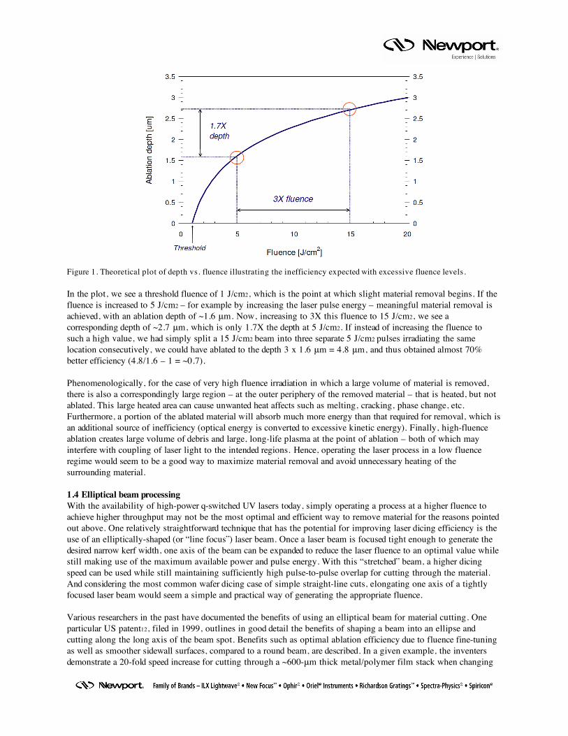
Figure 1. Theoretical plot of depth vs. fluence illustrating the inefficiency expected with excessive fluence levels. In the plot, we see a threshold fluence of 1 J/cm2, which is the point at which slight material removal begins. If the fluence is increased to 5 J/cm2 – for example by increasing the laser pulse energy – meaningful material removal is achieved, with an ablation depth of ~1.6 μm. Now, increasing to 3X this fluence to 15 J/cm2, we see a corresponding depth of ~2.7 μm, which is only 1.7X the depth at 5 J/cm2. If instead of increasing the fluence to such a high value, we had simply split a 15 J/cm2 beam into three separate 5 J/cm2 pulses irradiating the same location consecutively, we could have ablated to the depth 3 x 1.6 μm = 4.8 μm, and thus obtained almost 70% better efficiency (4.8/1.6 – 1 = ~0.7). Phenomenologically, for the case of very high fluence irradiation in which a large volume of material is removed, there is also a correspondingly large region – at the outer periphery of the removed material – that is heated, but not ablated. This large heated area can cause unwanted heat affects such as melting, cracking, phase change, etc. Furthermore, a portion of the ablated material will absorb much more energy than that required for removal, which is an additional source of inefficiency (optical energy is converted to excessive kinetic energy). Finally, high-fluence ablation creates large volume of debris and large, long-life plasma at the point of ablation – both of which may interfere with coupling of laser light to the intended regions. Hence, operating the laser process in a low fluence regime would seem to be a good way to maximize material removal and avoid unnecessary heating of the surrounding material. 1.4 Elliptical beam processing With the availability of high-power q-switched UV lasers today, simply operating a process at a higher fluence to achieve higher throughput may not be the most optimal and efficient way to remove material for the reasons pointed out above. One relatively straightforward technique that has the potential for improving laser dicing efficiency is the use of an elliptically-shaped (or “line focus”) laser beam. Once a laser beam is focused tight enough to generate the desired narrow kerf width, one axis of the beam can be expanded to reduce the laser fluence to an optimal value while still making use of the maximum available power and pulse energy. With this “stretched” beam, a higher dicing speed can be used while still maintaining sufficiently high pulse-to-pulse overlap for cutting through the material. And considering the most common wafer dicing case of simple straight-line cuts, elongating one axis of a tightly focused laser beam would seem a simple and practical way of generating the appropriate fluence. Various researchers in the past have documented the benefits of using an elliptical beam for material cutting. One particular US patent12, filed in 1999, outlines in good detail the benefits of shaping a beam into an ellipse and cutting along the long axis of the beam spot. Benefits such as optimal ablation efficiency due to fluence fine-tuning as well as smoother sidewall surfaces, compared to a round beam, are described. In a given example, the inventers demonstrate a 20-fold speed increase for cutting through a ~600-μm thick metal/polymer film stack when changing
from a round- to an elliptical-beam process. They also provide some results for elliptical beam cutting of silicon and gallium arsenide wafers; however they do not include comparative data for round-beam processing of these materials. Various other patents13, 14 have also touched upon certain benefits of processing with a non-round beam, as well as detailing various techniques for generating them. More recently, Migliore has shown15 what can be accomplished with higher-power 355nm q-switched laser sources available on the marketplace. When processing with multiple overlapping scans at high scan speeds, it was found that using an elliptical vs. a round beam increased the cutting speed for 100-μm thick silicon from 83 to 167 mm/s. 1.5 Pulse width considerations A very common answer to the question of what is the best laser pulse duration for a particular laser process is often: “It depends.” A longer pulse width will allow energy/heat to penetrate deeper into the material during the time of irradiation, and thus will generally remove more material per-pulse compared to shorter pulse widths. The extent of heating (thermal diffusion length) – and therefore the extent of material removal – increases with the square-root of the pulse duration. For example, a pulse duration of ~40 ns vs. 10 ns is expected to thermally penetrate twice as deep during the time of irradiation by the pulse. Indeed, for 355nm ns-pulse silicon machining, research has shown that longer pulses tend to exhibit a depth advantage for silicon machining16. Shorter pulse machining of silicon, however, is not without its own advantages. Generally, shorter pulse widths correspond to lower material ablation thresholds, which can have significant implications. Recent research17 has shown that shorter pulses can lead to quality benefits, including a reduction in heat affected zone (HAZ) generated in silicon. With a shorter pulse, reduced material heating can come in two ways: (1) reduced thermal diffusion length due to reduced time of irradiation of the material, and (2) less overall fluence required and applied due to a lower material removal threshold for short vs. long pulses. In the context of wafer dicing, the extended heating by a longer pulse laser would be expected to result in weaker singulated die (see Ref. 9) and a higher chance of thermal damage to circuit components on the die. From an efficiency standpoint, short-pulse machining at first glance is expected to be at a disadvantage due to the shallower thermal penetration and hence lower per-pulse removal rates. However, the aforementioned lower material removal threshold for shorter pulses should also be considered. Based on thermal diffusivity arguments, this threshold reduction scales with the square-root of the pulse duration. So, a pulse width of 10ns vs. 40-ns is expected to have a ~50% lower fluence threshold for material removal. Note that this counters the 2-fold depth increase previously described in above paragraph for the longer- vs. shorter-pulse. And so, considering the ability to operate at lower fluences due to a lower material removal threshold, there is ample reason to believe that a fluence-optimized short-pulse process can achieve very high material removal rates, while still maintaining the quality benefits of a more gentle, lower intensity process.
2. EXPERIMENT DETAILS In this work, we have characterized the relationship between silicon cutting speed and beam ellipticity for a short pulse width diode pumped solid state (DPSS) q-switched 355nm laser system. The emphasis is on thin (<100μm) silicon since that is where laser processing shows the most promise. The material used for all tests was 2” diameter, ~100-μm thick double-side polished single-crystal (<100>) silicon wafers. The principal goal of the experiment was to characterize the processing benefits that can be obtained for a silicon cutting process by stretching the major-axis (which is parallel to the cutting direction) of an elliptical Gaussian beam spot while keeping the minor-axis beam diameter at a fixed value, and using a constant pulse energy and pulse repetition frequency. 2.1 Laser system Spectra-Physics’ Pulseo® 355-20 high-power DPSS q-switched laser system was used for all results presented here. The laser is optimized for 100kHz performance and generates >20W for 200uJ pulse energy output with short, sub-23ns pulse durations. A detailed list of specifications for this system is in Table 1. Table 1. Specifications of Spectra Physics’ Pulseo® 355-20 laser system.
Parameter Value Wavelength 355 nm
Average Power >20 W Repetition Rate, nominal 100 kHz Repetition Rate Range 1 Hz–300 kHz Pulse Width <23 ns M2 <1.3 Beam Diameter, at waist 3.5 mm ±10% Pulse-to-Pulse Stability <5% rms 1σ
The Pulseo® is one of Spectra-Physics’ latest solid state q-switched laser systems for high-power UV industrial micromachining applications. 2.2 Optical set-up The optical set-up used for the experiments consists of a scanning galvanometer system (Scanlab Hurryscan II 10) with a 100mm focal length telecentric f-theta lens. The scan head is integrated into a precision linear motor XYZ positioning system (Newport Corporation IMS series stages and XPS motion controller) for full flexibility with regard to parts positioning and beam focusing capabilities. The Pulseo® laser beam was expanded by a factor of 2.5 to optimally fill the 10-mm scan head aperture. Prior to introducing beam ellipticity, the combination of focusing an M2 = 1.3 laser beam with 100mm focal length lens after 2.5X beam expansion results (theoretically) in a round-beam focus diameter (1/e2) of ~9 μm. To generate a line focus, a pair of cylindrical lenses (+/- 100 mm focal length) was inserted into the beam path just before the galvo scanner aperture. By varying the separation distance between these lenses, the amount of beam ellipticity at the focal plane of the f-theta lens can be adjusted; that is, with the target material fixed at the focal plane of the 100mm FL f-theta lens, the major axis is varied while the minor-axis is fixed at ~9 μm. Beam ellipticity is defined here as the major axis beam diameter (at 1/e2 intensity) divided by the minor axis beam diameter, and is therefore always greater than one. 2.3 Experimental procedures Preliminary tests were performed and consisted of varying both the beam scanning speed and the number of overlapping scans in order to determine the best combination for clean and efficient cutting of the silicon. Using the galvo scanner system, it is possible to scan at several meters per second; and the precision is reasonably sufficient for overlapping the scans atop one another on the material. For such a high-speed, multi-pass process, the relevant quantity from a process efficiency point of view is the scan speed divided by the number of scans, and is referred to as the average, net, or effective cutting speed. In general, but especially with higher-fluence processing, it is often advantageous to use such a high-speed, multi-pass process. This can lead to better quality cuts, since there is less heating/melting/cracking compared to slower speeds, and higher processing speeds, as well, since there is less debris- and plasma-shielding of the incoming laser pulses. Using full power output of the laser beam at the system-optimal 100kHz pulse repetition frequency, the galvo scanner was used to scan the focused beam, in the direction parallel to the long-axis of the ellipse, across a nominally 100-μm thick single crystal <100> silicon wafer. Both the scanning speed and, in some cases, the number of scans were varied for a given scan routine. Upon the completion of the scan routine, the spacing of the cylindrical lens pair was increased to create a longer major axis, while maintaining the same minor-axis beam width of ~9 μm. The scan routine was then repeated with the adjusted line-focus beam. All processing was performed in normal air-atmosphere ambient environment. Table 2 contains a listing of the relevant parameters and their values / ranges used to generate the results presented here. Table 2. Summary of process parameter values and ranges used for the tests.
Parameter Value or range Power, on target 18 W PRF: 100 kHz Pulse energy 180 µJ Minor axis beam diam. 9 µm Major axis beam diam. 170 – 930 µm Ellipticity, major/minor ~20 – 100 Scan speed 200 – 1500
mm/s Number of scans 1 – 4
Once a sufficient parameter space was explored, the samples were inspected. Initially, inspection consisted of optical surface microscopy using reflected and transmitted light to check for kerf width and cut-through of the material. With this basic technique, it was possible to determine the range of parameters for which 100-μm thick silicon could be fully cut. However, to obtain depth information for laser scribes less than 100-μm deep, it was necessary to cleave the samples for cross-sectional examination. The appropriate samples were prepared and cleaved along the laser scribe, thus exposing the laser-scribed region for measurement with the optical microscope. In this manner, a complete set of laser cutting depth data was generated for a range of speeds and a range of beam ellipticities. Additional data on the sidewall surface roughness was generated using a scanning white light optical profiler system (Zygo NewView 7200).
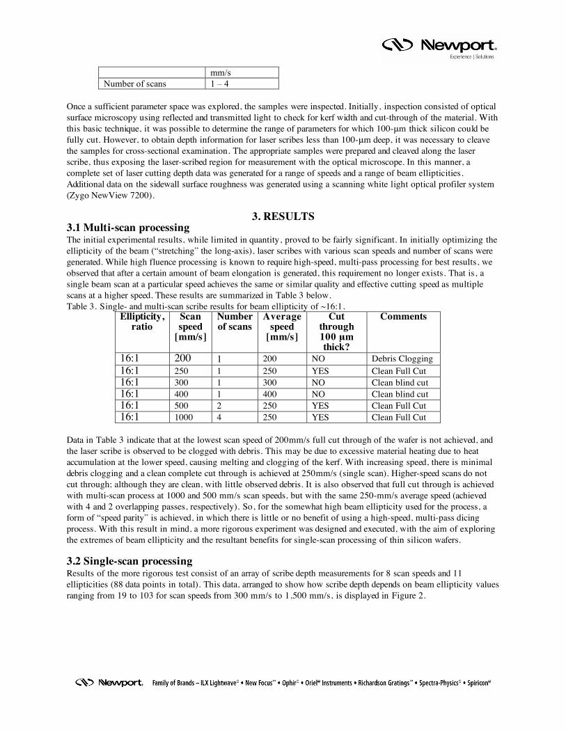
3. RESULTS 3.1 Multi-scan processing The initial experimental results, while limited in quantity, proved to be fairly significant. In initially optimizing the ellipticity of the beam (“stretching” the long-axis), laser scribes with various scan speeds and number of scans were generated. While high fluence processing is known to require high-speed, multi-pass processing for best results, we observed that after a certain amount of beam elongation is generated, this requirement no longer exists. That is, a single beam scan at a particular speed achieves the same or similar quality and effective cutting speed as multiple scans at a higher speed. These results are summarized in Table 3 below. Table 3. Single- and multi-scan scribe results for beam ellipticity of ~16:1.
Ellipticity, ratio
Scan speed
[mm/s]
Number of scans
Average speed
[mm/s]
Cut through 100 μm thick?
Comments
16:1 200 1 200 NO Debris Clogging 16:1 250 1 250 YES Clean Full Cut 16:1 300 1 300 NO Clean blind cut 16:1 400 1 400 NO Clean blind cut 16:1 500 2 250 YES Clean Full Cut 16:1 1000 4 250 YES Clean Full Cut
Data in Table 3 indicate that at the lowest scan speed of 200mm/s full cut through of the wafer is not achieved, and the laser scribe is observed to be clogged with debris. This may be due to excessive material heating due to heat accumulation at the lower speed, causing melting and clogging of the kerf. With increasing speed, there is minimal debris clogging and a clean complete cut through is achieved at 250mm/s (single scan). Higher-speed scans do not cut through; although they are clean, with little observed debris. It is also observed that full cut through is achieved with multi-scan process at 1000 and 500 mm/s scan speeds, but with the same 250-mm/s average speed (achieved with 4 and 2 overlapping passes, respectively). So, for the somewhat high beam ellipticity used for the process, a form of “speed parity” is achieved, in which there is little or no benefit of using a high-speed, multi-pass dicing process. With this result in mind, a more rigorous experiment was designed and executed, with the aim of exploring the extremes of beam ellipticity and the resultant benefits for single-scan processing of thin silicon wafers. 3.2 Single-scan processing Results of the more rigorous test consist of an array of scribe depth measurements for 8 scan speeds and 11 ellipticities (88 data points in total). This data, arranged to show how scribe depth depends on beam ellipticity values ranging from 19 to 103 for scan speeds from 300 mm/s to 1,500 mm/s, is displayed in Figure 2.
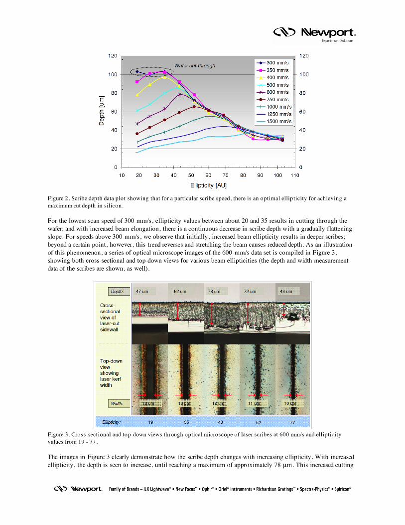
Figure 2. Scribe depth data plot showing that for a particular scribe speed, there is an optimal ellipticity for achieving a maximum cut depth in silicon. For the lowest scan speed of 300 mm/s, ellipticity values between about 20 and 35 results in cutting through the wafer; and with increased beam elongation, there is a continuous decrease in scribe depth with a gradually flattening slope. For speeds above 300 mm/s, we observe that initially, increased beam ellipticity results in deeper scribes; beyond a certain point, however, this trend reverses and stretching the beam causes reduced depth. As an illustration of this phenomenon, a series of optical microscope images of the 600-mm/s data set is compiled in Figure 3, showing both cross-sectional and top-down views for various beam ellipticities (the depth and width measurement data of the scribes are shown, as well).
Figure 3. Cross-sectional and top-down views through optical microscope of laser scribes at 600 mm/s and ellipticity values from 19 - 77. The images in Figure 3 clearly demonstrate how the scribe depth changes with increasing ellipticity. With increased ellipticity, the depth is seen to increase, until reaching a maximum of approximately 78 μm. This increased cutting

depth is accompanied by a narrowing of the kerf width, which is particularly advantageous for processing wafers having narrow dicing streets. This phenomenon is inherent to Gaussian beam machining and is a result of a narrower region of the Gaussian beam intensity distribution (along the minor-axis) being above the material’s ablation threshold. Further stretching of the beam causes a continued reduction in cutting depth, as well as increased irregularity to the scribe floor. The data have shown that for each scan speed tested there is a maximum machining depth that is achieved; and this depth occurs at a well-defined optimal beam ellipticity. For a given ellipticity, there is a representative average fluence value that may be defined as: o(maj ) o(min) p avg w w E F p = , where Ep is the laser pulse energy, and wo(maj) and wo(min) are the 1/e2 beam radii of the major and minor beam axes, respectively, of the elliptical beam spot. These two quantities – the maximum cutting depth for a particular speed and the average fluence at which this depth is achieved – are graphically displayed in Figure 4.
Figure 4. Optimized cutting depth, and fluence at which this depth is achieved, versus scan speed. The data for maximum depth vs. cutting speed fits nicely to a logarithmic trend line, as does the curve for optimal fluence at each cutting speed. This data shows the clear trending of cutting depth into a speed regime of meters per second. Also, it is evident that shallower cutting depths require lower fluences at the condition of optimal ellipticity. 3.3 Surface finish quality Optical profilometry was also used to inspect and analyze the sidewalls of some scribes generated in the tests. Since smoother sidewalls and minimal chipping are believed to result in improved die strength19, this is an important aspect of any dicing process. Figure 5 below shows a 3-dimension optical profile image as well as roughness measurement data that were generated for a ~97-μm deep scribe machined at 400mm/s scan speed with a beam ellipticity of ~35:1.
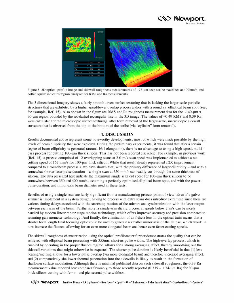
Figure 5. 3D optical profile image and sidewall roughness measurements of ~97-μm deep scribe machined at 400mm/s; red dotted square indicates region analyzed for RMS and Ra measurements. The 3-dimensional imagery shows a fairly smooth, even surface texturing that is lacking the larger-scale periodic structures that are exhibited by a higher speed/lower overlap process and/or with a round vs. elliptical beam spot (see, for example, Ref. 15). Also shown in the figure are RMS and Ra roughness measurement data for the ~140-μm x 90-μm region bounded by the red-dashed rectangular line in the 3D image. The values of ~0.49 RMS and 0.39 Ra were calculated for the microscopic surface texturing, after form removal of the larger-scale, macroscopic sidewall curvature that is observed from the top to the bottom of the scribe (via “cylinder” form removal).
4. DISCUSSION Results documented above represent some noteworthy developments, most of which were made possible by the high levels of beam ellipticity that were explored. During the preliminary experiments, it was found that after a certain degree of beam ellipticity is generated (around 16:1 elongation), there is no advantage to using a high-speed, multi-pass process for cutting 100-μm thick silicon. This has not been reported elsewhere. For example, in previous work (Ref. 15), a process comprised of 12 overlapping scans at 2.0 m/s scan speed was implemented to achieve a net cutting speed of 167 mm/s for 100-μm thick silicon. While that result already represented a 2X improvement compared to a roundbeam process18, we have shown that, with the primary difference of larger ellipticity – and with a somewhat shorter laser pulse duration – a single scan at 350-mm/s can readily cut through the same thickness of silicon. The data presented here indicate the maximum single scan cut speed for 100-μm thick silicon to be somewhere between 350 and 400 mm/s, assuming a perfectly optimized elliptical beam spot, and with the power, pulse duration, and minor-axis beam diameter used in these tests. Benefits of using a single scan are fairly significant from a manufacturing process point of view. Even if a galvo scanner is implement in a system design, having to process with extra scans does introduce extra time since there are various timing delays associated with the start/stop motion of the mirrors and synchronization with the laser output between each scan of the beam. Furthermore, a single-scan dicing process at speeds below 2 m/s can be nicely handled by modern linear motor stage motion technology, which offers improved accuracy and precision compared to scanning galvanometer technology. And finally, the elimination of an f-theta lens in the optical train means that a shorter focal length final focusing optic could be used to generate a smaller minor axis of the ellipse, which would in turn increase the fluence, allowing for an even more elongated beam and hence even faster cutting speeds. The sidewall roughness characterization using the optical profilometer further demonstrates the quality that can be achieved with elliptical beam processing with 355nm, short-ns pulse widths. The high-overlap process, which is enabled by operating in the proper fluence regime, allows for a strong averaging affect, thereby smoothing out the sidewall variations that might otherwise be expected. The shorter pulse duration is likely beneficial in that (1) less heating/melting allows for a lower pulse overlap (via more elongated beam) and therefore increased averaging affect, and (2) comparatively shallower thermal penetration into the sidewalls is likely to result in the formation of shallower surface modulation. Although there is minimal published data on such sidewall roughness, the 0.39 Ra measurement value reported here compares favorably to those recently reported (0.335 – 1.74-μm Ra) for 80-μm thick silicon cutting with femto- and picosecond pulse widths20.
For the laser power / pulse energy used, and for the ~9-μm minor axis beam diameter, it is apparent that optimization of the beam ellipticity resulted in the determination of the fastest silicon cutting speed for the various cutting thicknesses of interest. Clearly, for each speed tested, there was a peak cutting depth that corresponded to a particular ellipticity (and hence fluence). For 100-μm thick wafers, speeds between 350 and 400 mm/s are possible; for 75-, and 50-μm thick silicon wafers, the results show that cutting speeds of 600 and 1000 mm/s, respectively, are easily achieved. Extrapolating the logarithmic curve fit to the data in Figure 4, laser-dicing of 25-μm thick wafers looks to be possible at speeds near 2000 mm/s when using the optimal beam ellipticity. An additional benefit to performing the line-focus fluence-optimization technique described here is that kerf width-narrowing is seen to occur as the ellipse is optimized for increased machining depth. This result, which is due to the thresholding effect of a Gaussian beam intensity distribution, is beneficial to machining the increasingly narrow dicing streets of current and future wafers. With decreasing thickness, the increased optimal ellipticity corresponds to a decreased optimal fluence. For scribe depths of just below 40 μm to just above 100 μm, the corresponding optimal average fluence value ranges from ~3 to ~9 J/cm2. This trending is to be expected, since cutting thicker materials will require higher fluence at the surface to overcome factors such as shadowing effects of deeper grooves and the depletion effects of sidewall absorption of laser energy as the light propagates down the laser-cut groove. This result nicely demonstrates that – even with wavelength, pulse width, etc. held constant – there is no single “best” fluence for cutting through silicon; rather the ideal fluence is dependent on the thickness of the material to be cut. In the logical extreme, in which the thickness of the wafer is similar to the thermal (or optical) penetration depth of the irradiating laser, the optimal fluence is exactly equal (or similar) to the ablation threshold itself.
5. CONCLUSIONS Using a line-focus, fluence optimization technique, highest-speed dicing of thin silicon wafers has been demonstrated. With a 9-μm minor axis beam diameter and 18 W laser power on-target, full-cut scan speed for 100-μm thick silicon wafers was found to be between 350 and 400 mm/s. To our knowledge, this is the fastest cutting speed demonstrated to date with a ns-pulse, 355-nm DPSS q-switched laser source. For a range of silicon thicknesses, the fastest cutting speed and optimal ellipticity for achieving this speed has been determined. Cutting >50-μm deep in silicon was achieved with 1-m/s scan speed; and an extrapolation of data trend line indicates 25-μm deep cuts could be made at ~2-m/s scan speed. An additional benefit to optimizing the beam ellipticity is that the kerf width becomes narrower while at the same time achieving deeper cutting, which make such a process even more suitable for current and future industrial wafer dicing needs. With ellipticities greater than about 16:1 ratio, it was found that high-speed, multi-pass beam scanning was not necessary to generate high-quality, high-throughput results. Rather, a single scan at the optimal fluence is found to give bestquality and best-efficiency results. This development is even more significant when considering the system advantages that potentially exist for using motion stages instead of scanning galvanometer systems for wafer dicing tools. Additionally, optical profilometry analysis indicates that the combination of high pulse overlap, large beam ellipticity, and short pulse width yielded very high-quality cuts with minimal sidewall roughness. These results further prove the advantage of laser dicing over conventional saw-dicing techniques for thin silicon wafers. Furthermore, they demonstrate that by optimizing the beam ellipticity for maximum cutting speed, both a high-quality and a high-throughput process can be realized with a short ns-pulse, 355nm q-switched DPSS laser source. REFERENCES [1] Dunsky, C.M., “Laser material processing in microelectronics manufacturing: status and near-term opportunities,” Proc. SPIE 5713, 200-214 (2005). [2] Zeng, X.J., Mao, X., Greif, R., Russo, R.E., “Ultravoilet femtosecond and nanosecond laser ablation of silicon: ablation efficiency and laser-induced plasma expansion,” Proc. SPIE 5448, 1150-1158 (2004).
[3] Lim, G.C., Tuan, A.M., Low, D., Chen, Q., “High quality laser microcutting of difficult-to-cut materials – copper and silicon wafer,” Proc. ICALEO 2002, Scottsdale (2002). [4] Corboline, T., Hoult., A.P., “Laser machining of silicon using diode-pumped solid state & CO2 lasers,” Proc. ICALEO 2002, Scottsdale (2002). [5] Bonse, J., Baudach, S., Kruger, J., Kautek, W., Lenzner, M., “Femtosecond laser ablation of silicon – modification thresholds and morphology,” App. Phys. A 74, 19-25 (2002). [6] Raciukaitis, G., Brikas, M., “Micro-machining of silicon and glass with picosecond lasers,” Proc. SPIE 5662, 717- 721 (2004). [7] Klotzbach, U., Panzner, M., Kasper, J., Hendrik, W., Thomas, K., Franke, V., Eckhard, B., “Processing of silicon by Nd:YAG-lasers with harmonics generation,” Proc. ICALEO 2002, Scottsdale (2002). [8] US Patent 6,992,026, Hamamatsu Photonics K.K. (2006). [9] Haupt, O., Siegel, F., Schoonderbeek, A., Richter, L., Kling, R., Ostendorf, A., “Laser dicing of silicon: comparison of ablation mechanisms with a novel technology of thermally induced stress,” Proc. Of LMP2008, Quebec (2008). [10] Shimizu, K., Takahashi, K., Morikazu, H., Ogoshi, N., Takeyama, K., Wakayama, Y., Obara, T., “Laser ablation with water micro-drop for dicing of silicon wafer,” Proc. ICALEO 2004, San Francisco, (2004). [11] Dushkina, N.M., Wagner, F.R., Boillat, C., Buchilly, J-M., Richerzhagen, B., “Water jet guided laser versus saw dicing,” Proc. SPIE 4977, 75-85 (2003). [12] US Patent 6,472,295, JMAR Research, Inc. (2002). [13] US Patent 6,989,508, GSI Group Corp. (2006). [14] US Patent 7,388,172, J.P. Sercel Associates, Inc. (2008). [15] Migliore, L., “Enhancing silicon cutting performance by shaping the focused beam,” Proc. SPIE 6458, 1-9 (2007). [16] Li, M., “Effect of laser parameters on semiconductor micromachining using diode-pumped solid-state lasers,” Proc. ICALEO 2003, Jacksonville (2003). [17] Pantsar, H., Herfurth, H., Heinemann, S., Laakso, P., Penttila, R., Liu, Y., Newaz, G., “Laser microvia drilling and ablation of silicon using 355 nm pico and nanosecond pulses,” Proc. ICALEO 2008, Temecula (2008). [18] Toftness, R.F., Boyle, A., Gillen, D., “Laser technology for wafer dicing and microvia drilling for next generation wafers,” Proc. SPIE 5713, 54-66 (2005). [19] Schoenfelder, S., Ebert, M., Landesberger, C., Bock, K., Bagdahn, J., “Investigations of the influence of dicing techniques on the strength properties of thin silicon,” Microelectronics Reliability 47, 168-178 (2007). [20] Sudani, N., Venkatakrishnan, K., Tan, B., “Laser singulation of thin wafer: die strength and surface roughness analysis of 80 µm silicon dice,” Optics and Lasers in Engineering v. 47, 850-854 (2009).