
High Linearity SP2T Wi-Fi RF Switch 100MHz to 8GHz
19
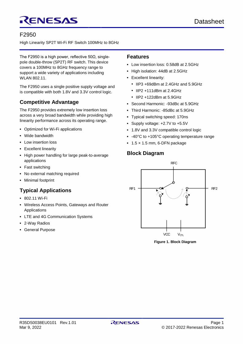
Datasheet F2950 High Linearity SP2T Wi-Fi RF Switch 100MHz to 8GHz R35DS0038EU0101 Rev.1.01 Mar 9, 2022 Page 1 © 2017-2022 Renesas Electronics The F2950 is a high power, reflective 50Ω, single- pole double-throw (SP2T) RF switch. This device covers a 100MHz to 8GHz frequency range to support a wide variety of applications including WLAN 802.11. The F2950 uses a single positive supply voltage and is compatible with both 1.8V and 3.3V control logic. Competitive Advantage The F2950 provides extremely low insertion loss across a very broad bandwidth while providing high linearity performance across its operating range. ■ Optimized for Wi-Fi applications ■ Wide bandwidth ■ Low insertion loss ■ Excellent linearity ■ High power handling for large peak-to-average applications ■ Fast switching ■ No external matching required ■ Minimal footprint Typical Applications ■ 802.11 Wi-Fi ■ Wireless Access Points, Gateways and Router Applications ■ LTE and 4G Communication Systems ■ 2-Way Radios ■ General Purpose Features ■ Low insertion loss: 0.58dB at 2.5GHz ■ High isolation: 44dB at 2.5GHz ■ Excellent linearity: ● IIP3 +69dBm at 2.4GHz and 5.9GHz ● IIP2 +111dBm at 2.4GHz ● IIP2 +122dBm at 5.9GHz ■ Second Harmonic: -93dBc at 5.9GHz ■ Third Harmonic: -85dBc at 5.9GHz ■ Typical switching speed: 170ns ■ Supply voltage: +2.7V to +5.5V ■ 1.8V and 3.3V compatible control logic ■ -40°C to +105°C operating temperature range ■ 1.5 × 1.5 mm, 6-DFN package Block Diagram Figure 1. Block Diagram RF2 RF1 RFC V CTL VCC
Transcript of High Linearity SP2T Wi-Fi RF Switch 100MHz to 8GHz
Datasheet
F2950 High Linearity SP2T Wi-Fi RF Switch 100MHz to 8GHz
R35DS0038EU0101 Rev.1.01 Mar 9, 2022
Page 1 © 2017-2022 Renesas Electronics
The F2950 is a high power, reflective 50Ω, single-pole double-throw (SP2T) RF switch. This device covers a 100MHz to 8GHz frequency range to support a wide variety of applications including WLAN 802.11.
The F2950 uses a single positive supply voltage and is compatible with both 1.8V and 3.3V control logic.
Competitive Advantage The F2950 provides extremely low insertion loss across a very broad bandwidth while providing high linearity performance across its operating range.
Optimized for Wi-Fi applications Wide bandwidth Low insertion loss Excellent linearity High power handling for large peak-to-average
applications Fast switching No external matching required Minimal footprint
Typical Applications 802.11 Wi-Fi Wireless Access Points, Gateways and Router
Applications LTE and 4G Communication Systems 2-Way Radios General Purpose
Features Low insertion loss: 0.58dB at 2.5GHz High isolation: 44dB at 2.5GHz Excellent linearity:
IIP3 +69dBm at 2.4GHz and 5.9GHz IIP2 +111dBm at 2.4GHz IIP2 +122dBm at 5.9GHz
Second Harmonic: -93dBc at 5.9GHz Third Harmonic: -85dBc at 5.9GHz Typical switching speed: 170ns Supply voltage: +2.7V to +5.5V 1.8V and 3.3V compatible control logic -40°C to +105°C operating temperature range 1.5 × 1.5 mm, 6-DFN package
Block Diagram
Figure 1. Block Diagram
RF2RF1
RFC
VCTLVCC
F2950 Datasheet
R35DS0038EU0101 Rev.1.01 Mar 9, 2022
Page 2
Contents 1. Pin Information ............................................................................................................................................. 3
1.1 Pin Assignments ................................................................................................................................... 3 1.2 Pin Descriptions .................................................................................................................................... 3
2. Specifications ............................................................................................................................................... 4 2.1 Absolute Maximum Ratings .................................................................................................................. 4 2.2 ESD Ratings ......................................................................................................................................... 4 2.3 Recommended Operating Conditions ................................................................................................... 5 2.4 Thermal Specifications ......................................................................................................................... 5 2.5 Electrical Specifications ........................................................................................................................ 6
3. Typical Operating Conditions (TOCs) ......................................................................................................... 8
4. Typical Performance Characteristics [1] .................................................................................................... 9
5. Typical Performance Characteristics [2] .................................................................................................. 10
6. Typical Performance Characteristics [3] .................................................................................................. 11
7. Control Mode .............................................................................................................................................. 12
8. Application Information ............................................................................................................................. 12 8.1 Default Start-up .................................................................................................................................. 12 8.2 Power Supplies ................................................................................................................................... 12 8.3 Control Pin Interface ........................................................................................................................... 12
9. Evaluation Kit .............................................................................................................................................. 13 9.1 Evaluation Kit Picture.......................................................................................................................... 13 9.2 Evaluation Kit / Applications Circuit .................................................................................................... 14 9.3 Evaluation Kit (EVKit) Operation ......................................................................................................... 15
9.3.1. External Supply Setup .......................................................................................................... 15 9.3.2. Logic Control Setup .............................................................................................................. 15 9.3.3. Turn On Procedure ............................................................................................................... 15 9.3.4. Turn Off Procedure ............................................................................................................... 15
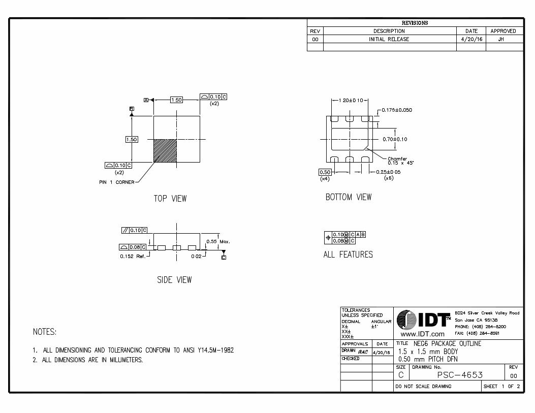
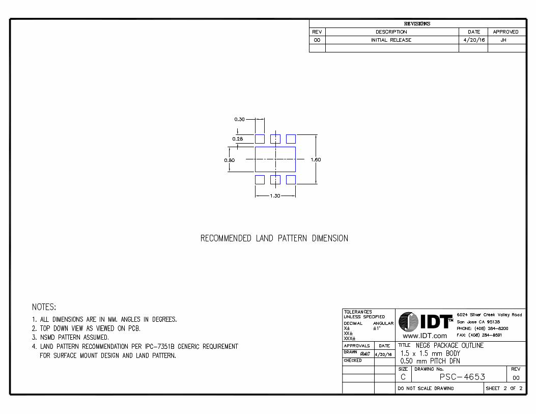
10. Package Outline Drawings ......................................................................................................................... 16
11. Marking Diagram ........................................................................................................................................ 16
12. Ordering Information .................................................................................................................................. 16
13. Revision History ......................................................................................................................................... 16
F2950 Datasheet
R35DS0038EU0101 Rev.1.01 Mar 9, 2022
Page 3
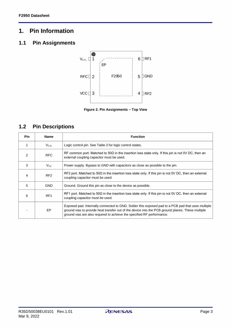
1. Pin Information
1.1 Pin Assignments
RF2
VCTL
GND
RF1
VCC
F2950
1
2
3
6
5
4
EP
RFC
Figure 2. Pin Assignments – Top View
1.2 Pin Descriptions
Pin Name Function
1 VCTL Logic control pin. See Table 3 for logic control states.
2 RFC RF common port. Matched to 50Ω in the insertion loss state only. If this pin is not 0V DC, then an external coupling capacitor must be used.
3 VCC Power supply. Bypass to GND with capacitors as close as possible to the pin.
4 RF2 RF2 port. Matched to 50Ω in the insertion loss state only. If this pin is not 0V DC, then an external coupling capacitor must be used.
5 GND Ground. Ground this pin as close to the device as possible.
6 RF1 RF1 port. Matched to 50Ω in the insertion loss state only. If this pin is not 0V DC, then an external coupling capacitor must be used.
- EP Exposed pad. Internally connected to GND. Solder this exposed pad to a PCB pad that uses multiple ground vias to provide heat transfer out of the device into the PCB ground planes. These multiple ground vias are also required to achieve the specified RF performance.
F2950 Datasheet
R35DS0038EU0101 Rev.1.01 Mar 9, 2022
Page 4
2. Specifications
2.1 Absolute Maximum Ratings Stresses beyond those listed below may cause permanent damage to the device. Functional operation of the device at these or any other conditions beyond those indicated in the operational section of this specification is not implied. Exposure to absolute maximum rating conditions for extended periods may affect device reliability.
Parameter Symbol Minimum Maximum Unit
VCC to GND VCC -0.3 +6.0 V
VCTL to GND VLOGIC -0.3 Lower of
(VCC + 0.3, 3.9) V
RF1, RF2, RFC to GND VRF -0.3 +0.3 V
Maximum Input CW Power, ZS = ZL = 50Ω, TEP = 25°C, VCC = 5.25V (any port, insertion loss state) [1]
100MHz ≤ fRF ≤ 200MHz PABSCW1 - 28
dBm
200MHz < fRF ≤ 500MHz PABSCW2
- 29
500MHz < fRF ≤ 1GHz PABSCW3 - 30
1GHz < fRF ≤ 6GHz PABSCW4 - 31
fRF > 6GHz PABSCW5 - 30
Maximum Peak Power, ZS = ZL = 50Ω, TEP = 25°C, VCC = 5.25V (any port, insertion loss state) [1] [2]
100MHz ≤ fRF ≤ 200MHz PABSPK1
- 35
dBm
200MHz < fRF ≤ 500MHz PABSPK2
- 36
500MHz < fRF ≤ 1GHz PABSPK3 - 37
1GHz < fRF ≤ 6GHz PABSPK4 - 38
fRF > 6GHz PABSPK5 - 37
Maximum Junction Temperature TJMAX - - °C
Storage Temperature Range TSTOR -65 +150 °C
Lead Temperature (soldering, 10s) TLEAD - +260 °C
1. TEP is the temperature of the exposed paddle. 2. 5% duty cycle of 4.6ms period in a 50Ω environment.
2.2 ESD Ratings
ESD Model/Test Symbol Rating Unit
Electrostatic Discharge – HBM (JEDEC/ESDA JS-001-2012) VESDHBM 2000 (Class C2) V
Electrostatic Discharge – CDM (JEDEC 22-C101F) VESDCDM 500 (Class C2) V
F2950 Datasheet
R35DS0038EU0101 Rev.1.01 Mar 9, 2022
Page 5
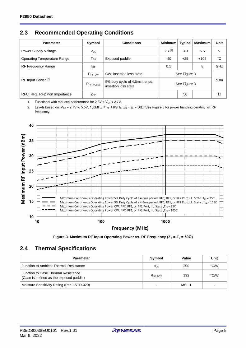
2.3 Recommended Operating Conditions
Parameter Symbol Conditions Minimum Typical Maximum Unit
Power Supply Voltage VCC 2.7 [1] 3.3 5.5 V
Operating Temperature Range TEP Exposed paddle -40 +25 +105 °C
RF Frequency Range fRF 0.1 8 GHz
RF Input Power [2]
PRF_CW CW, insertion loss state See Figure 3
dBm PRF_PULSE 5% duty cycle of 4.6ms period,
insertion loss state See Figure 3
RFC, RF1, RF2 Port Impedance ZRF 50 Ω
1. Functional with reduced performance for 2.3V ≤ VCC < 2.7V. 2. Levels based on: VCC = 2.7V to 5.5V, 100MHz ≤ fRF ≤ 8GHz, ZS = ZL = 50Ω. See Figure 3 for power handling derating vs. RF
frequency.
Figure 3. Maximum RF Input Operating Power vs. RF Frequency (ZS = ZL = 50Ω)
2.4 Thermal Specifications
Parameter Symbol Value Unit
Junction to Ambient Thermal Resistance θJA 200 °C/W
Junction to Case Thermal Resistance (Case is defined as the exposed paddle) θJC_BOT 132 °C/W
Moisture Sensitivity Rating (Per J-STD-020) - MSL 1 -
F2950 Datasheet
R35DS0038EU0101 Rev.1.01 Mar 9, 2022
Page 6
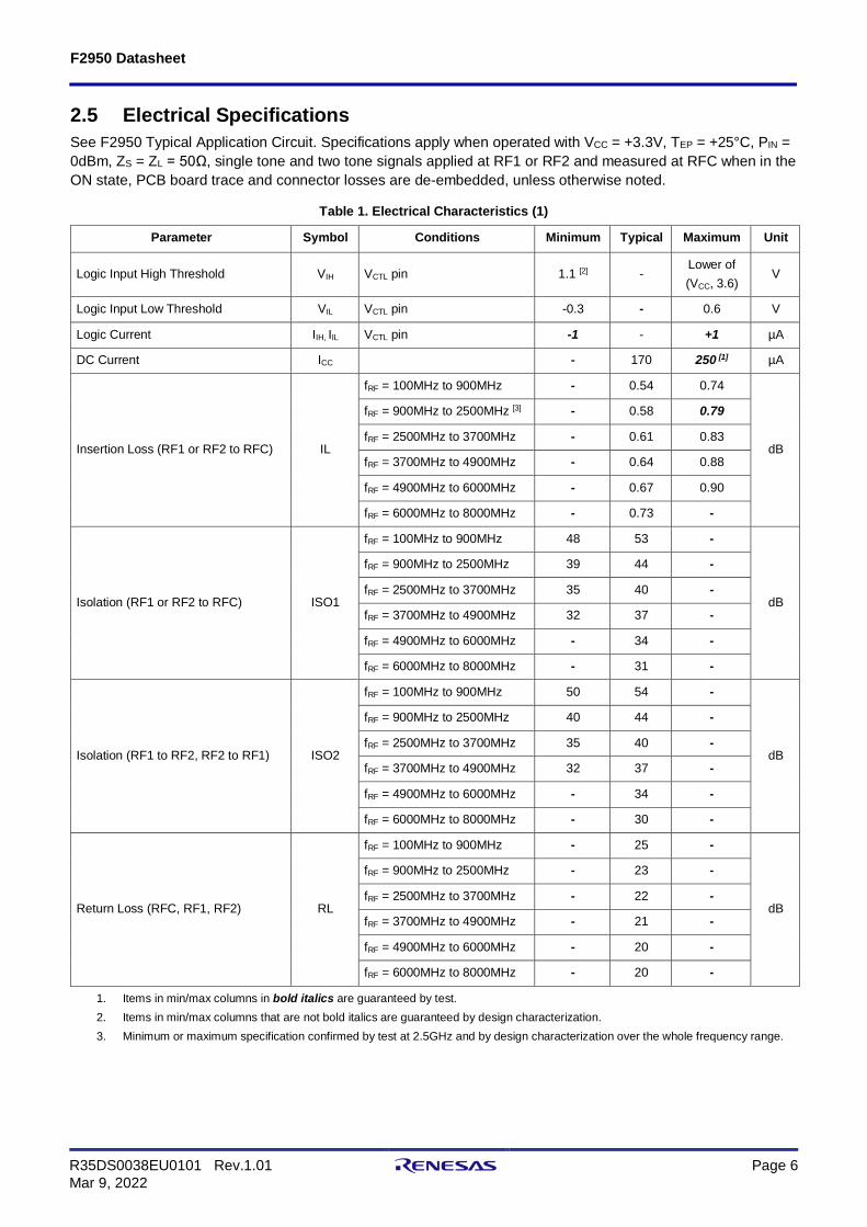
2.5 Electrical Specifications See F2950 Typical Application Circuit. Specifications apply when operated with VCC = +3.3V, TEP = +25°C, PIN = 0dBm, ZS = ZL = 50Ω, single tone and two tone signals applied at RF1 or RF2 and measured at RFC when in the ON state, PCB board trace and connector losses are de-embedded, unless otherwise noted.
Table 1. Electrical Characteristics (1)
Parameter Symbol Conditions Minimum Typical Maximum Unit
Logic Input High Threshold VIH VCTL pin 1.1 [2] - Lower of (VCC, 3.6)
V
Logic Input Low Threshold VIL VCTL pin -0.3 - 0.6 V
Logic Current IIH, IIL VCTL pin -1 - +1 µA
DC Current ICC - 170 250 [1] µA
Insertion Loss (RF1 or RF2 to RFC) IL
fRF = 100MHz to 900MHz - 0.54 0.74
dB
fRF = 900MHz to 2500MHz [3] - 0.58 0.79
fRF = 2500MHz to 3700MHz - 0.61 0.83
fRF = 3700MHz to 4900MHz - 0.64 0.88
fRF = 4900MHz to 6000MHz - 0.67 0.90
fRF = 6000MHz to 8000MHz - 0.73 -
Isolation (RF1 or RF2 to RFC) ISO1
fRF = 100MHz to 900MHz 48 53 -
dB
fRF = 900MHz to 2500MHz 39 44 -
fRF = 2500MHz to 3700MHz 35 40 -
fRF = 3700MHz to 4900MHz 32 37 -
fRF = 4900MHz to 6000MHz - 34 -
fRF = 6000MHz to 8000MHz - 31 -
Isolation (RF1 to RF2, RF2 to RF1) ISO2
fRF = 100MHz to 900MHz 50 54 -
dB
fRF = 900MHz to 2500MHz 40 44 -
fRF = 2500MHz to 3700MHz 35 40 -
fRF = 3700MHz to 4900MHz 32 37 -
fRF = 4900MHz to 6000MHz - 34 -
fRF = 6000MHz to 8000MHz - 30 -
Return Loss (RFC, RF1, RF2) RL
fRF = 100MHz to 900MHz - 25 -
dB
fRF = 900MHz to 2500MHz - 23 -
fRF = 2500MHz to 3700MHz - 22 -
fRF = 3700MHz to 4900MHz - 21 -
fRF = 4900MHz to 6000MHz - 20 -
fRF = 6000MHz to 8000MHz - 20 -
1. Items in min/max columns in bold italics are guaranteed by test. 2. Items in min/max columns that are not bold italics are guaranteed by design characterization. 3. Minimum or maximum specification confirmed by test at 2.5GHz and by design characterization over the whole frequency range.
F2950 Datasheet
R35DS0038EU0101 Rev.1.01 Mar 9, 2022
Page 7
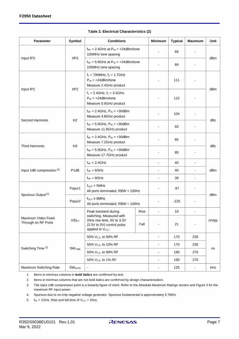
Table 2. Electrical Characteristics (2)
Parameter Symbol Conditions Minimum Typical Maximum Unit
Input IP3 IIP3
fRF = 2.4GHz at PIN = +24dBm/tone 100MHz tone spacing
- 69 -
dBm fRF = 5.9GHz at PIN = +24dBm/tone 100MHz tone spacing
- 69 -
Input IP2 IIP2
f1 = 700MHz, f2 = 1.7GHz PIN = +24dBm/tone Measure 2.4GHz product
- 111 -
dBm f1 = 2.4GHz, f2 = 3.5GHz PIN = +24dBm/tone Measure 5.9GHz product
- 122 -
Second Harmonic H2
fRF = 2.4GHz, PIN = +30dBm Measure 4.8GHz product
- 104 -
dBc fRF = 5.9GHz, PIN = +30dBm Measure 11.8GHz product
- 93 -
Third Harmonic H3
fRF = 2.4GHz, PIN = +30dBm Measure 7.2GHz product
- 85 -
dBc fRF = 5.9GHz, PIN = +30dBm Measure 17.7GHz product
- 85 -
Input 1dB compression [3] P1dB
fRF = 2.4GHz - 40 -
dBm fRF = 6GHz - 40 -
fRF = 8GHz - 39 -
Spurious Output [4]
Pspur1 fOUT > 5MHz All ports terminated, RBW = 100Hz
- -97 -
dBm
Pspur2 fOUT ≤ 5MHz All ports terminated, RBW = 100Hz
- -125 -
Maximum Video Feed-Through on RF Ports VIDFT
Peak transient during switching. Measured with 20ns rise time, 0V to 3.3V (3.3V to 0V) control pulse applied to VCTL.
Rise - 10 -
mVpp Fall - 21 -
Switching Time [5] SWTIME
50% VCTL to 90% RF - 170 230
ns 50% VCTL to 10% RF - 170 230
50% VCTL to 99% RF - 190 270
50% VCTL to 1% RF - 190 270
Maximum Switching Rate SWRATE - - 125 - kHz
1. Items in min/max columns in bold italics are confirmed by test. 2. Items in min/max columns that are not bold italics are confirmed by design characterization. 3. The input 1dB compression point is a linearity figure of merit. Refer to the Absolute Maximum Ratings section and Figure 3 for the
maximum RF input power. 4. Spurious due to on-chip negative voltage generator. Spurious fundamental is approximately 5.7MHz. 5. fRF = 1GHz. Rise and fall time of VCTL = 20ns.
F2950 Datasheet
R35DS0038EU0101 Rev.1.01 Mar 9, 2022
Page 8
3. Typical Operating Conditions (TOCs) Unless otherwise noted:
VCC = +3.3V TEP = 25°C ZS = ZL = 50Ω fRF = 1GHz Small signal tests done at 0dBm input power All temperatures are referenced to the exposed paddle Evaluation Kit traces and connector losses are de-embedded
F2950 Datasheet
R35DS0038EU0101 Rev.1.01 Mar 9, 2022
Page 9
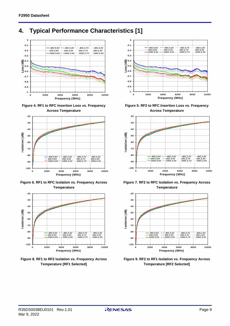
4. Typical Performance Characteristics [1]
Figure 4. RF1 to RFC Insertion Loss vs. Frequency
Across Temperature Figure 5. RF2 to RFC Insertion Loss vs. Frequency
Across Temperature
Figure 6. RF1 to RFC Isolation vs. Frequency Across
Temperature Figure 7. RF2 to RFC Isolation vs. Frequency Across
Temperature
Figure 8. RF1 to RF2 Isolation vs. Frequency Across Temperature [RF1 Selected]
Figure 9. RF2 to RF1 Isolation vs. Frequency Across Temperature [RF2 Selected]
-1
-0.9
-0.8
-0.7
-0.6
-0.5
-0.4
-0.3
-0.2
-0.1
0
0 2000 4000 6000 8000 10000
Loss
(dB)
Frequency (MHz)
-40C 5.5V -40C 3.3V -40C 2.7V -40C 2.3V25C 5.5V 25C 3.3V 25C 2.7V 25C 2.3V105C 5.5V 105C 3.3V 105C 2.7V 105C 2.3V
-1
-0.9
-0.8
-0.7
-0.6
-0.5
-0.4
-0.3
-0.2
-0.1
0
0 2000 4000 6000 8000 10000
Loss
(dB)
Frequency (MHz)
-40C 5.5V -40C 3.3V -40C 2.7V -40C 2.3V25C 5.5V 25C 3.3V 25C 2.7V 25C 2.3V105C 5.5V 105C 3.3V 105C 2.7V 105C 2.3V
-100
-90
-80
-70
-60
-50
-40
-30
-20
0 2000 4000 6000 8000 10000
Isol
atio
n (d
B)
Frequency (MHz)
-40C 5.5V -40C 3.3V -40C 2.7V -40C 2.3V25C 5.5V 25C 3.3V 25C 2.7V 25C 2.3V105C 5.5V 105C 3.3V 105C 2.7V 105C 2.3V
-100
-90
-80
-70
-60
-50
-40
-30
-20
0 2000 4000 6000 8000 10000
Isol
atio
n (d
B)
Frequency (MHz)
-40C 5.5V -40C 3.3V -40C 2.7V -40C 2.3V25C 5.5V 25C 3.3V 25C 2.7V 25C 2.3V105C 5.5V 105C 3.3V 105C 2.7V 105C 2.3V
-100
-90
-80
-70
-60
-50
-40
-30
-20
0 2000 4000 6000 8000 10000
Isol
atio
n (d
B)
Frequency (MHz)
-40C 5.5V -40C 3.3V -40C 2.7V -40C 2.3V25C 5.5V 25C 3.3V 25C 2.7V 25C 2.3V105C 5.5V 105C 3.3V 105C 2.7V 105C 2.3V
-100
-90
-80
-70
-60
-50
-40
-30
-20
0 2000 4000 6000 8000 10000
Isol
atio
n (d
B)
Frequency (MHz)
-40C 5.5V -40C 3.3V -40C 2.7V -40C 2.3V25C 5.5V 25C 3.3V 25C 2.7V 25C 2.3V105C 5.5V 105C 3.3V 105C 2.7V 105C 2.3V
F2950 Datasheet
R35DS0038EU0101 Rev.1.01 Mar 9, 2022
Page 10
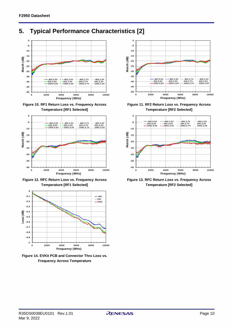
5. Typical Performance Characteristics [2]
Figure 10. RF1 Return Loss vs. Frequency Across
Temperature [RF1 Selected] Figure 11. RF2 Return Loss vs. Frequency Across
Temperature [RF2 Selected]
Figure 12. RFC Return Loss vs. Frequency Across
Temperature [RF1 Selected] Figure 13. RFC Return Loss vs. Frequency Across
Temperature [RF2 Selected]
Figure 14. EVKit PCB and Connector Thru Loss vs. Frequency Across Temperature
-50
-45
-40
-35
-30
-25
-20
-15
-10
-5
0
0 2000 4000 6000 8000 10000
Mat
ch (d
B)
Frequency (MHz)
-40C 5.5V -40C 3.3V -40C 2.7V -40C 2.3V25C 5.5V 25C 3.3V 25C 2.7V 25C 2.3V105C 5.5V 105C 3.3V 105C 2.7V 105C 2.3V
-50
-45
-40
-35
-30
-25
-20
-15
-10
-5
0
0 2000 4000 6000 8000 10000
Mat
ch (d
B)
Frequency (MHz)
-40C 5.5V -40C 3.3V -40C 2.7V -40C 2.3V25C 5.5V 25C 3.3V 25C 2.7V 25C 2.3V105C 5.5V 105C 3.3V 105C 2.7V 105C 2.3V
-40
-35
-30
-25
-20
-15
-10
-5
0
0 2000 4000 6000 8000 10000
Mat
ch (d
B)
Frequency (MHz)
-40C 5.5V -40C 3.3V -40C 2.7V -40C 2.3V25C 5.5V 25C 3.3V 25C 2.7V 25C 2.3V105C 5.5V 105C 3.3V 105C 2.7V 105C 2.3V
-40
-35
-30
-25
-20
-15
-10
-5
0
0 2000 4000 6000 8000 10000
Mat
ch (d
B)
Frequency (MHz)
-40C 5.5V -40C 3.3V -40C 2.7V -40C 2.3V25C 5.5V 25C 3.3V 25C 2.7V 25C 2.3V105C 5.5V 105C 3.3V 105C 2.7V 105C 2.3V
-1
-0.9
-0.8
-0.7
-0.6
-0.5
-0.4
-0.3
-0.2
-0.1
0
0 2000 4000 6000 8000 10000
Loss
(dB)
Frequency (MHz)
-40C25C105C
F2950 Datasheet
R35DS0038EU0101 Rev.1.01 Mar 9, 2022
Page 11
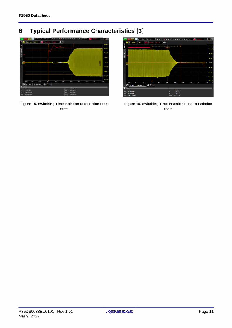
6. Typical Performance Characteristics [3]
Figure 15. Switching Time Isolation to Insertion Loss State
Figure 16. Switching Time Insertion Loss to Isolation State
F2950 Datasheet
R35DS0038EU0101 Rev.1.01 Mar 9, 2022
Page 12
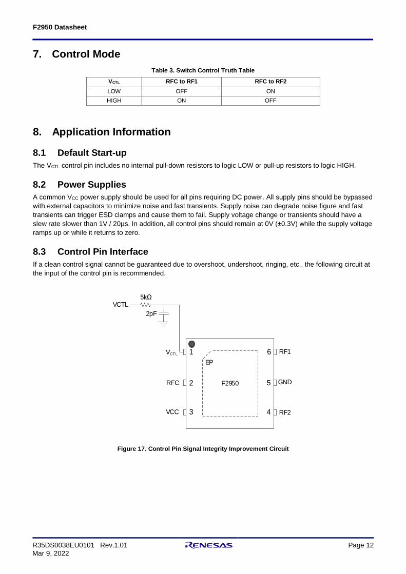
7. Control Mode Table 3. Switch Control Truth Table
VCTL RFC to RF1 RFC to RF2 LOW OFF ON HIGH ON OFF
8. Application Information
8.1 Default Start-up The VCTL control pin includes no internal pull-down resistors to logic LOW or pull-up resistors to logic HIGH.
8.2 Power Supplies A common VCC power supply should be used for all pins requiring DC power. All supply pins should be bypassed with external capacitors to minimize noise and fast transients. Supply noise can degrade noise figure and fast transients can trigger ESD clamps and cause them to fail. Supply voltage change or transients should have a slew rate slower than 1V / 20µs. In addition, all control pins should remain at 0V (±0.3V) while the supply voltage ramps up or while it returns to zero.
8.3 Control Pin Interface If a clean control signal cannot be guaranteed due to overshoot, undershoot, ringing, etc., the following circuit at the input of the control pin is recommended.
VCTL2pF
5kΩ
RF2
VCTL
GND
RF1
VCC
1
2
3
6
5
4
EP
RFC F2950
Figure 17. Control Pin Signal Integrity Improvement Circuit
F2950 Datasheet
R35DS0038EU0101 Rev.1.01 Mar 9, 2022
Page 13
9. Evaluation Kit
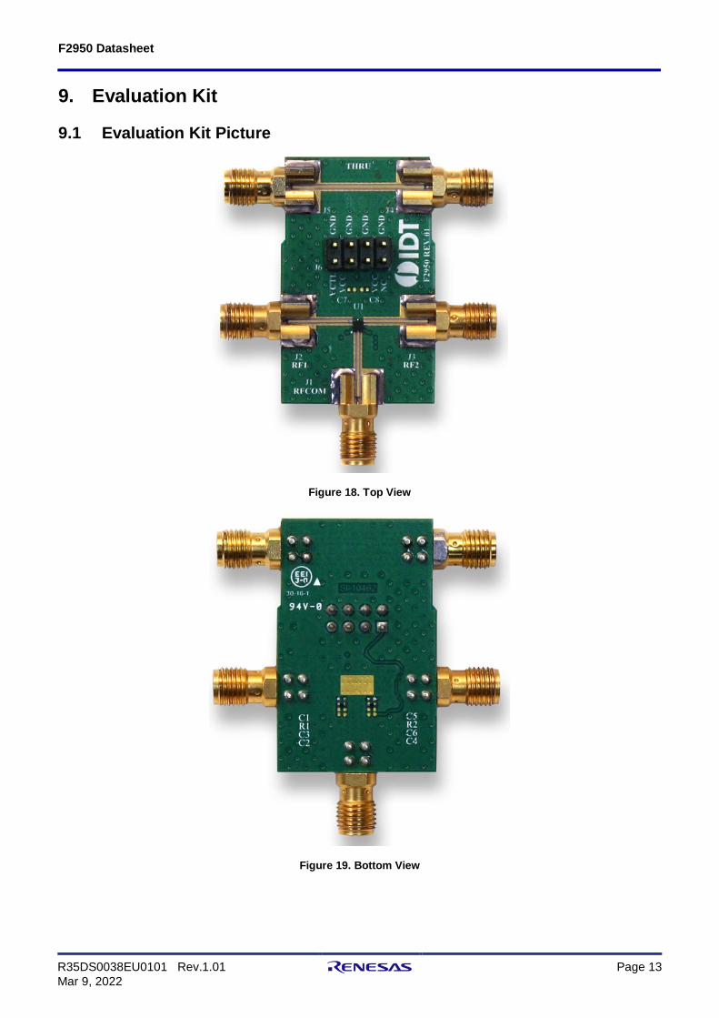
9.1 Evaluation Kit Picture
Figure 18. Top View
Figure 19. Bottom View
F2950 Datasheet
R35DS0038EU0101 Rev.1.01 Mar 9, 2022
Page 14
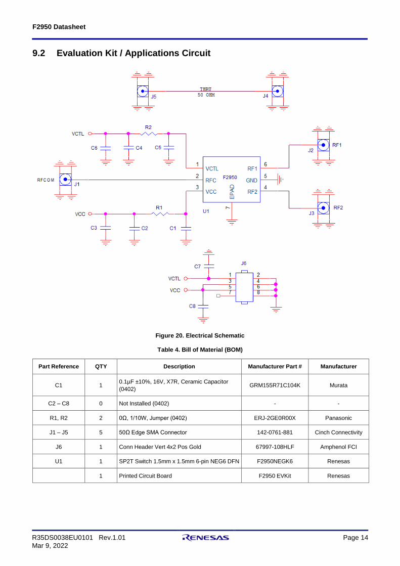
9.2 Evaluation Kit / Applications Circuit
Figure 20. Electrical Schematic
Table 4. Bill of Material (BOM)
Part Reference QTY Description Manufacturer Part # Manufacturer
C1 1 0.1µF ±10%, 16V, X7R, Ceramic Capacitor (0402) GRM155R71C104K Murata
C2 – C8 0 Not Installed (0402) - -
R1, R2 2 0Ω, 1/10W, Jumper (0402) ERJ-2GE0R00X Panasonic
J1 – J5 5 50Ω Edge SMA Connector 142-0761-881 Cinch Connectivity
J6 1 Conn Header Vert 4x2 Pos Gold 67997-108HLF Amphenol FCI
U1 1 SP2T Switch 1.5mm x 1.5mm 6-pin NEG6 DFN F2950NEGK6 Renesas
1 Printed Circuit Board F2950 EVKit Renesas
F2950 Datasheet
R35DS0038EU0101 Rev.1.01 Mar 9, 2022
Page 15
9.3 Evaluation Kit (EVKit) Operation 9.3.1. External Supply Setup 1. Set up a VCC power supply in the voltage range of 2.7V to 5.5V with the power supply output disabled. 2. Connect the disabled VCC supply connection to J6 pin 3 or 5 and GND to J6 pin 2, 4, 6, or 8.
9.3.2. Logic Control Setup 1. With the logic control line disabled, set the logic HIGH and LOW levels to satisfy the levels stated in the
electrical specifications table. 2. Connect the disabled logic control line to VCTL (pin 1 of J6) and GND to J6 pin 2, 4, 6, or 8.
9.3.3. Turn On Procedure 1. Set up the supplies and EVKit as noted in the External Supply Setup and Logic Control Setup sections
above. 2. Enable the VCC supply. 3. Enable the logic control signal. 4. Set the VCTL logic setting to achieve the desired Table 3 configuration. Note that the VCTL control logic
should not be applied without VCC being present. 5. Enable any RF signal.
9.3.4. Turn Off Procedure 1. Disable any applied RF signal. 2. Set VCTL to GND. 3. Disable the VCC supply.
F2950 Datasheet
R35DS0038EU0101 Rev.1.01 Mar 9, 2022
Page 16
10. Package Outline Drawings The package outline drawings are located at the end of this document and are accessible from the Renesas website. The package information is the most current data available and is subject to change without revision of this document.
11. Marking Diagram
YBA 2
Line 1: Y = last digit of the year, BA = sequential letters for traceability purposes Line 2: Pin 1 dot, 2 = F2950 part number code
12. Ordering Information
Part Number Package Description MSL Rating Carrier Type Temperature Range
F2950NEGK 1.5mm x 1.5mm x 0.55mm NEG6 DFN
MSL1 Cut Tape -40°C to +105°C
F2950NEGK8 MSL1 Reel
F2950EVBI Evaluation Board
13. Revision History
Revision Date Description
1.01 Mar 9, 2022 Updated the IIP2 specifications.
1.00 Aug 8, 2017 Initial release.
Corporate HeadquartersTOYOSU FORESIA, 3-2-24 Toyosu,Koto-ku, Tokyo 135-0061, Japanwww.renesas.com
Contact InformationFor further information on a product, technology, the most up-to-date version of a document, or your nearest sales office, please visit:www.renesas.com/contact/
TrademarksRenesas and the Renesas logo are trademarks of Renesas Electronics Corporation. All trademarks and registered trademarks are the property of their respective owners.
IMPORTANT NOTICE AND DISCLAIMER
RENESAS ELECTRONICS CORPORATION AND ITS SUBSIDIARIES (“RENESAS”) PROVIDES TECHNICAL SPECIFICATIONS AND RELIABILITY DATA (INCLUDING DATASHEETS), DESIGN RESOURCES (INCLUDING REFERENCE DESIGNS), APPLICATION OR OTHER DESIGN ADVICE, WEB TOOLS, SAFETY INFORMATION, AND OTHER RESOURCES “AS IS” AND WITH ALL FAULTS, AND DISCLAIMS ALL WARRANTIES, EXPRESS OR IMPLIED, INCLUDING, WITHOUT LIMITATION, ANY IMPLIED WARRANTIES OF MERCHANTABILITY, FITNESS FOR A PARTICULAR PURPOSE, OR NON-INFRINGEMENT OF THIRD PARTY INTELLECTUAL PROPERTY RIGHTS.
These resources are intended for developers skilled in the art designing with Renesas products. You are solely responsible for (1) selecting the appropriate products for your application, (2) designing, validating, and testing your application, and (3) ensuring your application meets applicable standards, and any other safety, security, or other requirements. These resources are subject to change without notice. Renesas grants you permission to use these resources only for development of an application that uses Renesas products. Other reproduction or use of these resources is strictly prohibited. No license is granted to any other Renesas intellectual property or to any third party intellectual property. Renesas disclaims responsibility for, and you will fully indemnify Renesas and its representatives against, any claims, damages, costs, losses, or liabilities arising out of your use of these resources. Renesas' products are provided only subject to Renesas' Terms and Conditions of Sale or other applicable terms agreed to in writing. No use of any Renesas resources expands or otherwise alters any applicable warranties or warranty disclaimers for these products.
(Rev.1.0 Mar 2020)
© 2020 Renesas Electronics Corporation. All rights reserved.