ED
36
Chapter I Electronic Materials and Device Electronic Materials and Device Electronic Materials and Device Electronic Materials and Device Electronic Materials and Devices 1. The forbidden charge in germanium at 0°K is (a) 0.785 eV (b) 1.21 eV (c) 1.00 eV (d) 0.01 eV 2. One electron volt equals to (a) 01.60 × 10 –19 (b) 09.11 × 10 –31 (c) 19.40 × 10 –10 (d) 01.16 × 10 –19 3. Which device is a combination of P-N junction diode and two resistors? (a) SCR (b) SCS (c) UJT (d) FET 4. The α of the transistor is (a) A measure of its sensitivity (b) A measure of quality (c) A measure of thermal stability (d) A measure of its noise immunity 5. Which of the following is also known as reverse blocking triode thyristor? (a) Triac (b) Diac (c) SCR (d) UJT 6. In germanium the majority of electrons are (a) 1.22 m 2 /Vs (b) 1.44 m 2 /Vs (c) 1.66 m 2 /Vs (d) 1.88 m 2 /Vs 7. While plotting the V-I characteristics of semi- conductor diode, the voltage is plotted along horizontal axis and the current along the vertical axis because (a) The voltage and currents are independent variables (b) The voltage and currents are dependent variables (c) The voltage is dependent and the current is independent variable (d) The voltage and the current are dependent variables 8. In order to increase the recombination rate in silicon PN junction device _________ is diffused. (a) Aluminum (b) Silver (c) Indium (d) Gold 9. One electron volt equals to (a) 1.620 × 10 –19 (b) 1.602 × 10 –19 (c) 1.620 × 10 –18 (d) 1.602 × 10 –18 10. During IC fabrication, the chemical reaction involved in epitaxial growth takes place at a temperature of about (a) 500 °C (b) 1000 °C (c) 1200 °C (d) 1500 °C 11. If the PN junction is abrupt, the capacitance varies as (a) Square root of reverse bias (b) Square of reverse bias (c) Cube root of reverse bias (d) Cube of reverse bias 12. Match list I and list II and select the correct one using the codes given below: List I List II P. Resistance 1. Current noise Q. Diode 2. Partition noise R. Triode 3. Shot noise S. PN junction 4. Johnson noise
-
Upload
saideep-narasimhan -
Category
Documents
-
view
29 -
download
2
Transcript of ED
Chapter I
Electronic Materials and DeviceElectronic Materials and DeviceElectronic Materials and DeviceElectronic Materials and DeviceElectronic Materials and Devicesssss
1. The forbidden charge in germanium at 0°K is(a) 0.785 eV (b) 1.21 eV(c) 1.00 eV (d) 0.01 eV
2. One electron volt equals to(a) 01.60 × 10⁻¹⁹ (b) 09.11 × 10⁻³¹
(c) 19.40 × 10⁻¹⁰ (d) 01.16 × 10⁻¹⁹
3. Which device is a combination of P-N junctiondiode and two resistors?(a) SCR (b) SCS(c) UJT (d) FET
4. The ααααα of the transistor is(a) A measure of its sensitivity(b) A measure of quality(c) A measure of thermal stability(d) A measure of its noise immunity
5. Which of the following is also known as reverseblocking triode thyristor?(a) Triac (b) Diac(c) SCR (d) UJT
6. In germanium the majority of electrons are(a) 1.22 m2/Vs (b) 1.44 m2/Vs(c) 1.66 m2/Vs (d) 1.88 m2/Vs
7. While plotting the V-I characteristics of semi-conductor diode, the voltage is plotted alonghorizontal axis and the current along the verticalaxis because(a) The voltage and currents are independent
variables(b) The voltage and currents are dependent
variables
(c) The voltage is dependent and the current isindependent variable
(d) The voltage and the current are dependentvariables
8. In order to increase the recombination rate in siliconPN junction device _________ is diffused.(a) Aluminum (b) Silver(c) Indium (d) Gold
9. One electron volt equals to(a) 1.620 × 10⁻¹⁹
(b) 1.602 × 10⁻¹⁹
(c) 1.620 × 10⁻¹⁸
(d) 1.602 × 10⁻¹⁸
10. During IC fabrication, the chemical reactioninvolved in epitaxial growth takes place at atemperature of about(a) 500 °C (b) 1000 °C(c) 1200 °C (d) 1500 °C
11. If the PN junction is abrupt, the capacitance variesas(a) Square root of reverse bias(b) Square of reverse bias(c) Cube root of reverse bias(d) Cube of reverse bias
12. Match list I and list II and select the correct oneusing the codes given below:
List I List IIP. Resistance 1. Current noiseQ. Diode 2. Partition noiseR. Triode 3. Shot noiseS. PN junction 4. Johnson noise
2 Question Bank on Electronics Technology
(a) P- (4), Q - (1), R- (2), S- (3)(b) P- (2), Q - (3), R- (1), S- (4)(c) P- (1), Q - (2), R- (3), S- (4)(d) P- (4), Q - (3), R- (2), S- (1)
13. In a semiconductor diode, the time constant equalsto(a) Value of majority carrier lifetime(b) Value of minority carrier lifetime(c) Diffusion capacitance time constant(d) Zero
14. A Triac has(a) 2 layers (b) 3 layers(c) 4 layers (d) 5 layers
15. Thyristors can be used to perform(a) Rectification (b) Inversion(c) Regulation (d) All of the above
16. Normal biasing of transistor is(a) Forward bias the Emitter-Base and reverse bias
the Collector-Base(b) Forward bias both the Emitter-Base and
Collector-Base(c) Reverse bias both the Emitter-Base and
Collector-Base(d) Reverse bias both Emitter-Base and forward
bias the Collector-Base
17. With reference to the current amplification factorof transistor(a) α is greater than β(b) α is smaller than β(c) α and β are equal(d) None of the above
18. For small values of drain to source voltage, JFETbehaves like a(a) Diode (b) Capacitor(c) Inverter (d) Resistor
19. A thyristor is fabricated using(a) Silicon(b) Germanium(c) Gallium arsenide(d) Indium oxide
20. An SCR is a semiconductor device, which consistsof(a) 4 PN junctions(b) 3 PN junctions(c) 2 PN junctions(d) 1 PN junction
21. Input impedance of MOSFET is(a) Less than BJT but more than FET(b) More than BJT but less than FET(c) More than BJT and FET(d) Less than BJT and FET
22. When a transistor is connected in common collectormode, then(a) Input is in between Base and Emitter(b) Input is in between Base and Collector(c) Input is in between Emitter and Collector(d) Input is in between Collector short-circuited
23. In general, a shell contains a maximum of________ electrons.(a) 2n (b) 2n2
(c) 2n–1 (d) 2n+1
24. The holding current IH of the SCR is(a) Inversely proportional to the temperature(b) Directly proportional to the temperature(c) Remains unaffected by variation in
temperature(d) None of the above
25. Which one of the following possesses negativeresistance characteristics?(a) Schottky diode(b) Tunnel diode(c) PN junction diode(d) Hot-carrier diode
26. As the temperature increases in a semiconductor,the densities of the electrons and holes(a) Increase (b) Decrease(c) Become equal (d) Can’t be defined
27. A glass is a/an(a) Good conductor(b) Semiconductor(c) Insulator(d) Resistive material
28. An ideal diode can be considered as an(a) Amplifier (b) Bi-stable switch(c) Oscillator (d) Fuse
29. Emission of a beta particle from an atom(a) Increases the number of protons in an atom(b) Increases the number of neutrons in an atom(c) Decreases the number of protons in an atom(d) Decreases the number of neutrons in an atom
Electronic Materials and Devices 3
30. A voltage regulator is based on the principle of(a) Rectification(b) Amplification(c) Zener breakdown(d) Avalanche breakdown
31. Which of the following doesn’t have forbiddenenergy gap between valence band and conductorband?(a) Conductor(b) Insulator(c) Semiconductor(d) None of the above
32. An SCR is(a) 3 layer, tri-junction device(b) 3 layer, four-junction device(c) 4 layer, tri-junction device(d) 4 layer, four-junction device
33. An LED is made up of(a) Phosphorescent material(b) Germanium(c) Silicon(d) Gallium arsenide
34. The conductivity of the intrinsic semiconductor atabsolute temperature is(a) 1.1 eV (b) 0.63 eV(c) Zero (d) Infinity
35. The region between the peak and valley points ofthe tunnel diode is called as(a) Pinch-off region(b) Saturation region(c) Cut-off region(d) Negative conduction region
36. Avalanche breakdown occurs when(a) The forward current is excessive(b) The forward bias exceeds a certain value(c) The reverse bias exceeds a certain value(d) The potential barrier is reduced to zero
37. Doping is a process of(a) Purifying semiconductor material(b) Increasing impurity percentage(c) Removal of foreign atoms(d) Increasing the bias potential
38. With reference to transistor which of the followingis correct?(a) IC = IE + IB(b) IB = IC + IE(c) IE = IB + IC(d) IE = IB
39. A Silicon-controlled switch is(a) A unilateral device without a gate(b) A unilateral device with 2 gates(c) A bilateral device without a gate(d) A bilateral device with 2 gates
40. The intrinsic stand-off ratio of UJT is(a) Always equal to zero(b) Always equal to unity(c) Always greater than unity(d) Always less than unity
41. Zener diode exhibits(a) Avalanche breakdown(b) Zener breakdown(c) Both (a) & (b)(d) Neither (a) nor (b)
42. In a transistor, if the base current is 1 mA andcollector current is 2 mA, then(a) IE = 1 mA(b) IE = 2 mA(c) IE = 3 mA(d) IE = 4 mA
43. A BJT has(a) One PN junction(b) Two PN junctions(c) Three PN junctions(d) Four PN junctions
44. The switching time of LED is in the order of(a) 1 second(b) 1 microsecond(c) 1 millisecond(d) 1 nanosecond
45. For a doped semiconductor material, the dynamicresistance is(a) Small and can be neglected(b) Large and can be neglected(c) Small but cannot be neglected(d) Large but cannot be neglected
46. __________ is an example of acceptor material.(a) Gallium (b) Arsenide(d) Bismuth (d) Antimony
47. The βββββ value of a transistor can be determined fromthe curve plotted between(a) VB E and IE for constant VC E
(b) VB E and IC for constant VC E
(c) VC E and IE for constant IB
(d) VC E and IC for constant IB
4 Question Bank on Electronics Technology
48. When a semiconductor is heavily doped in a rangeof 1017 to 1018 impurity atoms/cm3, then it behavesas(a) Intrinsic semiconductor(b) Extrinsic semiconductor(c) Simply as semiconductor(d) Degenerative semiconductor
49. The DC current gain of a transistor is(a) Always positive and greater than unity(b) Always positive and less than unity(c) Always positive and equal to unity(d) Always positive and equal to infinity
50. The Collector to Base with Emitter open current, atransistor is extremely temperature dependentbecause(a) It is made up of free electrons and holes(b) It is made up of thermally generated majority
carrier(c) It is made up of thermally generated minority
carrier(d) It is made up of free electrons alone
51. Diac can be analyzed by imaging it as(a) Two diodes connected in series(b) Two diodes connected in parallel(c) Two diodes connected in anti-parallel
connection(d) One transistor and a diode connected
parallelly
52. Graphite is a(a) Conductor(b) Insulator(c) Semiconductor(d) None of these
53. Tunnel diode, with its negative resistancecharacteristics can be employed for(a) Current amplification(b) Voltage amplification(c) Power amplification(d) All of the above
54. Thermistor is a device whose resistance(a) Decreases proportionally with increase in
temperature(b) Decreases exponentially with increase in
temperature(c) Increases proportionally with increase in
temperature(d) Increases exponentially with increase in
temperature
55. Capacitive effects are exhibited by PN junctionswhen they are(a) Forward biased(b) Reverse biased(c) Either forward or reverse biased(d) Neither forward nor reverse biased
56. Which of the following elements is the poorest con-ductor of heat?(a) Sodium (b) Lead(c) Zinc (d) Mercury
57. What is the type of capacitance effect exhibitedby the PN junction, when it is reverse biased?(a) Transition capacitance(b) Diffusion capacitance(c) Space charge capacitance(d) Drift capacitance
58. Localized hot spots and device destruction cantake place in power transistors due to(a) Avalanche breakdown(b) Primary breakdown(c) Second breakdown(d) Quasi-saturation breakdown
59. Recombination of electrons and holes takes placewhen(a) An electron falls into a hole(b) A positive ion and a negative ion bond together(c) Avalanche electron becomes a conduction elec-
tron(d) An atom is formed
60. The power consumption of an LCD as comparedto an LED is(a) Same (b) More(c) Less (d) Can’t be defined
61. When a photodiode is reverse biased, and kept ina dark room, the current flowing through the devicecorresponds to(a) Zero current(b) Maximum current the device can hold(c) Normal current that flows through the device(d) Reverse saturation current
62. If an atom has an atomic number of 6, then it has(a) 3 electrons & 3 protons(b) 4 electrons & 2 protons(c) 2 electrons & 4 protons(d) 6 electrons & 6 protons
Electronic Materials and Devices 5
63. Semiconductors are(I) Ohmic as they obey Ohm’s law(II) Bipolar(a) Only I is true(b) Only II is true(c) Both I & II are true(d) Both I & II are false
64. An SCR can be constructed using(a) One PNP and one NPN transistor(b) Two PNP transistors(c) Two NPN transistors(d) All of the above
65. The current amplification factor of ααααα of a transis-tor is always(a) Less than 1 (b) Greater than 1(c) Equal to 1 (d) None of these
66. Match the followingP. SCR (I) Low current SCR
without gateQ. Triac (II) Low current SCR
with gateR. Schottky diode (III) Uni-directionalS. SCS (IV) Bi-directional
(a) P-IV, Q-III, R-I, S-II(b) P-I, Q-II, R-III, S-IV(c) P-III, Q-IV, R-I, S-II(d) P-I, Q-IV, R-II, S-III
67. Silicon is appreciably employed as a base materialcompared to germanium while manufacturingZener diode since(a) Silicon is abundantly available(b) It is costlier(c) It has low current capability(d) It has high temperature capability
68. The input impedance of FET(a) Is less than 10 kΩ(b) Is greater than 10 MΩ(c) Falls within a range between 10 kΩ and 10
MΩ(d) Is less than 1 kΩ
69. An excited electron in an atom returns to the groundstate(a) Always in one jump(b) In one or more jumps(c) Always in two jumps(d) Always in three jumps
70. Which one of the following pair is correctlymatched?
(a) Mass spectroscopy - Chadwick(b) Atomic number - Moseley(c) Neutron - Millikan(d) Measurement of
charge of an electron - Aston
71. Impact ionization is a process of liberation of freeelectrons by breaking(a) Metallic bond(b) Ionic bond(c) Covalent bond(d) van der Waals bond
72. A forward biased diode(a) Acts as an open switch(b) Offers high resistance(c) Has a large voltage drop(d) Conducts current easily
73. UJT can be used as(a) Oscillator(b) Amplifier(c) Oscillator and amplifier(d) Either as oscillator or amplifier
74. In a Zener diode(a) P & N regions are lightly doped(b) The depletion region is wide(c) P & N regions are heavily doped(d) The junction field current is small
75. Which of the following statements are correct?1. In semiconductor, the mobility of electrons is
more than that of holes2. In semiconductor, when temperature increases,
the resistivity also increases3. Metal has positive TCR4. In metals, thermal conductivity is inversely
proportional to electrical conductivity atconstant temperature
(a) 1, 2, 3 (b) 1, 2, 4(c) 2, 3, 4 (d) 1, 3, 4
76. The atomic number of silicon is(a) 14 (b) 16(c) 18 (d) 12
77. The common method of making PN junction isknown as(a) Diffusing(b) Alloying(c) Doping(d) Biasing
6 Question Bank on Electronics Technology
78. As compared to PNP transistor, NPN transistorsare preferred due to(a) Economical(b) Simple operating mechanism(c) Consumes less bias voltage(d) Better high frequency response
79. In tunnel diode, the impurity concentration is inthe order of(a) 1 part in 1010 parts(b) 1 part in 106 parts(c) 1 part in 109 parts(d) 1 part in 103 parts
80. The transport factor of common emitter circuit isgiven as(a) ΔIC/ΔIE
(b) ΔIC/ΔIB
(c) ΔIE/ΔIB
(d) ΔIC= ΔIE + ΔIB
81. The dynamic resistance of diode is(a) Constant and independent of operating voltage(b) Constant and dependent on operating voltage(c) Not a constant and independent of operating
voltage(d) Not a constant and dependent on operating
voltage
82. The carrier mobility in a semiconductor is foundto be 0.4 m2/VS. Its diffusion constant at 300 K willbe(a) 0.43 m2/s (b) 0.16 m2/s(c) 0.04 m2/s (d) 0.01 m2/s
83. Which diode is otherwise known as ESAKI diode?(a) PIN diode(b) Schottky barrier diode(c) GUNN diode(d) Tunnel diode
84. The Hall coefficient of an intrinsic semiconductoris(a) Positive under all conditions(b) Negative under all conditions(c) Zero under all conditions(d) Zero at 0°K
85. Two elements that are frequently used for makingtransistors are(a) Iridium and Tungsten(b) Lead and Tin
(c) Iron and Carbon(d) Silicon and Germanium
86. IGBT combines the(a) Switching characteristics of JFET with power
handling capacity of BJT(b) Switching characteristics of MOSFET with
power handling capacity of BJT(c) Switching characteristics of BJT with power
handling capacity of JFET(d) Switching characteristics of BJT with power
handling capacity of MOSFET
87. The best conductor of heat among the liquids is(a) Water (b) Mercury(c) Ether (d) Alcohol
88. Consider the following statements regarding asemiconductor1. Acceptor level lies close to valence band2. Donor level lies close to valence band3. N-type semiconductor behaves as a conductor
at 0°K4. P-type semiconductor behaves as an insulator
at 0°K(a) 1 & 2 are correct (b) 1 & 3 are correct(c) 1 & 4 are correct (d) 2 & 3 are correct
89. The current in a PMOS transistor is(a) Less than thrice that in an NMOS device(b) Greater than thrice that in a PMOS device(c) Less than half of that in an NMOS device(d) Greater than half of that in a WMOS device
90. In a semiconductor, the total current is equal to
(a) Sum of electron and hole currents flow in samedirection
(b) Sum of electron and hole currents flow inopposite directions
(c) Electron current only(d) Hole current only
91. Semiconductor materials are made up of(a) Metallic bond(b) Ionic bond(c) Un-shared bond(d) Covalent bond
92. The barrier potential of Schottky diode is(a) 0.25 V (b) 0.35 V(c) 0.45 V (d) 0.56 V
Electronic Materials and Devices 7
93. Consider the statements with respect to semi-conductor breakdown.
Statement 1: The Zener breakdown occurs injunctions which are lightly doped.
Statement 2: The avalanche breakdown occurs injunctions, which are heavily doped.(a) Statements 1 & 2 are correct(b) Only statement 1 is correct(c) Only statement 2 is correct(d) Statements 1 & 2 are wrong
94. In a PN junction, the density of carriers is _______near the junction and decays _______ withdistance.(a) Low, linearly(b) High, linearly(c) Low, exponentially(d) High, exponentially
95. Which type of the following structures containstwo atoms per cell?(a) Body centered cubic(b) Face centered cubic(c) Single cubic cell(d) None of the above
96. The turn-on time of a typical transistor is equalto(a) Delay time(b) Rise time(c) Storage time(d) Sum of delay time & rise time
97. Consider the following statements:1. The bulk resistance is observed when diode is
reverse biased2. The junction resistance of a diode is variable
resistance(a) 1 is correct(b) 1 & 2 are correct(c) 2 is correct(d) 1 is wrong but 2 is correct
98. A particle of zero initial velocity placed inside auniform magnetic field will(a) Move in zigzag directions along the line of flux(b) Move with varying speed(c) Move with constant speed along the line of force(d) Move with constant speed opposite to the line
of force
99. Across a varactor diode, an increase in its reversebias potential causes
(a) Width of depletion layer to increase thusincreasing the capacitance
(b) Width of depletion layer to decrease thusincreasing the capacitance
(c) Width of depletion layer to increase thusdecreasing the capacitance
(d) Width of depletion layer to decrease thusdecreasing the capacitance
100. The germanium diode at room temperature for aforward current of 26 mA has dynamic resistanceof about(a) 100 Ω (b) 10 Ω(c) 1 Ω (d) 0.1 Ω
101. Silicon can appreciably be employed as basematerial as compared to germanium whilemanufacturing Zener diode because(a) Silicon is abundantly available(b) It is not costlier(c) Low current capability(d) High temperature capacity
102. The maximum number of electron that an M-shellof an atom can contain is(a) 4 (b) 12(c) 18 (d) 34
103. As the temperature is increased, the voltage acrossthe diode carrying constant current(a) Increases(b) Decreases(c) Remains constant(d) Fluctuates between low and high threshold
values
104. Current flow in the semiconductor slap is due to(a) Drift phenomenon(b) Diffusion phenomenon(c) Recombination phenomenon(d) All of the above
105. If CT = space change capacitance and CD= storagecapacitance of PN junction diode, then(a) CT = CD (b) CT > CD
(c) CT < CD (d) CT = CD = ∞
106. At low temperature, the resistivity of metals isproportional to the(a) 5th power of absolute temperature(b) 6th power of absolute temperature(c) 7th power of absolute temperature(d) 9th power of absolute temperature
8 Question Bank on Electronics Technology
107. Which one is the valid statement with respect toPN junction diode?(a) Under forward bias, the electrons from P
region & holes from N region drift towardsthe junction
(b) A junction diode cannot be used as a switch inelectrical circuits
(c) Depletion capacitance is voltage independent(d) Diffusion current of minority carriers is
proportional to the concentration gradient
108. In intrinsic semiconductor(a) The electron density is twice the hole density(b) The electron density is thrice the hole density(c) The electron density is square root of the hole
density(d) The electron density is same as the hole density
110. The Fermi-Dirac probability function specifyingall states at energy E (electron volts) occupiedunder the thermal equilibrium is given by(a) f(E) = KT – ln eE-Ef
(b) f(E) = 1 + eE-Ef
(c) f(E) = 1( 1 + e(E-Ef) / kT)(d) f(E) = ((E)/Ef)e
-KT
111. Which among the following diodes has zerobreakdown voltage?(a) Zener diode(b) Schottky diode(c) Backward diode(d) Tunnel diode
112. Match list 1 with list 2 with respect to transistorbiasing
Biasing Region of operation(A) When EB & CB (1) Inverted
junctions areforward biased
(B) When EB & CB (2) Cut-offjunctions arereverse biased
(C) When EB is (3) Activeforward biased &CB is reverse biased
(D) When EB is reverse (4) Saturation& CB is forward biased
(a) A-1, B-2, C-3, D-4(b) A-4, B-2, C-3, D-1(c) A-4, B-3, C-2, D-1(d) A-4, B-1, C-3, D-2
113. A Zener diode may be thought as open for(a) 0V < V < VZ (b) 0V > V > VZ
(c) 0V > V < VZ (d) 0V < V > VZ
114. In silicon material, the mobility of free electron is(a) 2.5 m2/Vs (b) 2.7 m2/Vs(c) 1.66 m2/Vs (d) 2.33 m2/Vs
115. The dynamic resistance r of a diode varies as(a) 1/I (b) 1/I2
(c) I (d) I2
116. The reverse saturation current in germaniumdiode is of the order of(a) 1 nano amps(b) 1 micro amps(c) 1 milli amps(d) 1 kilo amps
117. The covalent crystals are characterized by(a) Good electrical conductivity and low hardness(b) Good electrical conductivity and high hardness(c) Poor electrical conductivity and high hardness(d) Poor electrical conductivity and low hardness
118. The diode capacitance has ______ temperaturecoefficient and the figure of merit has ______temperature coefficient.(a) Positive, Positive(b) Negative, Negative(c) Positive, Negative(d) Negative, Positive
119. A Schottky diode has
(a) Insulator - Semiconductor junction(b) Semiconductor - Semiconductor junction(c) Metal - Semiconductor junction(d) Metal - Metal junction
120. Which is the largest transistor current?
(a) Emitter current(b) Base current(c) Collector current(d) Both Emitter & Collector currents
121. A laser diode(a) Produces always light of single wavelength(b) Produces always light of multiple wavelength(c) Can be made to produce light of single and
multiple wavelengths(d) Produces visible light spectrum
Electronic Materials and Devices 9
122. Which type contains two atoms per cell?(a) Body centered cubic(b) Face centered cubic(c) Single cubic cell(d) None of the above
123. With reference to JFET configuration, match thefollowing
(P) Common Source (1) No phase shiftConfiguration between input &
output(Q) Common Drain (2) High input imped-
Configuration ance & low output
impedance(R) Common Gate (3) Source follower
Configuration
(a) P-1, Q-2, R-3(b) P-2, Q-3, R-1(c) P-2, Q-1, R-3(d) P-3, Q-1, R-2
124. A Nixie cold cathode glow discharge tube has(a) 20 cathodes (b) 15 cathodes(c) 14 cathodes (d) 10 cathodes
125. Consider the following statements1. LED is also known as direct gap diode2. LCD generates lightOf these statements(a) 1 is correct but 2 is wrong(b) 2 is correct but 1 is wrong(c) Both 1 & 2 are correct(d) Both 1 & 2 are wrong
126. The isolation capacitance of an opto coupler is inthe order of(a) 0.3 – 2.5 μF(b) 0.3 – 2.5 F(c) 0.3 – 2.5 pF(d) 0.3 – 2.5 nF
127. The light activated SCRs are sensitive to(a) Light(b) Temperature(c) Rate of change of applied voltage(d) All of the above
128. The light emitting diode(a) Usually made from metal oxide(b) Is Used in reverse biased condition(c) Gives light when temperature increases(d) Gives light due to electron hole recombination
129. The numeric aperture is the fiber optic cable’sability(a) To collect the light(b) To diffract the light(c) To reflect the light(d) To refract the light
130. The color emitted by an LED depends mainly on(a) Type of material used(b) Type of biasing applied(c) Recombination rate of charge carriers(d) Environmental conditions
131. The minority holes are about ______ that ofelectron.(a) Half (b) Same(c) Twice (d) Thrice
132. Compared to visible red light emitting diode, aninfrared LED(a) Produces light with longer wavelength(b) Produces light with shorter wavelength(c) Produces light with medium wavelength(d) Produces light of all wavelengths
133. At absolute zero temperature, an intrinsic semi-conductor behaves like a(a) Conductor(b) Insulator(c) Semiconductor(d) Other metals
134. Germanium and silicon are(a) Trivalent (b) Tetravalent(c) Pentavalent (d) Covalent
135. In comparison to LED, LASER has1. High emission frequency2. No tuning arrangement3. Narrow spectral bandwidth4. Provision for confinementOf these statements(a) 1, 3, & 4 are correct(b) 1, 2, & 3 are correct(c) 1 & 3 are correct(d) 2, 3, & 4 are correct
136. The volume charge density of mobile carriers isexpressed in(a) Coulombs / cubic meters(b) Coulombs / meters(c) Coulombs / seconds(d) Coulombs / volts
10 Question Bank on Electronics Technology
137. An LCD requires a power of about(a) 20 W (b) 20 mW(c) 20 μW (d) 20 nW
138. Barrier potential of PN junction decreases astemperature(a) Increases(b) Decreases(c) Remains constant(d) Increases & then decreases
139. Valence electrons are(a) In the closest orbit of the nucleus(b) In the most distant orbit from the nucleus(c) In the various orbits around the nucleus(d) Not associated with a particular atom
140. In a PIN diode, the intrinsic layer sandwichedbetween the heavily doped P & N layers is(a) Heavily doped(b) Lightly doped(c) Very lightly doped(d) Moderately doped
141. If an atom has an atomic number of 6, then it has(a) 3 electrons & 3 protons(b) 4 electrons & 2 protons(c) 2 electrons & 4 protons(d) 6 electrons & 6 protons
142. Transistor is said to be in a quiescent state when(a) It is unbiased(b) No current flows through it(c) No signal is applied to its input(d) Emitter junction is reverse biased
143. In a Silicon crystal, the number of covalent bondsa single atom can form is(a) 2 (b) 4(c) 6 (d) 8
144. Peak inverse voltage of the diode is found to be(a) Greater or equal to VM
(b) Small or equal to VM
(c) Equal to VM
(d) Not equal to VM
145. What is the type of capacitance effect exhibitedby the PN junction when it is forward biased?(a) Diffusion capacitance(b) Storage capacitance(c) Drift capacitance(d) Transition capacitance
146. Which of the following elements is most abundantin the earth’s crust?(a) Oxygen (b) Sulphur(c) Silicon (d) Carbon
147. A semiconductor has a resistivity which(a) Is smaller than 10-2 Ω-cm(b) Is larger than 10-2 Ω-cm(c) Varies between 10-2 Ω-cm and 10-9 Ω-cm(d) None of the above
148. In Bohr’s theory of atom, all the orbits of theelectrons are considered circular in shape. The deBroglie wavelength λλλλλn corresponding to theelectron in the nth orbit is(a) Proportional to n(b) Proportional to n2
(c) Inversely proportional to n(d) Inversely proportional to n2
149. The variable capacitance property possessed bythe reverse biased PN junction is used to constructa device known as(a) Zener diode (b) Volta caps(c) Gunn diode (d) Tunnel diode
150. Consider the following statements regarding Bohratomic model.
(Pick the right one)1. It introduces the idea of stationary orbit2. It assumes that angular momentum of electron
is equal to ½(h/2π)3. It uses planetary model of atom revolving in
circular orbit(a) 1 & 2 (b) 2 & 3(c) 1 & 3 (d) 1, 2 & 3
151. When an electron moves from a higher orbit to alower orbit(a) Emission of energy takes place(b) Absorption of energy takes place(c) Size of the atom increases(d) Either absorption or emission of energy takes
place
152. Emission of light in an LED results due to(a) Emission of electrons(b) Photovoltaic effect(c) Generation of electromagnetic radiation(d) Conversion of heat to electrical energy
153. Match the items in Group I with items in Group IImost suitably
Electronic Materials and Devices 11
Group I Group II(P) LED (1) Heavily doped(Q) Avalanche photo diode (2) Coherent radiation(R) Tunnel diode (3) Spontaneous emis-
sion(S) LASER (4) Current gain(a) P-2, Q-1, R-3, S-4(b) P-4, Q-3, R-2, S-1(c) P-3, Q-4, R-1, S-2(d) P-3, Q-2, R-1, S-4
154. Which of the following statements is/are correct?(a) Two discrete diodes connected back-to-back
can work as a transistor(b) Heat sink is a sheet of insulator used to
dissipate the heat developed at the collectorjunction of a power transistor
(c) The collector leakage current is stronglyindependent of temperature
(d) The collector junction of transistor is heavilydoped
155. Consider the following statements
Rutherford’s alpha particle scattering experimentproved that the nucleus1. Contains massive particles2. Is a +ve charge center3. Is quite stableWhich of the statements are correct?(a) 1, 2, 3 (b) 1, 2(c) 2, 3 (d) 1, 3
156. The Common-emitter amplifier is preferred toCommon-base amplifier due to(a) Higher amplification factor(b) Easy biasing network(c) Good stability(d) Economicity
157. When an electron moves from lower orbit to ahigher orbit(a) Emission of energy takes place(b) Absorption of energy takes place(c) Size of atom increases(d) Either absorption or emission of energy takes
place
158. Consider the statements1. Ideal diode conducts with zero resistance when
forward biased2. Ideal diode appears as an infinite resistance
when reverse biased(a) Only 1 is correct
(b) Only 2 is correct(c) Both 1 & 2 are correct(d) Either 1 or 2 is correct
159. The forbidden energy gap EG in a semiconductoris a function of(a) Current (b) Voltage(c) Potential (d) Temperature
160. Based on Quantum mechanical theory, the massof holes are ______ than the electrons.(a) Larger (b) Smaller(c) Equal (d) None of the above
161. The atomic number of germanium is(a) 24 (b) 26(c) 28 (d) 32
162. Dislocations are(a) Line defects(b) Planar defects(c) Point defects(d) Chemical defects
163. Intrinsic concentration of charge carriers in asemiconductor varies as(a) T (b) T2
(c) T3 (d) 1/T
164. On increasing the impurity concentration in themetal, the residual part of the resistivity(a) Decreases(b) Increases(c) Remains constant(d) May increase or decrease
165. At room temperature in intrinsic germanium, thereis about(a) One free electron for every 109 atoms(b) One free electron for every 1010 atoms(c) One free electron for every 1012 atoms(d) One free electron for every 1015 atoms
166. The UJT is a(a) Voltage controlled device(b) Current controlled device(c) Relaxation oscillator(d) None of these
167. The electrical conductivity is directly propor-tional to
(I) Electron density
(II) Relaxation time of electrons(a) Both I & II (b) Only II(c) Only I (d) Neither I nor II
12 Question Bank on Electronics Technology
168. A compensated semiconductor is doped with(a) Only donor impurities(b) Only acceptor impurities(c) Both donor and acceptor impurities(d) Neither donor nor acceptor impurity
169. Hall effect multiplier gives an output proportionalto the product of ______ signal.(a) Two (b) Three(c) Four (d) Infinite
170. The dynamic impedance of Zener diode _______with increase in the current flow through it.(a) Increases(b) Decreases(c) Remains unaffected(d) Is independent
171. Donor impurity atoms in a semiconductor resultsin the formation of new(a) Wide energy band(b) Narrow energy band(c) Discrete energy level just below conduction(d) Discrete energy level just above conduction
172. The depletion region of a semiconductor has(a) Only free electrons(b) Only holes(c) Both free electrons and holes(d) Absence of free electrons and holes
174. The electron density in conduction band isproportional to(a) Donor concentration(b) Square of donor concentration(c) Square root of donor concentration(d) Cube root of donor concentration
175. Capacitance is(a) Exponentially proportional to the time
constant(b) Linearly proportional to the time constant(c) Differentially proportional to the time constant(d) None of these
176. Diffusion capacitance is a capacitance of a(a) Reverse biased semiconductor diode junction
caused by unequal doping(b) Reverse biased semiconductor diode junction
caused by equal doping(c) Forward biased semiconductor diode junction
caused by unequal doping(d) Forward biased semiconductor diode junction
caused by equal doping
177. Constantan is a Copper-Nickel alloy consisting of(a) 60 % Cu and 40 % Ni(b) 70 % Cu and 30 % Ni(c) 50 % Cu and 50 % Ni(d) 80 % Cu and 20 % Ni
178. Current flow through the semiconductor is due to(a) Drift current(b) Diffusion current(c) Recombination of charges(d) All of the above
179. The depletion layer across the junction contains(a) Mobile carriers(b) No mobile carriers(b) Immobile carriers(d) No charge carriers
180. Conduction modulation is exhibited by(a) Transistor(b) Diode(c) JFET(d) Tunnel diode
181. For both Ge and Si, the barrier voltage decreasesby about(a) 1 mV/ °C(b) 2 mV/ °C(c) 3 mV/ °C(d) 5 mV/ °C
182. The drift velocity of an electron depends on(a) Electron and holes mobility(b) Electron mobility(c) Electron mobility and applied electric field(d) Applied electric field
183. Junction gate type of FET can be operated(a) Only in depletion mode(b) Only in enhancement mode(c) Both depletion & enhancement modes(a) Either depletion or enhancement mode
184. To find whether the semiconductor is N-type or P-type, one of the following effects can be used(a) Seebeck effect(b) Peltier effect(c) Hall effect(d) Avalanche effect
185. The constant current area of FET lies between(a) 0 & IDSS(b) Cut off & Pinch off regions(c) Cut off & Saturation regions(d) Pinch-off & break-down regions
Electronic Materials and Devices 13
186. Electrostatic discharge may kill(a) BJT(b) FET(c) UJT(d) MOSFET
187. The transistor was invented at Bell Laboratoriesin 1947 by(a) John Bardeen(b) Walter Brattain(c) William Shockley(d) All of the above
188. The reverse saturation current(a) Remains same for every 10°C rise in
temperature(b) Doubles for every 10°C rise in temperature(c) Reduces to half for every 10°C rise in
temperature(d) None of the above
189. Practically the hole mobility is ________ to theelectron mobility in intrinsic semiconductor.(a) Equal (b) Half(c) Twice (d) Thrice
190. A BJT is ________ controlled and the FET is________ controlled device.(a) Current, Current(b) Voltage, Voltage(c) Voltage, Current(d) Current, Voltage
191. Typical value of parameter hfe is(a) 25 (b) 50(c) 75 (d) 100
192. The gate of FET is analogous to the ______ of BJT.(a) Emitter (b) Collector(c) Base (d) None of these
193. When a transistor is wrongly biased, then(a) The emitter terminal gets heavily loaded(b) Excess production of heat is observed at the
collector terminal(c) The output signal gets distorted(d) The AC load line gets distorted
194. The equivalent circuit of FET contains(a) A current source in series with resistance(b) A resistance between drain and source
terminals(c) A current source between gate and source
terminals(d) A current source between drain and source
terminals
195. Which of the following statements is/are correct?1. The input capacitance of FET is low2. The transfer characteristics of FET can be
represented mathematically by the Shockleyequation
(a) Statement 1(b) Statement 2(c) Both statements 1 & 2(d) Either statement 1 or 2
196. Which of the following statements is/are correct?I The DC load line is steeper than AC load lineII BJT is a voltage controlled device(a) Statement I(b) Statement II(c) Both statements I & II(d) Either statement I or II
197. Which of the following statements is/are correct?(A) Hybrid parameter of transistors can be used
only when input signal is large(B) Out of the four h parameters of transistor, hfe
has the least numerical value(a) Statement A(b) Statement B(c) Both statements A & B(d) Either statement A or B
198. Which electron in an element is responsible forchemical & electrical properties?(a) Valence electrons(b) Revolving electrons(c) Active electrons(d) Passive electrons
199. Typical UJT structure has(a) Lightly doped N-type silicon bar with ohmic
contacts at its each end(b) Heavily doped N-type silicon bar with ohmic
contacts at its each end(c) Lightly doped P-type silicon bar with ohmic
contacts at its each end(d) Heavily doped P-type silicon bar with ohmic
contacts at its each end
200. Which of the following devices is also known ascomplementary SCR?(a) Junction field effect transistor(b) Unijunction transistor(c) Programmable unijunction transistor(d) Triac
201. In an ideal JFET, RGS is infinite because(a) IG < 0 (b) IG > 0(c) IG = 0 (d) IG = ∞
14 Question Bank on Electronics Technology
202. For a transistor, the current amplification factor(a) α is greater than β(b) α is lesser than β(c) α is equal to β(d) α & β always equal to zero
203. In an N-type material, the free electronsconcentration is approximately equal to(a) The density of acceptor atoms(b) The density of the donor atoms(c) Sum of the density of acceptor and donor atoms(d) None of these
204. The absolute zero temperature is equal to(a) 0°C (b) 273°C(c) –273°C (d) 27°C
205. The combined package of LED and a photodiodeis known as(a) Optocouplers(b) Opto isolator(c) Optically coupled isolator(d) All of the above
206. The substrate for IC fabrication is(a) P type with typical thickness 200 μm(b) P type with typical thickness 50 μm(c) N type with typical thickness 200 μm(d) N type with typical thickness 50 μm
207. The advantages of opto isolators is/are(a) Easy to interface with logic devices(b) Capable of wideband signal transmission(c) Problems such as noise transients, contact
bounce is completely eliminated(d) All of the above
208. In IC fabrication, metallization means(a) Depositing SiO2 layer(b) Covering with metallic cap(c) Forming interconnection conduction pattern(d) All of the above
209. ________ number of electrons is responsible forits chemical and electrical properties.(a) 32 (b) 14(c) 16 (d) 9
210. A semiconductor is those material which has(a) Almost filled valence and conduction bands(b) Almost empty valence and conduction bands(c) Almost filled valence and almost empty
conduction bands
(d) Almost empty valence and almost filledconduction bands
211. In the case of insulators, as the temperaturedecreases, its resistivity(a) Increases(b) Decreases(c) Becomes zero(d) Remains unaltered
212. A silicon diode dissipates 3W for a forward DCcurrent of 2A. The forward voltage drop across thediode will be(a) 0.5 V (b) 1.0 V(c) 1.5 V (d) 6.0 V
213. An electron in a completely filled band(a) Contributes to the flow of electric current(b) Does not contributes to the flow of electric current(c) Can move but doesn’t contribute to the flow of
electric current(d) None of these
214. The junction resistance (rj) of a germanium diode isfound to be(a) 25 mV/ IF (b) 50 mV/ IF
(c) 76 mV/ IF (d) 96 mV/ IF
215. The relation between the energy released andfrequency of the emitted radiation of an atom isgiven by the expression(a) ΔE = h/f (b) ΔE = h + f(c) ΔE = h f (d) ΔE = 1 + h/f
216. The transistor must be operated in________ whenemployed as amplifying device.(a) Saturation region(b) Cut-off region(c) Active region(d) Any of the three regions
217. The number of equations required to solve a net-work by mesh analysis is equal to the number of(a) Independent nodes (b) Independent branchs(c) Independent meshs (d) Independent loops
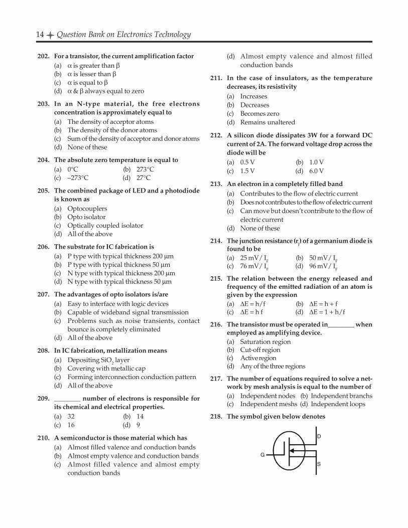
218. The symbol given below denotes
G
D
S
Electronic Materials and Devices 15
(a) n-channel depletion MOSFET(b) p-channel depletion MOSFET(c) n-channel enhancement MOSFET(d) p-channel enhancement MOSFET
219. The frequency biased PN junction diode(a) Acts like an open circuit(b) Offers infinite resistance(c) Provides very high voltage drop(d) Conducts current easily
220. The active components of the IC’s are formed in(a) The substrate (b) SiO2 layer(c) Epitaxial layer (d) None of these
221. The material whose Hall effect is found to be zero is(a) Conductor(b) Insulator(c) Extrinsic semiconductor(d) Intrinsic semiconductor
222. In a single chip computer, CMOS circuits are usedbecause of(a) Low lower dissipation(b) Large packing density(c) High noise immunity(d) economicity
224. In a transistor, if IC=100mA and IE=100mA thenthe value of βββββ is given by(a) 200 (b) 100(c) 10 (d) 1
225. The junction resistance (rj) of a Germanium diode is(a) 25 mV/IF (b) 50 mV/IF(c) 76 mV/IF (d) 96 mV/IF
226. ICBO doubles for energy 10°C rise in temperaturefor(a) Germanium(b) Silicon(c) Extrinsic Semiconductor(d) Both (a) & (b)
227. The nucleus of atom is made of(a) Protons & Electrons(b) Protons & Neutrons(c) Protons & Krypton(d) Neutron & Electrons
228. Widely used semiconductors such as silicon,germanium are placed in _____.(a) First column(b) Second column(c) Third column(d) Fourth column
229. Compare the Lists
List I List II(P) Pico (1) 10–12
(Q) Femto (2) 10–15
(R) Atto (3) 10–18
(S) Nano (4) 10–9
(a) P-(4), Q-(2), R-(3), S-(1)(b) P-(1), Q-(2), R-(3), S-(4)(c) P-(4), Q-(3), R-(2), S-(1)(d) P-(1), Q-(3), R-(2), S-(4)
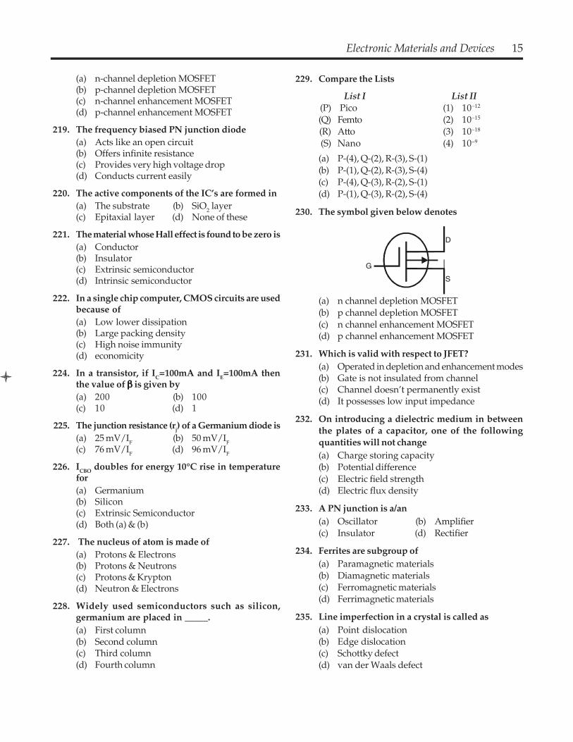
230. The symbol given below denotes
G
D
S
(a) n channel depletion MOSFET(b) p channel depletion MOSFET(c) n channel enhancement MOSFET(d) p channel enhancement MOSFET
231. Which is valid with respect to JFET?(a) Operated in depletion and enhancement modes(b) Gate is not insulated from channel(c) Channel doesn’t permanently exist(d) It possesses low input impedance
232. On introducing a dielectric medium in betweenthe plates of a capacitor, one of the followingquantities will not change(a) Charge storing capacity(b) Potential difference(c) Electric field strength(d) Electric flux density
233. A PN junction is a/an(a) Oscillator (b) Amplifier(c) Insulator (d) Rectifier
234. Ferrites are subgroup of(a) Paramagnetic materials(b) Diamagnetic materials(c) Ferromagnetic materials(d) Ferrimagnetic materials
235. Line imperfection in a crystal is called as(a) Point dislocation(b) Edge dislocation(c) Schottky defect(d) van der Waals defect
16 Question Bank on Electronics Technology
236. The elements in a periodic table are arranged,based on the increasing order of(a) Atomic number(b) Mass number(c) Molecular weight(d) Alphabetical order
237. For a silicon, the ICBO doubles for every(a) 5°C rise in temperature(b) 6°C rise in temperature(c) 10°C rise in temperature(d) 12°C rise in temperature
238. The conductor of a 10 km long, single phase, two-wireline is separated by a distance 1.5 m. The diameter ofeach conductor is 1 cm. If the conductors are of copper,the inductance of the circuit is found to be(a) 50.0 mH (b) 45.3 mH(c) 23.8 mH (d) 19.6 mH
239. An n-channel JFET having a pinch off voltage of–5 V shows a transconductance of 1 mA/V whenapplied gate-to-source voltage of –3 V. Then itsmaximum transconductance is found to be(a) 1.5 mA/V (b) 2.0 mA/V(c) 2.5 mA/V (d) 3.0 mA/V
240. Strictly speaking, for an NPN transistor,(a) IC should be positive but IE should be negative(b) IC should be negative but IE should be positive(c) Both IC & IE should be positive(d) Both IC & IE should be negative
241. Air gap in the iron core of an inductor prevents(a) Core saturation (b) Hysteresis loss(c) Flux leakage (d) Transformer action
242. The solid which has no periodic structures at all iscalled as(a) Crystalline solid(b) Amorphous solid(c) Polycrystalline solid(d) Solids
243. The resistivity of pure silicon decreases(a) With decrease in temperature(b) With increase in temperature(c) With constant temperature(d) None of these
244. JFET channel is pinched-off only when(a) VDD is equal to VP
(b) VDS is greater than VP
(c) VDS is less than VP
(d) VDS is equal to VP
245. Determine the invalid statement.(a) For an n-channel JFET, both VGS and VP are
negative(b) For a p-channel JFET, both VGS and VP are posi-
tive(c) For an n-channel JFET, IDSS is positive(d) For a p-channel JFET, IDSS is positive
246. The function of SiO2 layer in IC fabrication is(a) Oxide masking(b) Oxide passivation(c) Oxide purification(d) Both (a) & (b)
247. When gold and aluminum react, an intermetalliccompound is formed known as(a) Purple plaque (b) Yellow plaque(c) Red plaque (d) White plaque
248. A plasma is a(a) Collection of electrons, positive and negative
ions only(b) Collection of electrons and positive ions only(c) Collection of neutral atoms and molecules only(d) Collection of electrons, positive and negative
ions, neutral atoms and molecules
249. Which is the final step in wafer processingsequence?(a) Photolithography(b) Chemical vapour(c) Metallization(d) Oxidation
250. Diffusion constant for electron is ________ to hole.(a) Equal(b) Greater than(c) Lesser than(d) Can’t be determined
251. When a transistor is used as amplifier, then ______breakdown is more destructive to the device.(a) Zener (b) Diode(c) Collector-Base (d) Base-Emitter
252. The variation of IC with VCE observed in a bipolartransistor output characteristic is called as(a) Ohmic effect (b) Early effect(c) Late effect (d) Natural effect
253. Small signals refers to(a) Low amplitude signals(b) Low frequency signals
Electronic Materials and Devices 17
(c) Small signals as compared to bias currents(d) Small signals as compared to bias currents &
voltages in a circuit
254. Kirk effect in a transistor occurs when(a) The majority carrier’s concentration in the
collector becomes comparable to the donor-atom doping density
(b) The minority carrier’s concentration in thecollector becomes comparable to the acceptoratom doping density
(c) Emitter-base junction is reverse biased(d) The base region of transistor stretches into the
collector region of transistor
255. The parasitic resistance value can be reduced by(a) Operating the transistor in saturation region(b) Operating the transistor in cut-off region(c) Changing the transistor structure(d) Grounding the emitter terminal of the transistor
256. Consider the statements
Statement I: N-channel MOS transistors are fasterthan p-channel MOS transistor.
Statement II: Surface field effect is the operationalprinciple of MOSFETs.
Which of the above is/are a valid one?(a) Statement I only(b) Statement II only(c) Both statements I and II(d) Either statement I or II
257. Identify the ordered processing steps in fabricationof integrated circuits.(a) Diffusion, Oxidation, Chemical vapor
deposition, Photolithography, Metallization(b) Oxidation, Diffusion, Chemical vapor
deposition, Photolithography, Metallization(c) Chemical vapor deposition, Oxidation,
Diffusion, Photolithography, Metallization(d) Diffusion, Oxidation, Photolithography,
Chemical vapor deposition, Metallization
258. Parasitic resistance is produced by(a) Viruses(b) Infinite resistance of silicon(c) Finite resistance of impurity(d) Finite resistance of silicon between the top
contacts on the transistor and active base regionbeneath the emitter
259. {111} planes oxidize faster than {100} because(a) They have higher tensile strength(b) They have fewer atoms per unit surface area
(c) They have more atoms per unit surface area(d) They are good conductors
260. In IC fabrication, gettering is a process by which(a) The silicon wafer is highly polished(b) The silicon wafer is pre-heated to an optimum
temperature for diffusion(c) The harmful impurities or defects are removed
from the region in a wafer where devices are tobe fabricated
(d) Wafers are sliced into thin films
261. The law, which governs the diffusion processduring the IC fabrication, is(a) Flicker’s law (b) Flick law(c) Fick law (d) Fickler’s law
262. In order to increase the speed of digital operations,_______ is used as diffusant which reduces thecarrier life time.(a) Boron (b) Arsenic(c) Nickel (d) Gold
263. The most common diffusant used in interstitialdiffusion in IC fabrication is(a) Boron (b) Arsenic(c) Nickel (d) Gold
264. The volt-ampere relation for PN junction can beexpressed as(a) I = IS[e
V/n.Vt] –1(b) I = 1/IS[e
V/n.Vt] –1(c) I = IS[e
V/n.Vt –1](d) I = IS[e
V/n.Vt +1]
265. The velocity of the electron in the nth orbit is givenby the equation(a) Vn = (hn / πmrn)(b) Vn = (πh2 / mrn)(c) Vn = (n(h/2π)/ mrn)(d) Vn = (nh/2πmrn)
266. What is the de Broglie wavelength of neutrons atroom temperature?(a) 0.145 nm (b) 0.82 nm(c) 0.64 nm (d) 4.23 nm
267. Metallic crystal possesses(a) High optical reflection and absorption co-
efficient(b) Good conducting property due to the presence
of free electrons(c) Opaque to all electromagnetic radiations from
low frequency to the middle ultraviolet(d) All of these
18 Question Bank on Electronics Technology
268. Germanium has a(a) Diamond cube (dc) structure(b) Simple cube (sc) structure(c) Face centered cube (fcc) structure(d) Body centered cube (bcc) structure
269. Superconductivity is otherwise known as(a) Zero resistivity(b) Zero conductivity(c) Infinite resistivity(d) Simply semiconductor
270. The tunnel effect was discovered in 1960 by(a) H.K. Onnes (b) Deaver & Fairbank(c) J. Bardeen (d) Giaever
271. The unit of electrical dipole moment is(a) Debye(b) Pascal(c) Ohms(d) Flux
272. Superconductivity can be destroyed by theapplication of(a) An electrical field(b) A magnetic field(c) Both electrical & magnetic fields simulta-
neously(d) Either electric or magnetic field
273. The electron mobility is greater in(a) Germanium(b) Silicon(c) Gallium arsenide(d) Bakelite
274. The relative distance of the electron from thenucleus is same as(a) The relative distance between Earth and Moon(b) The relative distance between Sun and Earth(c) The relative distance between Earth and Pluto(d) The relative distance between Sun and Pluto
275. If an excess carrier is injected into semiconductor,(a) They diffuse away from the point of injection(b) They concentrate at the point of injection(c) They randomly move but centered at the point
of injection(d) They uniformly distribute themselves
276. One part of donor impurities to 108 parts ofgermanium(a) Increases the conductivity of the crystal two-
fold
(b) Increases the conductivity of the crystal four-fold
(c) Increases the conductivity of the crystal eight-fold
(d) Increases the conductivity of the crystal ten-fold
277. The following statement forms the basis of one ofthe following electronic devices. Identify it.
“If a particle is electronic on a potential barrierwith energy certainly less than the height of thepotential barrier, it will not necessarily be reflectedby the barrier but there is always a probability thatit may cross the barrier and continue its forwardmotion”.(a) Tunnel diode(b) PIN diode(c) Schottky diode(d) Metal oxide semiconductor diode
278. The Bragg’s diffraction equation is given by(a) sin θ = nλ / 2d(b) sin θ = n/2dλ(c) sin θ = 2dnλ(d) sin θ = 2(n–λd)
279. Silicon & carbon have a(a) Diamond cube (dc) structure(b) Simple cube (sc) structure(c) Face centered cube (fcc) structure(d) Body centered cube (bcc) structure
280. Which one of the following factors doesn’tcorrespond to a common collector amplifier?(a) High input impedance(b) Low output impedance(c) High voltage gain(d) High current gain
281. The gain of source follower is(a) 1 (b) 5(c) 10 (d) 100
282. Identify the false statement with respect to theZener diode.(a) Zener diode is needed for voltage regulation(b) Zener diode is operated in reverse biased
condition(c) Zener diode has similar characteristics to that
of an ideal current source(d) None of the above
Electronic Materials and Devices 19
283. Consider the statements:
Statement I: Fermi level is slightly lowered byadding the donor impurity
Statement II: Fermi level is the maximum energythat any electron can have at room temperature.Which of the following is correct?(a) Statement I(b) Statement II(c) Both statements I & II(d) Either statement I or II
284. GaAs LED’s emit radiation in the(a) Ultraviolet region(b) Visible region(c) Infrared region(d) Invisible region
285. LED’s are fabricated from(a) Si (b) Ge(c) Si or Ge (d) GaAs
286. Which material is generally used to build LED?(a) Compounds of gallium(b) Compounds of phosphorus(c) Compounds of germanium(d) Compounds of silicon
287. A UJT has(a) Negative resistance characteristics(b) Low firing current(c) Bipolar device(d) All of these
288. Breakdown in a silicon UJT was observed to occurat a voltage of 6V, for a VBB = 10V its stand off ratiois found to be(a) 1.66 (b) 0.60(c) 0.54 (d) 0.51
289. Which switching device was used in the firstgeneration computers?(a) Vacuum tubes (b) Transistors(c) IC’s (d) Diodes
290. Which of the following is not a merit of transistorsin place of vacuum tubes?(a) Transistors are compact(b) Consume less power(c) Faster and economical(d) None of these
291. Which diode is otherwise called as hot carrierdiode?
(a) Schottky diode(b) Tunnel diode(c) PIN diode(d) Varactor diode
292. Which one of the following devices is a unipolarone?(a) PIN diode(b) Zener diode(c) PN diode(d) Schottky diode
293. _______________ is another type of VVC diode.(a) PN junction diode(b) Step recovery diode(c) PIN diode(d) Schottky diode
294. Tunneling phenomena was invented by(a) Einstein (b) Henry Hill(c) Dr. Fresnel (d) Dr. Leo Easaki
295. An FET acts as(a) A variable resistor(b) A variable capacitor(c) A variable voltage source(d) A variable current source
296. The donor impurity must have only __________valence electrons.(a) 2 (b) 3(c) 4 (d) 5
297. A P-type germanium semiconductor is doped with(a) Gallium (b) Gold(c) Silver (d) Silicon
298. The Miller indices of the diagonal plane of a cubeare(a) 0 1 0 (b) 1 1 0(c) 0 0 1 (d) 1 1 1
299. The junction capacitance varies(a) Directly as square root of the voltage(b) Inversely as square root of the voltage(c) Directly as cube root of the voltage(d) Inversely as cube root of the voltage
300. Silicon diode is less suited for low voltage rectifieroperation because(a) Its breakdown voltage is low(b) It is costly(c) It is temperature dependent(d) Its breakdown voltage is high
20 Question Bank on Electronics Technology
301. A capacitor C charges to the applied voltage in(a) Three time constants(b) Five time constants(c) Six time constants(d) Ten time constants
302. A time constant is(a) A relative measure of time(b) An absolute measure of time(c) Not an absolute measure of time(d) Both (a) and (c)
303. It will take _______________ time constants todischarge the capacitor almost completely.(a) One (b) Two(c) Four (d) Five
304. A 0.25 microfarads capacitor is charged through a2.2 M Ohms resistor towards an applied voltageof 50 V. In one time constant, the capacitor wouldhave charged to(a) 11.6 V (b) 21.6 V(c) 31.6 V (d) 41.6 V
305. The phenomenon “conductivity modulation” isexhibited by(a) UJT (b) Diac(c) SCR (d) Triac
306. The intrinsic stand-off ratio is dependent on(a) Current carrying capacity of UJT(b) Geometry of UJT(c) Voltage handling capacity of UJT(d) Noise ratio
307. Between the peak point Vp and the valley pointVv of the static emitter characteristics the emittervoltage ________ as emitter current increases.(a) Increases(b) Decreases(c) Remains constant(d) Is zero
308. Cermets are(a) Inductive materials(b) Capacitive material, resistive materials(c) Resistive materials(d) Magnetic materials
309. One angstrom is equal to(a) 10–9 metre(b) 10–11 metre(c) 10–10 metre(d) 10–12 metre
310. The storage time of a P – N junction diode(a) Decreases with increased reverse bias voltage(b) Decreases with increased forward bias voltage(c) Increases with increased reverse bias voltage(d) None of these
311. The switching speed of a Schottky diode is(a) Lower than p-n junction diode(b) Same as p-n junction diode(c) Higher than p-n junction diode(d) Can’t define
312. The most commonly used configuration of an n-p-ntransistor as a switch is(a) Common collector(b) Common emitter(c) Common base(d) Both common base and common collector
313. N-P-N transistors are preferred ones than P-N-Ptransistors for digital application because(a) Electron mobility is more compared to holes
mobility(b) They are cheaper(c) They are costlier(d) Easy availability in the market
314. The Schottky diode is(a) A vacuum device(b) A metal – semiconductor device(c) Purely semiconductor device(d) MOS device
315. For a MOSFET the gate current(a) Is decedent on drain current(b) Increases with increase in drain voltage(c) Decreases with decrease in drain voltage(d) Is negligibly very small
316. The term “Baud Rate” is defined as(a) Rate at which parallel data transmission takes
place(b) Rate at which microprocessor operates(c) Rate at which parallel data are converted to
serial data(d) Rate at which serial data transmission takes
place
317. The gate voltage required for the conduction of ann-channel enhanced mode MOSFET having athreshold voltage of 2V is(a) 0 V (b) 1 V(c) 2 V (d) More than 2 V
Electronic Materials and Devices 21
318. A Schottky transistor used as a switch operatesbetween(a) Cut-off and saturation regions(b) Cut-off and active regions(c) Active and saturation regions(d) None of these
319. For a transistor operating in the saturation region(a) Ic ≤ hfe . IB (b) Ic > hfe . IB(c) Ic = hfe . IB (d) Ic = 0
320. Which one of the following is a uniquecharacteristic of Schottky transistor?(a) Lower propagation delay(b) Higher propagation delay(c) Lower power dissipation(d) Higher power dissipation
321. Higher switching speed is possible in Schottkytransistor than ordinary N-P-N transistor due to(a) It operates in cut-off and saturation regions(b) It operates in active and saturation regions(c) It is prevented from going into saturation(d) It is prevented from going into cut-off
322. Consider the statements
Statement I: The temperature coefficient ofresistance of a semiconductor is negative while thatof a metal is positive.
Statement II: A semiconductor behaves as aninsulator at 0°K while it has some conductivity atroom temperature.
Which of the following is/are correct?(a) Statement I(b) Statement II(c) Both statements I & II(d) Either statement I or II
323. When a transistor is turned from ON to OFF, thetransistor comes to OFF state,(a) Once the input signal is removed(b) As soon as the input signal is reversed(c) As soon as the power supply is switched off(d) After the excess charge stored in the base region
is removed.
324. The delay in the switching mode operation of a p-n junction diode is caused due to the(a) Metallic contact(b) Small size(c) Different doping levels at two sides of junction(d) Excess minority charge stored on the two sides
of the junction when it is forward biased.
325. An open input terminal of ECL gate(a) Will behave as if it is connected to logic high level(b) Will behave as if it is connected to logic low
level(c) Will assume same voltage between logic high
and low levels(d) Will assume a very high voltage causing
damage to the device.
326. With respect to semiconductor, identify the validstatement.I Drift and diffusion occur simultaneously in a
semiconductor device.II Mobility of free electrons is same as that of holes.III A crystal is not electrically neutral.IV Semiconductors exhibit negative temperature
coefficient.(a) I (b) II(c) III (d) IV
327. Which one is categorized as P-type impurity?(a) Arsenic (b) Boron(c) Bismuth (d) Antimony
328. Which one is categorized as N-type impurity?(a) Bismuth (b) Indium(c) Gallium (d) Boron
329. In which band(s) do the movements of electronsand holes take place?(a) Valence band(b) Conduction band(c) Conduction and valence bands respectively(d) Neither valence nor conduction band
330. The ratio of majority and minority carriers of anintrinsic semiconductor is(a) Zero (b) Infinity(c) Unity (d) Very large
331. The ratio of majority and minority carriers of anextrinsic semiconductor is(a) Zero (b) Infinity(c) Unity (d) Very large
332. Consider the statements given below
Statement I: In FET the generator current isproportional to the input voltage.
Statement II: In BJT, the generator current isproportional to the input current.Which of the following is valid?(a) Statement I(b) Statement II(c) Both statements I & II(d) Either statement I or II
22 Question Bank on Electronics Technology
333. Transconductance of JFET is given by
(a)ΔΔ
DS
D
VI (b)
(c) (d)
334. Ultraviolet radiation is used in IC fabrication for(a) Diffusion(b) Masking(c) Isolation(d) Metallization
335. FETs are used in an amplifier to obtain(a) Low input impedance(b) Low output impedance(c) High input impedance(d) High output impedance
336. Which of the following exhibits very high inputimpedance?(a) Diode (b) P-N-P(c) N-P-N (d) FET
337. Which one of the following materials does nothave a covalent bond?(a) Silver (b) Silicon(c) Organic polymer (d) Diamond
338. The device having scalar characteristics with thatof an ideal voltage source is(a) FET(b) P-N-P transistor(c) Zener diode(d) MOSFET
339. The device having closer characteristics with anideal current source is(a) Vacuum diode(b) Zener diode(c) UJT(d) Transistor in common base mode
340. A piece of copper and another of silicon are cooledfrom room temperature to 80ºK. The resistance of(a) Each of them increases(b) Each of them decreases(c) Copper increases and silicon decreases(d) Copper decreases and silicon increases
341. In a conductor, the valence band and the conductionband(a) Are separated by a small gap(b) Are separated by a large gap(c) Are overlapping(d) Don’t exist at all
342. The forbidden in germanium at 0°K is(a) 0.785 eV (b) 1.21 eV(c) 1.00 eV (d) 0.01 eV
343. Einstein’s relation is given by
(a)
(b)
(c)
(d)
344. Mobility of electron is highest in(a) Silicon (b) Germanium(c) Gallium arsenide (d) Carbon
345. The mean free path for electron drift increases with(a) Purity concentration(b) Strain hardening(c) Elastic modulus(d) Length
346. To make silicon P-type, one must add(a) Ge (b) Si(c) Sb (d) Ga
347. An N-type semiconductor as a whole is(a) Positively charged(b) Negatively charged(c) Electrically neutral(d) Can’t be defined
348. The peak inverse voltage is the maximum voltagethat can be applied to a diode without(a) Burning (b) Destruction(c) Overheating (d) Charging
349. As the temperature is increased the voltage acrossa diode carrying a constant current(a) Increases(b) Decreases(c) Remains constant(d) Alternately increases and decreases
350. The P-N junction diode is a(a) Passive device (b) Vacuum device(c) Unilateral device (d) Bilateral device
351. In an unbiased junction, the thickness of chargedepletion region is of the order(a) 0.005 μm (b) 0.5 μm(c) 5 μm (d) 10–10 m
Electronic Materials and Devices 23
352. In the symbol of transistor the arrow mark shows(a) Emitter (b) Collector(c) Base (d) Gate
353. The input resistance of a common amplifier tran-sistor is of the order(a) 1 MΩ (b) 1 kΩ(c) 0.01 Ω (d) 0.001 Ω
354. The output characteristics curve of a transistor ismuch more like those of(a) A diode (b) A tetrode(c) A triode (d) A pentode
355. The gain of a voltage follower is(a) Greater than 1(b) Lesser than 1(c) Equal to 1(d) Slightly less than 1
356. Lowest output resistance is obtained in(a) CB (b) CE(c) CC (d) None of these
357. Transistor is a(a) Current controlled current device(b) Current controlled voltage device(c) Voltage controlled current device(d) Voltage controlled voltage device
358. The temperature coefficient of a Zener diodechanges from negative to positive(a) Below 5 V(b) Above 6 V(c) Between 5 V and 6 V(d) Exactly at 0 V
359. In an unbiased semiconductor junction, thejunction current at equilibrium is(a) Zero because equal and opposite charges are
crossing the junction(b) Zero because no charges are crossing the
junction(c) Due to diffusion of minority carriers(d) Due to diffusion of majority carriers
360. Due to thermo-ionic emission, the weight of themetal piece(a) Increases(b) Decreases(c) Remains the same(d) Varies but can’t define
361. Boltzmann diode equation relates(a) Voltage and temperature characteristics of a
junction(b) Voltage and current characteristics of a
junction(c) Current and temperature characteristics of a
junction(d) Resistance and temperature characteristics of
a junction
362. Which of the following is an active device?(a) Electric bulb(b) Loudspeaker(c) Transformer(d) None of the above
363. The main application of the enhancement modeMOSFET is(a) Amplification(b) Switching(c) Tuningd) Rectification
364. ___________ indicates how effectively the inputvoltage controls the output current in a JFET.(a) Slow rate(b) Transconductance(c) Transresistance(d) Intrinsic stand-off ratio
365. Transconductance is measured in(a) Mho (b) Volts(c) Amperes (d) Ohms
366. _________ is preferred form of bias for a JFETamplifier.(a) Self bias(b) Voltage divider bias(c) Two supply bias(d) Emitter feedback bias
367. Transconductance is basically a/an(a) AC quantity(b) DC quantity(c) Either AC or DC quantity(d) None of these
368. An ordinary resistor connected across a circuit canbe considered as(a) An active load(b) A passive load(c) A switching device(d) Three terminal device
24 Question Bank on Electronics Technology
369. The transconductance JFET at the Q-point is_________ the maximum transconductance whichoccurs when Vds = 0.(a) Less than(b) Greater than(c) Equal to(d) None of the above
370. The main advantage of cascade amplifier is(a) Low input resistance(b) Low input capacitance(c) High output resistance(d) High output capacitance
371. A current regulator diode is basically a(a) Zener diode(b) MOSFET(c) JFET whose gate and source are tied up(d) Transistor
372. _________ is an excellent device for interfacingdigital IC’s to high power loads.(a) Depletion mode power MOSFET(b) Enhancement mode power MOSFET(c) JFET(d) Bipolar transistor
373. VMOS transistor exhibits(a) Negative thermal coefficient(b) Positive thermal coefficient(c) Zero thermal coefficient(d) None of the above
374. VMOS transistor can shut off amperes of current in(a) Few milli seconds(b) Few seconds(c) Few microseconds(d) Tens of nanoseconds
375. The merits of VMOS transistors as compared tobipolar transistor is/are(a) No extra changes are stored while in induction(b) Cannot go into thermal run away(c) Exhibits negative temperature coefficient(d) All of the above
376. VMOS transistor is basically(a) Power transistor(b) Three diodes connected parallelly(c) JFET(d) Enhanced-mode MOSFET
377. A JFET has(a) One built-in diode(b) Two built-in diodes
(c) Three built-in diodes(d) Four built-in diodes
378. The JFET acts as a ____________ along thehorizontal part of the drain curve.(a) Resistor(b) Current source(c) Voltage source(d) Current sink
379. The JFET acts as a _______ along vertical parts ofthe drain curve.(a) Resistor (b) Current source(c) Voltage source (d) Current sink
380. The transconductance curve of JFET which is alsocalled as square law curve is(a) Straight line (b) Parabolic(c) Circular (d) Wavy
381. Which of the following is/are valid statement(s)?I The gate of a JFET is forward biased hence acts
as a voltage controlled deviceII The gate of a JFET is reversed biased, hence
acts as a voltage controlled deviceIII The gate of a JFET is reverse biased, hence acts
as voltage controlled device(a) I (b) II(c) I and II (d) I, II and III
382. The point above the drain voltage, where there isno increase in drain current in a JFET is called as(a) Breakdown point(b) Pinch off point(c) Knee point(d) Critical point
383. The depletion region is one which has(a) Immobile charges(b) Mobile charges(c) Atoms(d) Molecules
384. Constantan is a/an(a) Alloy (b) Metal(c) Nonmetal (d) Isotope
385. The nature of atomic bond found in diamond is(a) Tetravalent(b) Covalent(c) Metallic(d) Ionic
Electronic Materials and Devices 25
386. The conductivity of a P-type semiconductor is(a) σ = q μoP (b) σ = q μo(c) σ = q μon (d) σ = q p
387. The gate cut-off and pinch-off voltages of JFET have(a) Same magnitude and sign(b) Different magnitudes but same sign(c) Same magnitude but different signs(d) Different magnitudes and signs
388. The pinch-off voltage of JFET has a samemagnitude as that of(a) Gate voltage(b) Gate source voltage(c) Drain–source voltage(d) None of these
389. The current gain of a transistor is(a) The ratio of collector current to emitter current(b) The ratio of collector current to base current(c) The ratio of base current to collector current(d) The ratio of emitter current to collector current
390. The base current of a transistor is typically(a) Less than emitter current(b) Greater than emitter current(c) Same as emitter current(d) Equal to the sum of emitter and collector
currents
391. The free electrons have ___ in the base region of atransistor.(a) Short lifeterm (b) Long lifeterm(c) No lifeterm at all (d) Infinite lifeterm
392. The free electrons recombine with a hole in thebase region of a transistor to become(a) Free electrons (b) Valence electrons(c) Atom (d) Majority carrier
393. A transistor acts as a(a) Diode and voltage source(b) Diode and current source(c) Diode and power supply(d) Diode and resistance
394. The knee voltage of a PN junction diode is ap-proximately equal to the(a) Forward voltage(b) Applied voltage(c) Breakdown voltage(d) Potential
395. The capacitance of a varactor diode increases,when the reverse voltage across it is(a) Decreased(b) Increased
(c) Kept constant(d) None of the above
396. A Zener diode(a) Is a battery under forward biased condition(b) Acts like battery when it breakdowns(c) Is a switch(d) Is a device having barrier potential more than 5V
397. A back diode(a) Is ordinary Zener diode(b) Is used to rectify strong signals(c) Conducts better in the forward than in the
reverse directions(d) Is used to rectify weak signals whose peak
amplitudes are between 0.1 V and 0.7 V
398. Exposure of insulating material to moisture causesan increase in(a) Dielectric loss(b) Dielectric constant(c) Dielectric strength(d) Insulation resistance
399. Cu2MnAl is a(a) Semiconductor(b) Ferrimagnetic material(c) Paramagnetic materialD) Ferromagnetic material
400. Soft magnetic material is(a) Tungsten steel (b) Alcomax(c) Bismuth (d) Iron
401. Ferrimagnetic materials are generally used as(a) Conductors(b) Insulators(c) Semiconductors(d) Resistors
402. Identify N-type impurity from the following(a) Fe (b) Ga(c) Sb (d) B
403. Which one of the following is a superconductivematerial?(a) Gold (b) Silver(c) Mercury (d) Copper
404. Facing fraction of simple cube is(a) 6.48 (b) 0.52(c) 0.65 (d) 0.89
405. Air exhibits(a) Ferromagnetism(b) Ferrimagnetism(c) Paramagnetism(d) Antiferromagnetism
26 Question Bank on Electronics Technology
406. The main advantage of a point contact diode isthat(a) The ratio of forward current to reverse current
is very high(b) Low input impedance(c) Its cut-in voltage is equal to zero(d) Its reverse resistance is infinite
407. Match the lists.
List I List II(Band gap in eV) (Material)
A. 0.67 1. GaAsB. 1.1 2. Cadmium sulphateC. 1.4 3. SiliconD. 2.4 4. Germanium
(a) A-4, B-3, C-1, D-2(b) A-3, B-2, C-1, D-4(c) A-4, B-1, C-3, D-2(d) A-2, B-3, C-1, D-4
408. Match the given lists.
List I List II(Name of the device) (Application)A. Diode 1. RectificationB. Tunnel diode 2. Microwave switchingC. Zener diode 3. As oscillatorD. PIN diode 4. Voltage stabilization(a) A-1, B-3, C-4, D-2(b) A-1, B-4, C-3, D-2(c) A-1, B-2, C-4, D-3(d) A-2, B-4, C-3, D-1
409 The output characteristics of a JFET is similar to(a) Triode (b) Pentode(c) Thyratron (d) Tetrode
410. Internal heating in a capacitor is mainly due to(a) Dielectric charge(b) Leakage resistance(c) Electron movement(d) Plate dimension
411. The capacitance of a parallel plate capacitor is notaffected by(a) Area of plates(b) Dielectric medium(c) Distance between the plates(d) Thickness of the plates
412. According to Coulomb’s first law(a) Like charges attract each other(b) Like charges repel each other
(c) There is no force between the charges(d) None of these
413. Varistors are(a) Carbon resistors(b) Rheostats(c) Non linear resistors(d) Potentiometers
414. Resistivity of a semiconductor depends upon(i) Atomic structure of the semiconductor(ii) Shape of the semiconductor(iii) Length of the semiconductorOf these statements(a) (i) is correct(b) (ii) is correct(c) (iii) is correct(d) (i) and (iii) are correct
415. The impurity atoms in semiconductors(a) Inject more charge carriers(b) Reduce the energy gap(c) Increase the kinetic energy of valence electrons(d) All of the above
416. The Hall angle of a metal sample is(a) Independent of the magnetic flux density B(b) Independent of the carrier mobility(c) Independent of the density of free carriers(d) Dependent on magnetic flux density
417. ICBO in a transistor can be reduced by(a) Reducing IB
(b) Reducing VCC
(c) Reducing IE
(d) Reducing the temperature
418. Mass of a proton is(a) 1.67 × 10⁻²⁴ kg (b) 1.67 × 10⁻²⁵ kg(c) 1.67 × 10⁻²⁶ kg (d) 1.67 × 10⁻²⁷ kg
419. The kinetic energy of a bounded electron is____________ that of an unbounded electron.(a) Less than (b) Twice than(c) Greater than (d) Same as
420. Superconductivity is due to(a) All electrons having Fermi energy at 0º K(b) All electrons interacting in the super
conducting state(c) Crystal structure having no atomic vibration
at 0º K(d) Crystal structure having infinite atomic
vibration at 0º K
Electronic Materials and Devices 27
421. A linear resistor is a(a) Current controlled resistor(b) Voltage controlled resistor(c) Both (a) and (b)(d) Neither (a) nor (b)
422. A capacitor with no initial charge at t=μ acts as a(a) Short circuit (b) Open circuit(c) Voltage source (d) Current source
423. Donor type impuritiesi. Have five valence electronsii Create excess free electronsiii Are used to make n-type semiconductorsiv Have three valence electrons
Of these statements(a) i and iv are correct(b) i, ii and iii are correct(c) ii, iii and iv are correct(d) iii and iv are correct
424. Ionic bond in solid depends on(a) Transfer rate of electrons(b) Sharing of electrons(c) Electric dipole(d) All of the above
425. A material is said to be superconductive when itsresistance is
(a) Infinity (b) Zero(c) Negative (d) Very small
426. The type of bonding observed in graphite is
(a) Metallic (b) Covalent(c) van der Waals (d) Both (b) and (c)
427. The temperature at/beyond which ferroelectricmaterials lose their ferroelectric properties iscalled as
(a) Curie temperature(b) Absolute temperature(c) Inversion temperature(d) Critical temperature
428. Ferro-electric materials are widely used as_________ transducers.
(a) Active(b) Passive(c) Electromechanical(d) Crystal
429. Match the items given in list I with those in list II.
List I List II(Materials) (Forbidden energy gap)
(A) Conductors 1. Large eV(B) Insulators 2. Zero eV(C) Germanium 3. 1.12 eV(D) Silicon 4. 0.72 eV(a) A-4, B-3, C-1, D-2(b) A-2, B-1, C-3, D-4(c) A-1, B-2, C-4, D-3(d) A-2, B-1, C-4, D-3
430. Identify the wrong statementsi. Asbestos is least hygroscopicii. Asbestos is used as insulation in high voltage
installationsiii. Asbestos are neither mechanically strong nor
flexible(a) i (b) ii(c) iii (d) i and iii
431. Barium titanate is a(a) Piezo-electric material(b) Ferro-electric material(c) Semiconductor material(d) Both piezo-electric and ferro-electric material
432. Insulation used in commutator is(a) Wood (b) PVC(c) Mica (d) Glass
433. Dielectric materials are essentially(a) Insulating materials(b) Ferro-electric materials(c) Ferri-electric materials(d) Superconducting materials
434. The property of bakelite is/are(a) Hardness(b) Uncombustibility(c) Highly inflammable(d) Both (a) and (b)
435. Hysteresis loss is(a) Proportional to f(b) Proportional to 1/f(c) Proportional to f2
(d) Proportional to 1/f2
436. The magnetic material employed for VHFapplication is(a) Silicon steel (b) Alnico(c) Cobalt salt (d) Ferrite
28 Question Bank on Electronics Technology
437. Soft magnetic material is(a) Tungsten steel (b) Iron(c) Alcomax (d) Bismuth
438. Piezo-electricity is observed in(a) Mica (b) Nickel(c) Glass (d) Quartz
439. Rochelle salt, a peizo-electric crystal has(a) One curie point(b) Two curie points(c) Three curie points(d) No curie point
440. Basically iron is a(a) Ferro-magnetic material(b) Ferri-magnetic material(c) Para-magnetic material(d) Anti-ferromagnetic material
441. A 0ºK, germanium acts as(a) Insulator(b) Superconductor(c) Dielectric(d) Semiconductor
442 With the fall in temperature, the receptivity ofmetals normally(a) Increases(b) Tends to be zero(c) Remains unchanged(d) Decreases first and then increases
443 The transport phenomenon in conductor is due to(a) Electric field(b) Magnetic field(c) Electro-magnetic field(d) None of the above
444. Power loss in an electrical circuit can take place in(a) Inductance only(b) Capacitance only(c) Resistance only(d) Inductance and resistance
445. The dynamic resistance of a parallel resonantcircuit is given by(a) LC/RL (b) LCRL(c) C/LRL (d) L/CRL
446. A choke coil of inductance L and series resistanceR is shunted by a capacitor C. The dynamicimpedance of the resonant circuit would be
(a) R/LC (b) C/RL(c) L/RC (d) 1/RLC
447. A series R-C circuit is suddenly connected to a dcvoltage of V volts. The current in the series cir-cuit just after the switch is closed is equal to(a) Zero (b) V/RC(c) VC/R (d) V/R
448. A series RL circuit with R = 100 ohms, L = 50 Hz issupplied to a dc source of 100V. The time taken forthe current to rise 70% of its steady state value is(a) 0.3 seconds (b) 0.6 seconds(c) 0.9 seconds (d) 1.0 seconds
449. A capacitance C is charged through a resistance R,the time constant of the charging circuit is givenby(a) R/C (b) 1/RC(c) RC (d) C/R
450. With the increase in temperature, the resistanceof the carbon(a) Increases (b) Decreases(c) Remains same (d) Becomes zero
451. On placing a dielectric in an electric field, thefield strength(a) Increases (b) Decreases(c) Remains constant (d) Reduces to zero
452. Coulomb’s law for the force between electriccharges most closely resembles with(a) Newton’s law of motion(b) Law of conservation of energy(c) Gauss theorem(d) Newton’s law of gravitation
453. Tunnel diode is(a) Linear resistor(b) Current dependent resistor(c) Voltage dependent resistor(d) Non-linear resistor
454. A UJT has(a) Anode, cathode and gate(b) Two anodes and one gate(c) Emitter, base and collector(d) One emitter and two bases
455. Vulcanized rubber(a) Is produced from trans-polyisoprene(b) Is also known as neoprene(c) Contains 20% of sulphur(d) Is produced from cis-polyisoprene
Electronic Materials and Devices 29
456. Thermoplastic and thermoset polymers differ in(a) Electrical properties(b) Glass transition temperature(c) Mechanical properties(d) Thermal properties
457. The acceptor atoms in a P-type semiconductor atnormal temperature(a) Carry a positive charge(b) Carry a negative charge(c) Are neutral(d) Are ions
458. Electroid transformation in alloys is ______reaction(a) Solid to solid (b) Solid to liquid(c) Liquid to solid (d) Liquid to liquid
459. Photoluminescence which persists for someperiod after excitation is known as(a) Phosphorescenceb) Tri-luminescence(c) Fluorescence(d) Bioluminescence
460. Germanium photodiodes have dark currents inthe order of(a) 5 mA (b) 10 mA(c) 25 mA (d) 10 A
461. Which one of the following is a Square law device?(a) Zener diode (b) Crystal diode(c) Tunnel diode (d) Varactor diode
462. A PIN diode is(a) A metal semiconductor diode(b) A microwave switch(c) A microwave detector(d) None of these
463. One of the following microwave diodes is suitablefor very low power oscillators(a) Tunnel diode(b) Gunn diode(c) PIN diode(d) Zener diode
464. Charge on the capacitor is(a) directly related to voltage and inversely related
to capacitance(b) directly related to capacitance and inversely
related to voltage(c) directly related to both voltage and capacitance(d) Inversely proportional to both voltage and
capacitance
465. Dielectric constant relates to(a) Comparative charge stored for a given material
versus air(b) The fact that the dielectric doesn’t have charge
characteristics(c) The insulating properties of the non-
conducting mediums(d) None of the above
466. Since dielectric materials are nonconductive(a) Capacitors leakage resistance is finite(b) Capacitors leakage resistance is infinite(c) A capacitor cannot pass current through the
circuit(d) None of the above
467. In a series dc circuit containing both a resistor anda capacitor, as the capacitor charges(a) The voltage across the resistor decreases(b) The voltage across the resistor increases(c) The voltage across the resistor remains
unaffected(d) None of the above
468. Active devices used in digital circuit generallyoperate as(a) Amplifiers(b) Switches(c) Rectifiers(d) Wave form generators
469. The devices commonly used for making digitalcircuits are(a) Mechanical switches(b) Relays(c) Vacuum tubes(d) Semiconductor devices
470. The time required to switch a P-N junction fromON to OFF is equal to(a) Zero (b) Storage time(c) Switching time (d) Transition time
471. The storage time of a p-n junction(a) Decreases with increased reverse-bias(b) Decreases with increased forward-bias(c) Increases with increased reverse-bias(d) Increases with increased forward-bias
472. The maximum operating frequency of a diodewhen used as a switch(a) Depends on the diode characteristics and
switching voltages(b) Depends on switching voltages(c) Depends on diode characteristics(d) None of the above
30 Question Bank on Electronics Technology
473. Fast switching of P-N junction requires(a) A large current in reverse direction(b) Zero current in reverse direction(c) Reverse saturation current in reverse direction(d) None of the above
474. For fastest switching operation, it is preferable touse(a) P-N junction diode(b) Vacuum diode(c) Zener diode(d) Schottky diode
475. The most commonly used configuration oftransistor as switch is(a) CB (b) CC(c) CE (d) CB or CC
476 When used as switch, a Schottky transistorswitches between(a) Cut-off and active regions(b) Cut-off and saturation regions(c) Active and saturation regions(d) Different operation points in the active region
477. In switching application, CE configuration ispreferred because(a) It requires low voltage(b) It requires only one power source(c) Of easier construction(d) Of negligible reverse saturation current
478. BJT with hfe =200, Ib =10 mA and IC= 4 mA isoperating in(a) Active region (b) Cut-off region(c) Saturation region (d) None of these
479. Schottky transistors are preferred over normaltransistors in digital applications because of their(a) Higher propagation delay(b) Higher power dissipation(c) Lower propagation delay(d) Lower power dissipation
480. For a MOSFET, the gate current(a) Is dependent on drain current(b) Is negligibly small(c) Is independent of gate voltage(d) Increases with increase in gate voltage
481. For an n-channel enhancement mode MOSFET,the drain current(a) Decreases with increases in drain voltage(b) Decreases with decrease in drain voltage(c) Increases with increases in gate voltage(d) Increases with decrease in gate voltage
482. The delay in the switching mode operation of a p-n junction diode is mainly due to(a) Metallic contacts(b) Different doping levels(c) Minority charge storage in the junction during
forward biased condition(d) Majority carriers in forward biased condition
483. When separation between two charges isincreased, the potential energy(a) Increases(b) Decreases(c) Remains constant(d) Either (a) or (b)
484. The saturation current in a diode depends upon(a) Plate voltage(b) Cathode temperature(c) Cathode material(d) Separation between cathode and plate
485. At zero kelvin, a piece of germanium becomes(a) Semiconductor (b) Good conductor(c) Bad conductor (d) None of these
486. When an N-P-N transistor is used as an amplifierthen(a) Electrons move from base to collector(b) Electrons move from emitter to base(c) Electrons move from collector to base(d) Holes move from base to emitter
487. In a semiconductor crystal, if the current flows dueto breakage of crystal bonds, then the semicon-ductor is called(a) Acceptor(b) Donor(c) Intrinsic semiconductor(d) Extrinsic semiconductor
488. If a transistor emitter current is 2mA, the collectorcurrent is(a) Greater than 2 mA(b) Less than 2 mA(c) Equal to 2 mA(d) Equal to 4 mA
489. A photodiode is used in reverse bias because(a) Majority of electron-hole pairs swept are
reversed across the junction(b) Only one side is illuminated(c) Reverse current is small compared to photo-
current(d) Reverse current is large compared to
photocurrent
Electronic Materials and Devices 31
490. In a phototransistor, the base current is(a) Set by a bias voltage(b) Directly proportional to light(c) Inversely proportional to light(d) Square to light intensity
491. A laser diode can be fabricated using(a) Germanium(b) Silicon(c) Gallium arsenide(d) Gallium phosphide
492. The general condition for a phototransistor is(a) Common base configuration(b) Common collector configuration(c) Common emitter configuration(d) Darlington-pair configuration
493. When a phototransistor is reverse biased, is keptin dark condition, the current flowing through thedevice corresponds to(a) Zero current(b) Reverse saturation current(c) Maximum flow of device current(d) Minimum flow of device current
494. Which of the following devices is suitable for verylow power oscillator circuit only?(a) TRAPATT diode (b) IMPATT diode(c) Gunn diode (d) Tunnel diode
495. The transferred-electron bulk effect occurs in(a) Germanium(b) Gallium arsenide(c) Silicon(d) Metal-semiconductor junction
496. The colour of an LED can be changed by(a) Using different band gap semiconductors(b) Varying the doping level of the semiconductor(c) Increasing applied voltage(d) None of the above
497. A Ge atom contains(a) Four valence electrons(b) Six valence electrons(c) Four protons(d) Six protons
498. At 25ºC, a Zener diode rates at 2 watts, its powerrating at 50ºC will be(a) Zero watts(b) Less than 1 watt
(c) Greater than 2 watts(d) Less than 2 watts
499. In any conductor, Hall voltage VH, is(a) Directly proportional to B(b) Directly proportional to 1/B(c) Directly proportional to B2
(d) Directly proportional to 1/B2
500. Drift current in germanium is caused by(a) Concentration gradient of charge carriers(b) Thermal agitation of crystal lattice(c) Incidence of light energy(d) Applied electric field
501. In a given semiconductor, Fermi level E is propor-tional to (n=total number of free electrons perunit volume).(a) n (b) n1/2
(c) n2/3 (d) n4/3
502. FET has offset voltage of about(a) 0.2 volts (b) 0.6 volts(c) 1.0 volts (d) 3.6 volts
503. At 300ºK, the forbidden energy gap in germanium is(a) 0.543 eV (b) 0.632 eV(c) 0.72 eV (d) 0.89 eV
504. Semiconductors in pure form are poor conductorsbecause(a) They have no valence electrons(b) All valence electrons are in electron pairs(c) They have a large number of holes(d) They have fewer electrons than protons
505. When a pure semiconductor is heated(a) It becomes metal(b) Its atomic structure collapses(c) Its resistance increases(d) Its resistance decreases
506. In a pure semiconductor, electric current is due to(a) Holes(b) Electrons(c) Both holes and electrons(d) Valence electrons
507. Merit of four-point probe method of determiningresistivity is that(a) It needs very small current(b) It gives the average resistivity(c) It gives the resistivity at a localized region of
the sample(d) It gives the exact resistivity of the bulk sample
with respect to voltage variations
32 Question Bank on Electronics Technology
508. The n type impurity(a) Can be added to Ge but not to Si(b) Can be added to Si but not to Ge(c) Creates excess holes(d) Creates excess electrons
509. Resistivity of semiconductor depends on(a) The length of the specimen(b) Cross-sectional area of the specimen(c) Volume of the specimen(d) Atomic nature of the semiconductor
510. A hole is the vacancy created when(a) Free electron moves on application of electric
field(b) An electron breaks its covalent bond(c) An atom core moves(d) An electron reverts from conduction band to
valency band
511. When a free electron is recaptured by a hole, theprocess is called(a) Diffusion (b) Restoration(c) Recombination (d) Drift
512. P-type semiconductor is(a) Positively charged(b) Electrically neutral(c) Negatively charged(d) Both (a) and (b)
513. An n-type semiconductor is(a) Positively charged(b) Negatively charged(c) Both (a) and (b)(d) Electrically neutral
514. LEDs fabricated from gallium arsenide emitradiation in the(a) Visible range(b) Infrared region(c) Ultraviolet region(d) Ultrasonic region
515. At room temperature, resistivity of pure silicon isexpressed as(a) 230 Ohms-cm(b) 2300 Ohms-cm(c) 23000 Ohms-cm(d) 230000 Ohms-cm
516. Valence electrons are found(a) In the nucleus(b) In the innermost shell(c) In the outermost shell(d) As free electrons in an atom
517. The diffusion constant for holes in germanium isfound to be(a) 13 cm2/s (b) 28 cm2/s(c) 32 cm2/s (d) 47 cm2/s
518. The relative dielectric constant of silicon is(a) 6 (b) 10(c) 12 (d) 14
519. In semiconductor, the rate of diffusion of chargecarriers depends on(a) Concentration gradient(b) Mobility(c) Both (a) and (b)(d) Either (a) or (b)
520. In p-type semiconductor(a) n=p (b) p<n(c) n<p (d) p>>n
521. When an atom loses one electron,(a) It becomes positive ion(b) It becomes negative ion(c) It becomes neutral(d) It also loses one proton
522. At 300ºK, the forbidden energy gap in silicon is(a) 0.78 eV (b) 1.21 eV(c) 0.72 eV (d) 1.10 eV
523. An intrinsic semiconductor at absolute zerotemperature(a) Acts as a good conductor(b) Acts as a good insulator(c) Has only few holes and electrons(d) Has only few holes but no electrons
524. Unijunction transistor(a) Is a bulk semiconductor device(b) Has two p-n junctions(c) Is a unipolar device(d) Has one p-n junction
525. In Schottky barrier diode, conduction is(a) Entirely by electrons(b) Entirely by holes(c) Mainly by electrons and partially by holes(d) Mainly by holes and partially by electrons
526. Identify from the following, the diode whichdoesn’t exhibit negative resistance characteristics.(a) Gunn diode(b) Tunnel diode(c) LSA diode(d) IMPATT diode
Electronic Materials and Devices 33
527. The major application of tunnel diode is(a) As voltage controllable device(b) As switching device in digital circuits(c) As oscillator(d) As rectifier
528. Energy required to break a covalent bond in asemiconductor is(a) Equal to 1.6 eV(b) Greater in Ge than in Si(c) Equal to the width of the forbidden energy
gap(d) None of the above
529. Temperature coefficient of resistance of a puresemiconductor specimen is(a) Zero (b) Positive(c) Negative (d) None of the above
530. Forbidden energy gap between the valence bandand conduction band is least in the case of(a) Impure silicon (b) Pure silicon(c) Pure germanium (d) Mica
531. In germanium an electron in the conduction band(a) Has same energy as an electron in valence band(b) Has less energy as compared to an electron in
valence band(c) Has greater energy as compared to an electron
in valence band(d) Has zero charge
532. In UJT, the value of stand-off ratio is(a) 0.2 (b) 0.4(c) 0.7 (d) 0.9
533. Zener breakdown results due to(a) Strong electric field across the junction(b) Thermal decomposition(c) Impact ionization(d) Emission of free electrons
534. ________ utilizes the cumulative multiplicationprinciple of carriers through field i n d u c e dimpact ionization.(a) Zener diode(b) Varactor diode(c) PIN diode(d) Avalanche diode
535. Tunnel diode is basically a junction diode with(a) High doping in p region alone(b) High doping in n region alone(c) High doping in both p and n regions
(d) Low doping in both p and n regions
536. In a tunnel diode, depletion layer width is of theorder(a) 100 Angstroms (b) 0.1 Micron(c) 1 Micron (d) 5 Microns
537. On increasing the current through the Zener diodeby a factor of 2, the voltage across the diode(a) Gets doubled(b) Becomes 4 times(c) Becomes half(d) Remains the same
538. The dynamic resistance of a Zener diode(a) Increases with increase in current(b) Decreases with increase in current(c) Decreases with decrease in current(d) Is independent of variation in current
539. In n-type germanium with boron impurity, theionization energy is about(a) 0.002 eV (b) 0.010 eV(c) 0.100 eV (d) 1.000 eV
540. In p-type semiconductor(a) Holes form the majority carrier(b) Free electrons form the minority carrier(c) Hole density is equal to electron density(d) It is formed by adding pentavalent impurity
541. In an intrinsic semiconductor, Fermi levelrepresents the energy level with probability ofits occupation of(a) 0 per cent (b) 25 per cent(c) 50 per cent (d) 75 per cent
542. In germanium, medium doping corresponds toimpurity of the order(a) 1 part in 105 (b) 1 part in 104
(c) 1 part in 103 (d) 1 part in 102
543. Forbidden energy gap between the valence andconduction bands is least in the case of(a) Pure Si (b) Pure Ge(c) Mica (d) Impure Si
544. Hole in a lattice is defined as(a) Free proton(b) Free neutron(c) Acceptor ion(d) Vacancy created by removal of electron from
covalent bond.
34 Question Bank on Electronics Technology
545. In germanium, when atoms are held together bythe sharing of valence electrons(a) Each shared atom leaves a hole(b) Valence electrons are free to move away from
the nucleus(c) They form reversible covalent bonds(d) They form irreversible covalent bonds
546. Seed crystal used in crystal growth is(a) A small crystal formed out of epitaxial growth(b) A signal crystal with a specific orientation(c) A signal crystal containing acceptor impurity(d) A signal crystal containing donor impurity
547. Crystal structure possessing imperfection causes(a) Increased mobility(b) Decreased mobility(c) Increased conductivity(d) Decreased conductivity
548. Through repeated zone refining, the residualimpurity in a semiconductor is of the order(a) 1 part in 104 (b) 1 part in 107
(c) 1 part in 109 (d) 1 part in 1011
549. Purification of silicon is difficult because of(a) Its high surface tension(b) Its crystalline nature(c) Its high melting point(d) Its high resistivity
550. The conduction band(a) Has same energy as forbidden band(b) Is a range of energies corresponding to the free
electrons(c) Is seen very close to forbidden band(d) None of these
551. Which is the initial process to be followed inpreparing devices from a semiconductor block?(a) Crystal formation (b) Crystal pulling(c) Purification (d) Wafering
552. Epitaxial growth is best suited for(a) Growing polycrystalline pure silicon(b) Growing crystal of several inch thickness(c) Very thick single crystal on a substrate(d) Very thin single crystal on a substrate
553. Excess majority carriers are the carriers which are(a) Equal to the number of hole concentration(b) In excess of the equilibrium number(c) Minority carriers in P-type semiconductor(d) Thermally generated
554. At room temperature intrinsic carrier concentrationis higher in germanium than in silicon due to(a) Larger atomic number(b) Greater atomic weight(c) High carrier mobility(d) Smaller energy gap
���
Electronic Materials and Devices 35
ANSWERS
1. (a) 2. (a) 3. (c) 4. (b) 5. (c) 6. (c) 7. (d) 8. (d)9. (b) 10. (c) 11. (a) 12. (d) 13. (b) 14. (d) 15. (d) 16. (a)
17. (b) 18. (d) 19. (a) 20–(b) 21. (c) 22. (b) 23. (b) 24. (a)25. (b) 26. (a) 27. (c) 28. (b) 29. (a) 30. (c) 31. (a) 32. (c)33. (d) 34. (c) 35. (d) 36. (c) 37. (b) 38. (c) 39. (b) 40. (d)41. (c) 42. (c) 43. (b) 44. (d) 45. (a) 46. (a) 47. (d) 48. (d)
49. (b) 50. (c) 51. (a) 52. (c) 53. (a) 54. (b) 55. (c) 56. (a)57. (b) 58. (c) 59. (a) 60. (c) 61. (d) 62. (d) 63. (c) 64. (a)65. (a) 66. (c) 67. (d) 68. (b) 69. (b) 70. (b) 71. (c) 72. (d)73. (a) 74. (c) 75. (d) 76. (a) 77. (b) 78. (d) 79. (d) 80. (b)81. (d) 82. (d) 83. (d) 84. (b) 85. (d) 86. (b) 87. (b) 88. (c)89. (c) 90. (b) 91. (d) 92. (a) 93. (d) 94. (d) 95. (a) 96. (d)97. (d) 98. (c) 99. (c) 100. (c) 101. (d) 102. (c) 103. (b) 104. (d)
105. (c) 106. (a) 107. (d) 108. (d) 109. (c) 110. (c) 111. (d) 112. (b)113. (a) 114. (a) 115. (a) 116. (b) 117. (c) 118. (c) 119. (c) 120. (a)121. (a) 122. (a) 123. (b) 124. (d) 125. (a) 126. (c) 127. (d) 128. (d)129. (a) 130. (a) 131. (a) 132. (a) 133. (b) 134. (b) 135. (c) 136. (a)137. (d) 138. (a) 139. (b) 140. (c) 141. (d) 142. (c) 143. (b) 144. (a)145. (d) 146. (c) 147. (c) 148. (a) 149. (b) 150. (c) 151. (a) 152. (a)153. (c) 154. (b) 155. (a) 156. (a) 157. (b) 158. (c) 159. (d) 160. (a)161. (d) 162. (a) 163. (c) 164. (b) 165. (a) 166. (b) 167. (a) 168. (c)169. (d) 170. (b) 171. (c) 172. (d) 173. (d) 174. (c) 175. (b) 176. (c)177. (a) 178. (d) 179. (c) 180. (c) 181. (d) 182. (c) 183. (a) 184. (c)185. (d) 186. (d) 187. (d) 188. (b) 189. (b) 190. (d) 191. (b) 192. (c)193. (c) 194. (d) 195. (c) 196. (d) 197. (d) 198. (a) 199. (a) 200. (c)201. (c) 202. (b) 203. (b) 204. (c) 205. (d) 206. (a) 207. (d) 208. (b)209. (b) 210. (c) 111. (a) 212. (c) 213. (b) 214. (a) 215. (c) 216. (c)217. (d) 218. (a) 219. (d) 220. (c) 221. (d) 222. (b) 224. (a) 225. (a)226. (a) 227. (b) 228. (d) 229. (b) 230. (d) 231. (b) 232. (d) 233. (d)234. (d) 235. (b) 236. (a) 237. (b) 238. (c) 239. (c) 240. (a) 241. (a)242. (b) 243. (b) 244. (d) 245. (d) 246. (d) 247. (a) 248. (d) 249. (c)250. (b) 251. (d) 252. (b) 253. (d) 254. (d) 255. (c) 256. (c) 257. (d)258. (d) 259. (c) 260. (c) 261. (c) 262. (d) 263. (d) 264. (a) 265. (c)266. (a) 267. (d) 268. (a) 269. (a) 270. (d) 271. (a) 272. (b) 273. (c)274. (c) 275. (a) 276. (c) 277. (a) 278. (a) 280. (c) 281. (a) 282. (c)283. (d) 284. (c) 285. (d) 286. (a) 287. (a) 288. (b) 289. (a) 290. (d)291. (a) 292. (d) 293. (b) 294. (d) 295. (d) 296. (d) 297. (a) 298. (b)299. (b) 300. (d) 301. (b) 302. (d) 303. (d) 304. (c) 305. (a) 306. (b)307. (b) 308. (c) 309. (c) 310. (a) 311. (c) 312. (c) 313. (a) 314. (b)315. (d) 316. (d) 317. (d) 318. (b) 319. (a) 320. (a) 321. (c) 322. (c)323. (d) 324. (d) 325. (c) 326. (a) 327. (b) 328. (a) 329. (c) 330. (c)331. (d) 332. (c) 333. (c) 334. (a) 335. (c) 336. (d) 337. (a) 338. (c)339. (d) 340. (d) 341. (c) 342. (a) 343. (a) 344. (b) 345. (a) 346. (d)347. (c) 348. (c) 349. (b) 350. (c) 351. (b) 352. (a) 353. (b) 354. (c)355. (d) 356. (c) 357. (a) 358. (c) 359. (a) 360. (c) 361. (a) 362,(d)363. (b) 364. (b) 365. (a) 366. (a) 367. (a) 368. (b) 369. (a) 370. (b)371. (c) 372. (a) 373. (a) 374. (d) 375. (d) 376. (d) 377. (b) 378. (b)
36 Question Bank on Electronics Technology
379. (a) 380. (b) 381. (b) 382. (b) 383. (b) 384. (a) 385. (b) 386. (a)387. (c) 388. (a) 389. (b) 390. (a) 391. (a) 392. (b) 393. (b) 394. (d)395. (a) 396. (b) 397. (d) 398. (a) 399. (c) 400. (d) 401. (c) 402. (c)403. (c) 404. (b) 405. (c) 406. (a) 407. (a) 408. (a) 409. (b) 410. (b)411. (d) 412. (b) 413. (c) 414. (a) 415. (b) 416. (c) 417. (d) 418. (d)419. (a) 420. (c) 421. (c) 422. (b) 423. (b) 424. (a) 425. (b) 426. (d)427. (a) 428. (c) 429. (d) 430. (d) 431. (d) 432. (c) 433. (a) 434. (d)435. (a) 436. (d) 437. (b) 438. (d) 439. (b) 440. (a) 441. (a) 442. (b)443. (a) 444. (d) 445. (d) 446. (c) 447. (d) 448. (b) 449. (b) 450. (b)451. (b) 452. (d) 453. (c) 454. (d) 455. (d) 456. (d) 457. (c) 458. (a)459. (a) 460. (b) 461. (d) 462. (b) 463. (a) 464. (c) 465. (a) 466. (d)467. (a) 468. (c) 469. (d) 470. (c) 471. (a) 472. (a) 473. (a) 474. (d)475. (c) 476. (a) 477. (a) 478. (c) 479. (c) 480. (b) 481. (c) 482. (b)483. (d) 484. (c) 485. (c) 486. (a) 487. (c) 488. (a) 489. (a) 490. (b)491. (c) 492. (c) 493. (b) 494. (d) 495. (b) 496. (b) 497. (a) 498. (c)499. (a) 500. (d) 501. (c) 502. (b) 503. (c) 504. (b) 505. (d) 506. (c)507. (c) 508. (d) 509. (d) 510. (b) 511. (c) 512. (b) 513. (d) 514. (b)515. (c) 516. (c) 517. (d) 518. (c) 519. (c) 520. (d) 521. (a) 522. (d)523. (b) 524. (d) 525. (a) 526. (d) 527. (b) 528. (c) 529. (c) 530. (a)531. (c) 532. (c) 533. (a) 534. (d) 535. (c) 536. (a) 537. (d) 538. (b)539. (b) 540. (a) 541. (c) 542. (a) 543. (d) 544. (d) 545. (c) 546. (b)547. (b) 548. (b) 549. (c) 550. (b) 551. (c) 552. (d) 553. (b) 554. (d)