DS15BR400/DS15BR401 4-ChannelLVDS Buffer/Repeater with … · differential load of 100Ωbetween...
20
FPGA or ASIC LVDS I/O Cable or Backplane FPGA or ASIC LVDS I/O DS15BR400 DS15BR400, DS15BR401 www.ti.com SNLS224F – AUGUST 2006 – REVISED DECEMBER 2010 DS15BR400/DS15BR401 4-Channel LVDS Buffer/Repeater with Pre-Emphasis Check for Samples: DS15BR400, DS15BR401 1FEATURES Outputs • Single 3.3V Supply 2• DC to 2 Gbps Low Jitter, High Noise Immunity, Low Power Operation • Industrial -40 to +85°C Temperature Range • 6 dB of Pre-emphasis Drives Lossy • Space Saving WQFN-32 or TQFP-48 Packages Backplanes and Cables APPLICATIONS • LVDS/CML/LVPECL Compatible Input, LVDS Output • Cable Extension Applications • On-chip 100 Ω output termination, optional 100 • Signal Repeating and Buffering Ω Input Termination • Digital Routers • 15 kV ESD Protection on LVDS Inputs and DESCRIPTION The DS15BR400/DS15BR401 are four channel LVDS buffer/repeaters capable of data rates of up to 2 Gbps. High speed data paths and flow-through pinout minimize internal device jitter and simplify board layout, while pre-emphasis overcomes ISI jitter effects from lossy backplanes and cables. The differential inputs interface to LVDS, and Bus LVDS signals such as those on National's 10-, 16-, and 18- bit Bus LVDS SerDes, as well as CML and LVPECL. The differential inputs and outputs of the DS15BR400 are internally terminated with 100Ω resistors to improve performance and minimize board space. The DS15BR401 does not have input termination resistors. The repeater function is especially useful for boosting signals for longer distance transmission over lossy cables and backplanes. The DS15BR400/DS15BR401 are powered from a single 3.3V supply and consume 578 mW (typ). They operate over the full -40°C to +85°C industrial temperature range and are available in space saving WQFN-32 and TQFP-48 packages. Typical Application 1 Please be aware that an important notice concerning availability, standard warranty, and use in critical applications of Texas Instruments semiconductor products and disclaimers thereto appears at the end of this data sheet. 2All trademarks are the property of their respective owners. PRODUCTION DATA information is current as of publication date. Copyright © 2006–2010, Texas Instruments Incorporated Products conform to specifications per the terms of the Texas Instruments standard warranty. Production processing does not necessarily include testing of all parameters.
Transcript of DS15BR400/DS15BR401 4-ChannelLVDS Buffer/Repeater with … · differential load of 100Ωbetween...
FP
GA
or
AS
IC
LVD
S I/
O
Cable or Backplane
FP
GA
or AS
IC
LVD
S I/O
DS15BR400
DS15BR400, DS15BR401
www.ti.com SNLS224F –AUGUST 2006–REVISED DECEMBER 2010
DS15BR400/DS15BR401 4-Channel LVDS Buffer/Repeater with Pre-EmphasisCheck for Samples: DS15BR400, DS15BR401
1FEATURES Outputs• Single 3.3V Supply
2• DC to 2 Gbps Low Jitter, High Noise Immunity,Low Power Operation • Industrial -40 to +85°C Temperature Range
• 6 dB of Pre-emphasis Drives Lossy • Space Saving WQFN-32 or TQFP-48 PackagesBackplanes and Cables
APPLICATIONS• LVDS/CML/LVPECL Compatible Input, LVDSOutput • Cable Extension Applications
• On-chip 100 Ω output termination, optional 100 • Signal Repeating and BufferingΩ Input Termination • Digital Routers
• 15 kV ESD Protection on LVDS Inputs and
DESCRIPTIONThe DS15BR400/DS15BR401 are four channel LVDS buffer/repeaters capable of data rates of up to 2 Gbps.High speed data paths and flow-through pinout minimize internal device jitter and simplify board layout, whilepre-emphasis overcomes ISI jitter effects from lossy backplanes and cables. The differential inputs interface toLVDS, and Bus LVDS signals such as those on National's 10-, 16-, and 18- bit Bus LVDS SerDes, as well asCML and LVPECL. The differential inputs and outputs of the DS15BR400 are internally terminated with 100Ωresistors to improve performance and minimize board space. The DS15BR401 does not have input terminationresistors. The repeater function is especially useful for boosting signals for longer distance transmission overlossy cables and backplanes.
The DS15BR400/DS15BR401 are powered from a single 3.3V supply and consume 578 mW (typ). They operateover the full -40°C to +85°C industrial temperature range and are available in space saving WQFN-32 andTQFP-48 packages.
Typical Application
1
Please be aware that an important notice concerning availability, standard warranty, and use in critical applications ofTexas Instruments semiconductor products and disclaimers thereto appears at the end of this data sheet.
2All trademarks are the property of their respective owners.
PRODUCTION DATA information is current as of publication date. Copyright © 2006–2010, Texas Instruments IncorporatedProducts conform to specifications per the terms of the TexasInstruments standard warranty. Production processing does notnecessarily include testing of all parameters.
N/C
N/C
N/C
N/C
N/C
VD
D
N/C
N/C
N/C
VD
D
VD
D
VD
D
N/C
VD
D
PE
M
N/C
GN
D
GN
D
VD
D
VD
D
VD
D
VD
D
VD
D
PW
DN
GND
GND
GND
GND
IN0+
IN0-
IN1+
IN1-
IN2+
IN2-
IN3+
IN3-
GND
GND
GND
GND
OUT0+
OUT0-
OUT1+
OUT1-
OUT2+
OUT2-
OUT3+
OUT3-
13
24
14
21
22
16
23
17
18
15
19
20
48
37
47
40
39
45
38
44
43
46
42
41
25 3626 33 3428 3529 3027 31 32
12 111 4 39 28 710 6 5
21 22 23 2418 201917
DAP(GND)
32
31
30
29
28
27
26
25
OUT0+
OUT0-
OUT1+
OUT1-
OUT2+
OUT2-
OUT3+
OUT3-
IN0+
IN0-
IN1+
IN1-
IN2+
IN2-
IN3+
IN3-
PW
DN
VD
D
VD
D
GN
D
VD
D
VD
D
PE
M
N/C
9
10
11
12
13
14
15
16
8 7 6 5 4 3 2 1N
/C
N/C
N/C
VD
D
N/C
N/C
N/C
VD
D
PEM PWDN
OUT1+
OUT1-IN1-
IN1+
OUT0+
OUT0-IN0-
IN0+
OUT2+
OUT2-IN2-
IN2+
Pre-emphasisand Control
OUT3+
OUT3-IN3-
IN3+
PEM PWDN
OUT1+
OUT1-IN1-
IN1+
OUT0+
OUT0-IN0-
IN0+
OUT2+
OUT2-IN2-
IN2+
Pre-emphasisand Control
OUT3+
OUT3-IN3-
IN3+
DS15BR400, DS15BR401
SNLS224F –AUGUST 2006–REVISED DECEMBER 2010 www.ti.com
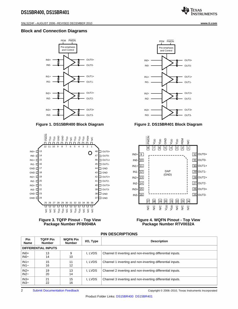
Block and Connection Diagrams
Figure 1. DS15BR400 Block Diagram Figure 2. DS15BR401 Block Diagram
Figure 3. TQFP Pinout - Top View Figure 4. WQFN Pinout - Top ViewPackage Number PFB0048A Package Number RTV0032A
PIN DESCRIPTIONSPin TQFP Pin WQFN Pin I/O, Type DescriptionName Number Number
DIFFERENTIAL INPUTS
IN0+ 13 9 I, LVDS Channel 0 inverting and non-inverting differential inputs.IN0− 14 10
IN1+ 15 11 I, LVDS Channel 1 inverting and non-inverting differential inputs.IN1− 16 12
IN2+ 19 13 I, LVDS Channel 2 inverting and non-inverting differential inputs.IN2− 20 14
IN3+ 21 15 I, LVDS Channel 3 inverting and non-inverting differential inputs.IN3− 22 16
2 Submit Documentation Feedback Copyright © 2006–2010, Texas Instruments Incorporated
Product Folder Links: DS15BR400 DS15BR401
DS15BR400, DS15BR401
www.ti.com SNLS224F –AUGUST 2006–REVISED DECEMBER 2010
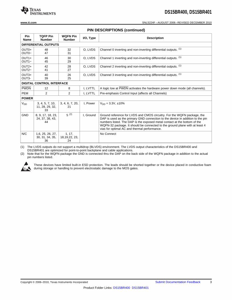
PIN DESCRIPTIONS (continued)
Pin TQFP Pin WQFN Pin I/O, Type DescriptionName Number Number
DIFFERENTIAL OUTPUTS
OUT0+ 48 32 O, LVDS Channel 0 inverting and non-inverting differential outputs. (1)
OUT0− 47 31
OUT1+ 46 30 O, LVDS Channel 1 inverting and non-inverting differential outputs. (1)
OUT1− 45 29
OUT2+ 42 28 O, LVDS Channel 2 inverting and non-inverting differential outputs. (1)
OUT2− 41 27
OUT3+ 40 26 O, LVDS Channel 3 inverting and non-inverting differential outputs. (1)
OUT3- 39 25
DIGITAL CONTROL INTERFACE
PWDN 12 8 I, LVTTL A logic low at PWDN activates the hardware power down mode (all channels).
PEM 2 2 I, LVTTL Pre-emphasis Control Input (affects all Channels)
POWER
VDD 3, 4, 5, 7, 10, 3, 4, 6, 7, 20, I, Power VDD = 3.3V, ±10%11, 28, 29, 32, 21
33
GND 8, 9, 17, 18, 23, 5 (2) I, Ground Ground reference for LVDS and CMOS circuitry. For the WQFN package, the24, 37, 38, 43, DAP is used as the primary GND connection to the device in addition to the pin
44 numbers listed. The DAP is the exposed metal contact at the bottom of theWQFN-32 package. It should be connected to the ground plane with at least 4vias for optimal AC and thermal performance.
N/C 1,6, 25, 26, 27, 1, 17, No Connect30, 31, 34, 35, 18,19,22, 23,
36 24
(1) The LVDS outputs do not support a multidrop (BLVDS) environment. The LVDS output characteristics of the DS15BR400 andDS15BR401 are optimized for point-to-point backplane and cable applications.
(2) Note that for the WQFN package the GND is connected thru the DAP on the back side of the WQFN package in addition to the actualpin numbers listed.
These devices have limited built-in ESD protection. The leads should be shorted together or the device placed in conductive foamduring storage or handling to prevent electrostatic damage to the MOS gates.
Copyright © 2006–2010, Texas Instruments Incorporated Submit Documentation Feedback 3
Product Folder Links: DS15BR400 DS15BR401
DS15BR400, DS15BR401
SNLS224F –AUGUST 2006–REVISED DECEMBER 2010 www.ti.com
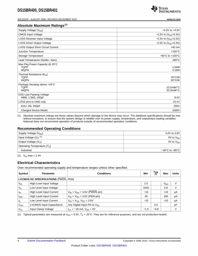
Absolute Maximum Ratings (1)
Supply Voltage (VDD) −0.3V to +4.0V
CMOS Input Voltage −0.3V to (VDD+0.3V)
LVDS Receiver Input Voltage −0.3V to (VDD+0.3V)
LVDS Driver Output Voltage −0.3V to (VDD+0.3V)
LVDS Output Short Circuit Current +40 mA
Junction Temperature +150°C
Storage Temperature −65°C to +150°C
Lead Temperature (Solder, 4sec) 260°C
Max Pkg Power Capacity @ 25°CTQFP 1.64WWQFN 4.16W
Thermal Resistance (θJA)TQFP 76°C/WWQFN 30°C/W
Package Derating above +25°CTQFP 13.2mW/°CWQFN 33.3mW/°C
ESD Last Passing VoltageHBM, 1.5kΩ, 100pF 8 kV
LVDS pins to GND only 15 kV
EIAJ, 0Ω, 200pF 250V
Charged Device Model 1000V
(1) Absolute maximum ratings are those values beyond which damage to the device may occur. The databook specifications should be met,without exception, to ensure that the system design is reliable over its power supply, temperature, and output/input loading variables.National does not recommend operation of products outside of recommended operation conditions.
Recommended Operating ConditionsSupply Voltage (VDD) 3.0V to 3.6V
Input Voltage (VI)(1) 0V to VDD
Output Voltage (VO) 0V to VDD
Operating Temperature (TA)
Industrial −40°C to +85°C
(1) VID max < 2.4V
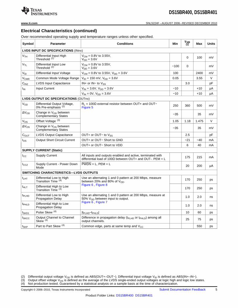
Electrical CharacteristicsOver recommended operating supply and temperature ranges unless other specified.
TypSymbol Parameter Conditions Min Max Units(1)
LVCMOS DC SPECIFICATIONS (PWDN, PEM)
VIH High Level Input Voltage 2.0 VDD V
VIL Low Level Input Voltage GND 0.8 V
IIH High Level Input Current VIN = VDD = 3.6V (PWDN pin) −10 +10 µA
IIHR High Level Input Current VIN = VDD = 3.6V (PEM pin) 40 200 µA
IIL Low Level Input Current VIN = VSS, VDD = 3.6V −10 +10 µA
CIN1 LVCMOS Input Capacitance Any Digital Input Pin to VSS 5.5 pF
VCL Input Clamp Voltage ICL = −18 mA, VDD = 0V −1.5 −0.8 V
(1) Typical parameters are measured at VDD = 3.3V, TA = 25°C. They are for reference purposes, and are not production-tested.
4 Submit Documentation Feedback Copyright © 2006–2010, Texas Instruments Incorporated
Product Folder Links: DS15BR400 DS15BR401
DS15BR400, DS15BR401
www.ti.com SNLS224F –AUGUST 2006–REVISED DECEMBER 2010
Electrical Characteristics (continued)Over recommended operating supply and temperature ranges unless other specified.
TypSymbol Parameter Conditions Min Max Units(1)
LVDS INPUT DC SPECIFICATIONS (INn±)
VTH Differential Input High VCM = 0.8V to 3.55V, 0 100 mVThreshold (2) VDD = 3.6V
VTL Differential Input Low VCM = 0.8V to 3.55V, −100 0 mVThreshold (2) VDD = 3.6V
VID Differential Input Voltage VCM = 0.8V to 3.55V, VDD = 3.6V 100 2400 mV
VCMR Common Mode Voltage Range VID = 150 mV, VDD = 3.6V 0.05 3.55 V
CIN2 LVDS Input Capacitance IN+ or IN− to VSS 3.0 pF
IIN Input Current VIN = 3.6V, VDD = 3.6V −10 +10 µA
VIN = 0V, VDD = 3.6V −10 +10 µA
LVDS OUTPUT DC SPECIFICATIONS (OUTn±)
VOD Differential Output Voltage, RL = 100Ω external resistor between OUT+ and OUT− 250 360 500 mV0% Pre-emphasis (2) Figure 5
ΔVOD Change in VOD between −35 35 mVComplementary States
VOS Offset Voltage (3) 1.05 1.18 1.475 V
ΔVOS Change in VOS between −35 35 mVComplementary States
COUT LVDS Output Capacitance OUT+ or OUT− to VSS 2.5 pF
IOS Output Short Circuit Current OUT+ or OUT− Short to GND −21 −40 mA
OUT+ or OUT− Short to VDD 6 40 mA
SUPPLY CURRENT (Static)
ICC Supply Current All inputs and outputs enabled and active, terminated with 175 215 mAdifferential load of 100Ω between OUT+ and OUT-. PEM = L
ICCZ Supply Current - Power Down PWDN = L, PEM = L 20 200 µAMode
SWITCHING CHARACTERISTICS—LVDS OUTPUTS
tLHT Differential Low to High Use an alternating 1 and 0 pattern at 200 Mbps, measure 170 250 psTransition Time (4) between 20% and 80% of VOD.Figure 6 , Figure 8tHLT Differential High to Low 170 250 psTransition Time (4)
tPLHD Differential Low to High Use an alternating 1 and 0 pattern at 200 Mbps, measure at 1.0 2.0 nsPropagation Delay 50% VOD between input to output.Figure 6 , Figure 7tPHLD Differential High to Low 1.0 2.0 nsPropagation Delay
tSKD1 Pulse Skew (4) |tPLHD–tPHLD| 10 60 ps
tSKCC Output Channel to Channel Difference in propagation delay (tPLHD or tPHLD) among all 25 75 psSkew (4) output channels.
tSKP Part to Part Skew (4) Common edge, parts at same temp and VCC 550 ps
(2) Differential output voltage VOD is defined as ABS(OUT+–OUT−). Differential input voltage VID is defined as ABS(IN+–IN−).(3) Output offset voltage VOS is defined as the average of the LVDS single-ended output voltages at logic high and logic low states.(4) Not production tested. Guaranteed by a statistical analysis on a sample basis at the time of characterization.
Copyright © 2006–2010, Texas Instruments Incorporated Submit Documentation Feedback 5
Product Folder Links: DS15BR400 DS15BR401
RL
OUT+
OUT-
IN+
IN-
Signal Generator
1/4 DS15BR400
R D
R D RL
VOH
VOL
OUT+
OUT-
IN+
IN-
Power Supply
Power Supply
1/4 DS15BR400
DS15BR400, DS15BR401
SNLS224F –AUGUST 2006–REVISED DECEMBER 2010 www.ti.com
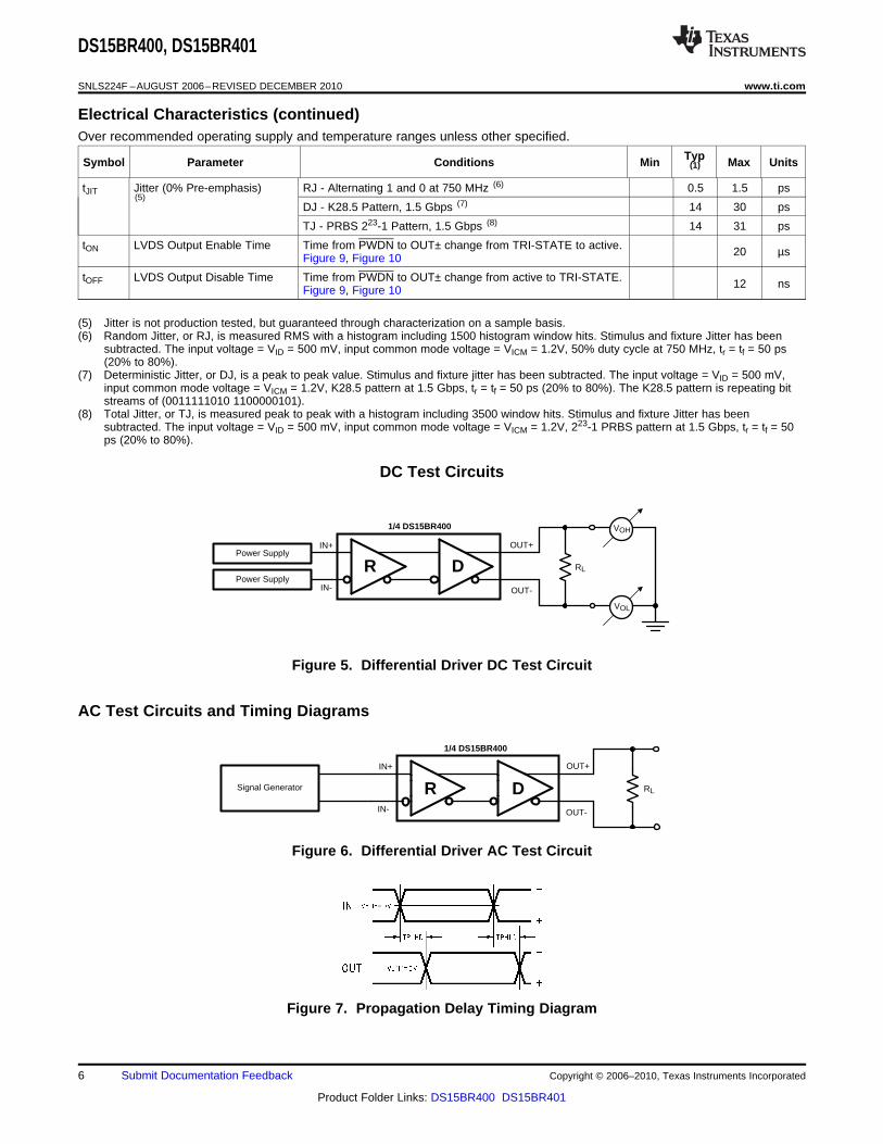
Electrical Characteristics (continued)Over recommended operating supply and temperature ranges unless other specified.
TypSymbol Parameter Conditions Min Max Units(1)
tJIT Jitter (0% Pre-emphasis) RJ - Alternating 1 and 0 at 750 MHz (6) 0.5 1.5 ps(5)
DJ - K28.5 Pattern, 1.5 Gbps (7) 14 30 ps
TJ - PRBS 223-1 Pattern, 1.5 Gbps (8) 14 31 ps
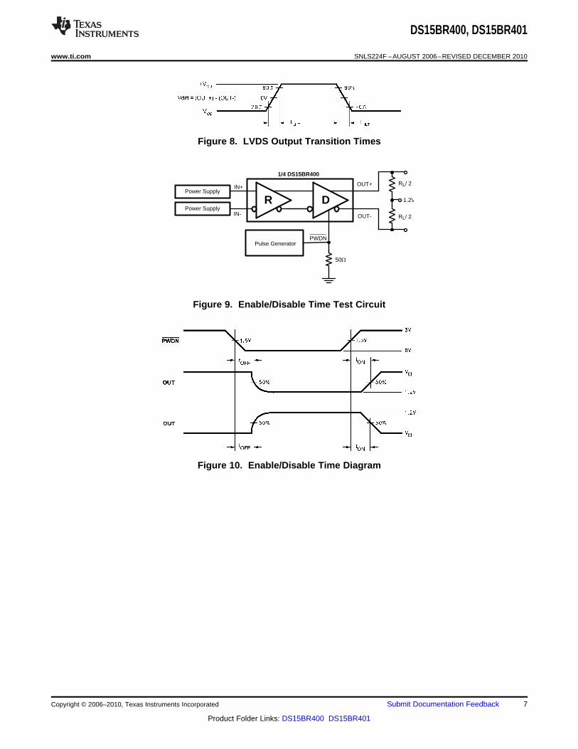
tON LVDS Output Enable Time Time from PWDN to OUT± change from TRI-STATE to active. 20 µsFigure 9, Figure 10
tOFF LVDS Output Disable Time Time from PWDN to OUT± change from active to TRI-STATE. 12 nsFigure 9, Figure 10
(5) Jitter is not production tested, but guaranteed through characterization on a sample basis.(6) Random Jitter, or RJ, is measured RMS with a histogram including 1500 histogram window hits. Stimulus and fixture Jitter has been
subtracted. The input voltage = VID = 500 mV, input common mode voltage = VICM = 1.2V, 50% duty cycle at 750 MHz, tr = tf = 50 ps(20% to 80%).
(7) Deterministic Jitter, or DJ, is a peak to peak value. Stimulus and fixture jitter has been subtracted. The input voltage = VID = 500 mV,input common mode voltage = VICM = 1.2V, K28.5 pattern at 1.5 Gbps, tr = tf = 50 ps (20% to 80%). The K28.5 pattern is repeating bitstreams of (0011111010 1100000101).
(8) Total Jitter, or TJ, is measured peak to peak with a histogram including 3500 window hits. Stimulus and fixture Jitter has beensubtracted. The input voltage = VID = 500 mV, input common mode voltage = VICM = 1.2V, 223-1 PRBS pattern at 1.5 Gbps, tr = tf = 50ps (20% to 80%).
DC Test Circuits
Figure 5. Differential Driver DC Test Circuit
AC Test Circuits and Timing Diagrams
Figure 6. Differential Driver AC Test Circuit
Figure 7. Propagation Delay Timing Diagram
6 Submit Documentation Feedback Copyright © 2006–2010, Texas Instruments Incorporated
Product Folder Links: DS15BR400 DS15BR401
R D
OUT+
OUT-
IN+
IN-Power Supply
50:
Pulse GeneratorPWDN
1/4 DS15BR400
RL/ 2
RL/ 2
1.2V
Power Supply
DS15BR400, DS15BR401
www.ti.com SNLS224F –AUGUST 2006–REVISED DECEMBER 2010
Figure 8. LVDS Output Transition Times
Figure 9. Enable/Disable Time Test Circuit
Figure 10. Enable/Disable Time Diagram
Copyright © 2006–2010, Texas Instruments Incorporated Submit Documentation Feedback 7
Product Folder Links: DS15BR400 DS15BR401
DS15BR400, DS15BR401
SNLS224F –AUGUST 2006–REVISED DECEMBER 2010 www.ti.com
APPLICATION INFORMATION
INTERNAL TERMINATIONS
The DS15BR400 has integrated termination resistors on both the input and outputs. The inputs have a 100Ωresistor across the differential pair, placing the receiver termination as close as possible to the input stage of thedevice. The LVDS outputs also contain an integrated 100Ω ohm termination resistor, this resistor is used tominimize the output return loss and does not take the place of the 100 ohm termination at the inputs to thereceiving device. The integrated terminations improve signal integrity and decrease the external componentcount resulting in space savings. The DS15BR401 has 100Ω output terminations only.
OUTPUT CHARACTERISTICS
The output characteristics of the DS15BRB400/DS15BR401 have been optimized for point-to-point backplaneand cable applications, and are not intended for multipoint or multidrop signaling.
POWERDOWN MODE
The PWDN input activates a hardware powerdown mode. When the powerdown mode is active (PWDN=L), allinput and output buffers and internal bias circuitry are powered off. When exiting powerdown mode, there is adelay associated with turning on bandgap references and input/output buffer circuits as indicated in the LVDSOutput Switching Characteristics
Upon asserting the power down function (PWDN = Low), and if the Pre-emphasis feature is enable, it is possiblefor the driver output to source current for a short amount of time lifting the output common mode to VDD. Toprevent this occurrence, a load discharge pull down path can be used on either output (1 kΩ to groundrecommended). Alternately, a commonly deployed external failsafe network will also provide this path (seeINPUT FAILSAFE BIASING). The occurrence of this is application dependant, and parameters that will effect ifthis is of concern include: AC coupling, use of the powerdown feature, presence of the discharge path, presenceof the failsafe biasing, the usage of the pre-emphasis feature, and input characteristics of the downstream LVDSReceiver.
PRE-EMPHASIS
Pre-emphasis dramatically reduces ISI jitter from long or lossy transmission media. One pin is used to select thepre-emphasis level for all outputs, off or on. The pre-emphasis boost is approximately 6 dB at 750 MHz.
Table 1. Pre-emphasis Control Selection Table
PEM Pre-Emphasis
0 Off
1 On
INPUT FAILSAFE BIASING
Failsafe biasing of the LVDS link should be considered if the downstream Receiver is ON and enabled when thesource is in TRI-STATE, powered off, or removed. This will set a valid known input state to the active receiver.This is accomplished by using a pull up resistor to VDD on the ‘plus’ line, and a pull down resistor to GND on the‘minus’ line. Resistor values are in the 750 Ohm to several kΩ range. The exact value depends upon the desiredcommon mode bias point, termination resistor(s) and desired input differential voltage setting. Please refer toapplication note AN-1194 “Failsafe Biasing of LVDS interfaces” for more information and a general discussion.
DECOUPLING
Each power or ground lead of the DS15BR400 should be connected to the PCB through a low inductance path.For best results, one or more vias are used to connect a power or ground pin to the nearby plane. Ideally, viaplacement is immediately adjacent to the pin to avoid adding trace inductance. Placing power plane closer to thetop of the board reduces effective via length and its associated inductance.
8 Submit Documentation Feedback Copyright © 2006–2010, Texas Instruments Incorporated
Product Folder Links: DS15BR400 DS15BR401
OUT+
OUT-
150-250:
100: Differential T-Line
LVDS Receiver
IN+
IN-
100:
LVPECL Driver
150-250:
OUT+
OUT-
50:50:
VCC
CML3.3V or CML2.5V Driver
100: Differential T-Line
DS15BR400 Receiver
IN+
IN-
100:
OUT+
OUT-
DS15BR400 Receiver
IN+
IN-
100: Differential T-Line
100:
LVDS Driver
DS15BR400, DS15BR401
www.ti.com SNLS224F –AUGUST 2006–REVISED DECEMBER 2010
Bypass capacitors should be placed close to VDD pins. Small physical size capacitors, such as 0402, X7R,surface mount capacitors should be used to minimize body inductance of capacitors. Each bypass capacitor isconnected to the power and ground plane through vias tangent to the pads of the capacitor. An X7R surfacemount capacitor of size 0402 has about 0.5 nH of body inductance. At frequencies above 30 MHz or so, X7Rcapacitors behave as low impedance inductors. To extend the operating frequency range to a few hundred MHz,an array of different capacitor values like 100 pF, 1 nF, 0.03 µF, and 0.1 µF are commonly used in parallel. Themost effective bypass capacitor can be built using sandwiched layers of power and ground at a separation of 2–3mils. With a 2 mil FR4 dielectric, there is approximately 500 pF per square inch of PCB.
The center dap of the WQFN package housing the DS15BR400 should be connected to a ground plane throughan array of vias. The via array reduces the effective inductance to ground and enhances the thermalperformance of the WQFN package.
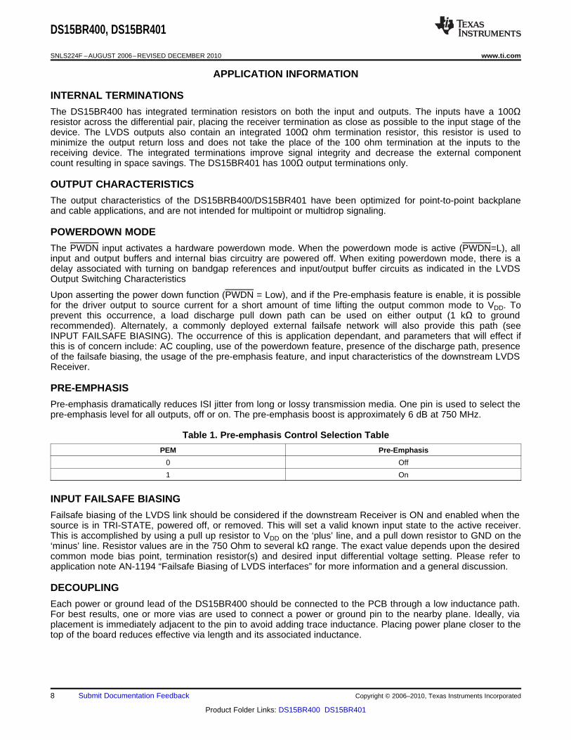
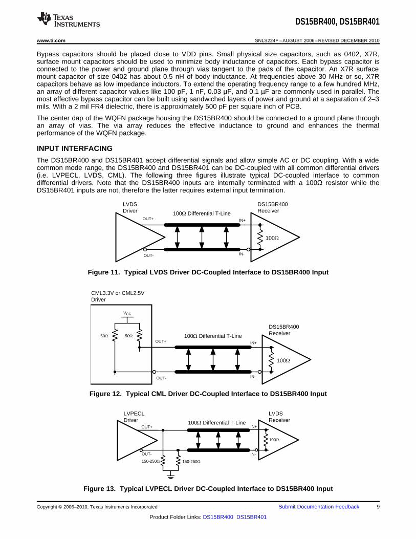
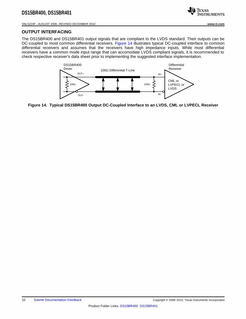
INPUT INTERFACING
The DS15BR400 and DS15BR401 accept differential signals and allow simple AC or DC coupling. With a widecommon mode range, the DS15BR400 and DS15BR401 can be DC-coupled with all common differential drivers(i.e. LVPECL, LVDS, CML). The following three figures illustrate typical DC-coupled interface to commondifferential drivers. Note that the DS15BR400 inputs are internally terminated with a 100Ω resistor while theDS15BR401 inputs are not, therefore the latter requires external input termination.
Figure 11. Typical LVDS Driver DC-Coupled Interface to DS15BR400 Input
Figure 12. Typical CML Driver DC-Coupled Interface to DS15BR400 Input
Figure 13. Typical LVPECL Driver DC-Coupled Interface to DS15BR400 Input
Copyright © 2006–2010, Texas Instruments Incorporated Submit Documentation Feedback 9
Product Folder Links: DS15BR400 DS15BR401
OUT+
OUT-
CML or LVPECL or LVDS
IN+
IN-
100:
100: Differential T-Line
Differential Receiver
DS15BR400 Driver
100:
DS15BR400, DS15BR401
SNLS224F –AUGUST 2006–REVISED DECEMBER 2010 www.ti.com
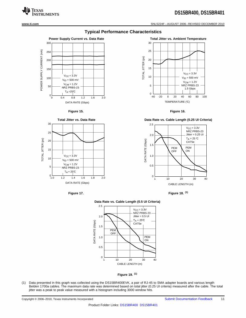
OUTPUT INTERFACING
The DS15BR400 and DS15BR401 output signals that are compliant to the LVDS standard. Their outputs can beDC-coupled to most common differential receivers. Figure 14 illustrates typical DC-coupled interface to commondifferential receivers and assumes that the receivers have high impedance inputs. While most differentialreceivers have a common mode input range that can accomodate LVDS compliant signals, it is recommended tocheck respective receiver's data sheet prior to implementing the suggested interface implementation.
Figure 14. Typical DS15BR400 Output DC-Coupled Interface to an LVDS, CML or LVPECL Receiver
10 Submit Documentation Feedback Copyright © 2006–2010, Texas Instruments Incorporated
Product Folder Links: DS15BR400 DS15BR401
1 10 20 30 40
0.5
1.0
1.5
2.0
2.5
CABLE LENGTH (m)
DA
TA
RA
TE
(G
bps)
VCC = 3.3VNRZ PRBS-23Jitter = 0.5 UI
TA = 25°CCAT5e
PEMON
PEM OFF
0
1 10 20 30 40
0.5
1.0
1.5
2.0
2.5
CABLE LENGTH (m)
DA
TA
RA
TE
(G
bps)
VCC = 3.3VNRZ PRBS-23Jitter = 0.25 UI
TA = 25 °CCAT5e
PEMON
PEM OFF
0
30
25
20
15
10
5
01.0 1.2 1.4 1.6 1.8 2.0
VCC = 3.3V
VID = 500 mV
VCM = 1.2VNRZ PRBS-23
TA = 25°C
TO
TA
L JI
TT
ER
(ps
)
DATA RATE (Gbps)
300
250
200
150
100
50
00 0.4 0.8 1.2 1.6 2.0
VCC = 3.3V
VID = 500 mV
VCM = 1.2VNRZ PRBS-23
TA =25°C
PO
WE
R S
UP
PLY
CU
RR
EN
T (
mA
)
DATA RATE (Gbps)
25
20
30
15
10
5
0-40 -20 0 20 40 60 80 100
VCC = 3.3V
VID = 500 mV
VCM = 1.2VNRZ PRBS-23
1.5 Gbps
TEMPERATURE (°C)
TO
TA
L JI
TT
ER
(ps
)
DS15BR400, DS15BR401
www.ti.com SNLS224F –AUGUST 2006–REVISED DECEMBER 2010
Typical Performance Characteristics
Power Supply Current vs. Data Rate Total Jitter vs. Ambient Temperature
Figure 15. Figure 16.
Total Jitter vs. Data Rate Data Rate vs. Cable Length (0.25 UI Criteria)
Figure 17. Figure 18. (1)
Data Rate vs. Cable Length (0.5 UI Criteria)
Figure 19. (1)
(1) Data presented in this graph was collected using the DS15BR400EVK, a pair of RJ-45 to SMA adapter boards and various lengthBelden 1700a cables. The maximum data rate was determined based on total jitter (0.25 UI criteria) measured after the cable. The totaljitter was a peak to peak value measured with a histogram including 3000 window hits.
Copyright © 2006–2010, Texas Instruments Incorporated Submit Documentation Feedback 11
Product Folder Links: DS15BR400 DS15BR401
PACKAGE OPTION ADDENDUM
www.ti.com 9-Mar-2013
Addendum-Page 1
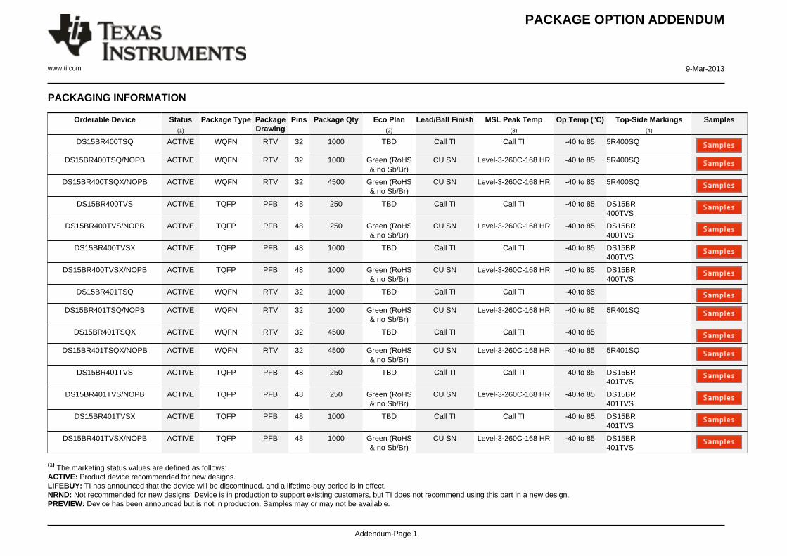
PACKAGING INFORMATION
Orderable Device Status(1)
Package Type PackageDrawing
Pins Package Qty Eco Plan(2)
Lead/Ball Finish MSL Peak Temp(3)
Op Temp (°C) Top-Side Markings(4)
Samples
DS15BR400TSQ ACTIVE WQFN RTV 32 1000 TBD Call TI Call TI -40 to 85 5R400SQ
DS15BR400TSQ/NOPB ACTIVE WQFN RTV 32 1000 Green (RoHS& no Sb/Br)
CU SN Level-3-260C-168 HR -40 to 85 5R400SQ
DS15BR400TSQX/NOPB ACTIVE WQFN RTV 32 4500 Green (RoHS& no Sb/Br)
CU SN Level-3-260C-168 HR -40 to 85 5R400SQ
DS15BR400TVS ACTIVE TQFP PFB 48 250 TBD Call TI Call TI -40 to 85 DS15BR400TVS
DS15BR400TVS/NOPB ACTIVE TQFP PFB 48 250 Green (RoHS& no Sb/Br)
CU SN Level-3-260C-168 HR -40 to 85 DS15BR400TVS
DS15BR400TVSX ACTIVE TQFP PFB 48 1000 TBD Call TI Call TI -40 to 85 DS15BR400TVS
DS15BR400TVSX/NOPB ACTIVE TQFP PFB 48 1000 Green (RoHS& no Sb/Br)
CU SN Level-3-260C-168 HR -40 to 85 DS15BR400TVS
DS15BR401TSQ ACTIVE WQFN RTV 32 1000 TBD Call TI Call TI -40 to 85
DS15BR401TSQ/NOPB ACTIVE WQFN RTV 32 1000 Green (RoHS& no Sb/Br)
CU SN Level-3-260C-168 HR -40 to 85 5R401SQ
DS15BR401TSQX ACTIVE WQFN RTV 32 4500 TBD Call TI Call TI -40 to 85
DS15BR401TSQX/NOPB ACTIVE WQFN RTV 32 4500 Green (RoHS& no Sb/Br)
CU SN Level-3-260C-168 HR -40 to 85 5R401SQ
DS15BR401TVS ACTIVE TQFP PFB 48 250 TBD Call TI Call TI -40 to 85 DS15BR401TVS
DS15BR401TVS/NOPB ACTIVE TQFP PFB 48 250 Green (RoHS& no Sb/Br)
CU SN Level-3-260C-168 HR -40 to 85 DS15BR401TVS
DS15BR401TVSX ACTIVE TQFP PFB 48 1000 TBD Call TI Call TI -40 to 85 DS15BR401TVS
DS15BR401TVSX/NOPB ACTIVE TQFP PFB 48 1000 Green (RoHS& no Sb/Br)
CU SN Level-3-260C-168 HR -40 to 85 DS15BR401TVS
(1) The marketing status values are defined as follows:ACTIVE: Product device recommended for new designs.LIFEBUY: TI has announced that the device will be discontinued, and a lifetime-buy period is in effect.NRND: Not recommended for new designs. Device is in production to support existing customers, but TI does not recommend using this part in a new design.PREVIEW: Device has been announced but is not in production. Samples may or may not be available.
PACKAGE OPTION ADDENDUM
www.ti.com 9-Mar-2013
Addendum-Page 2
OBSOLETE: TI has discontinued the production of the device.
(2) Eco Plan - The planned eco-friendly classification: Pb-Free (RoHS), Pb-Free (RoHS Exempt), or Green (RoHS & no Sb/Br) - please check http://www.ti.com/productcontent for the latest availabilityinformation and additional product content details.TBD: The Pb-Free/Green conversion plan has not been defined.Pb-Free (RoHS): TI's terms "Lead-Free" or "Pb-Free" mean semiconductor products that are compatible with the current RoHS requirements for all 6 substances, including the requirement thatlead not exceed 0.1% by weight in homogeneous materials. Where designed to be soldered at high temperatures, TI Pb-Free products are suitable for use in specified lead-free processes.Pb-Free (RoHS Exempt): This component has a RoHS exemption for either 1) lead-based flip-chip solder bumps used between the die and package, or 2) lead-based die adhesive used betweenthe die and leadframe. The component is otherwise considered Pb-Free (RoHS compatible) as defined above.Green (RoHS & no Sb/Br): TI defines "Green" to mean Pb-Free (RoHS compatible), and free of Bromine (Br) and Antimony (Sb) based flame retardants (Br or Sb do not exceed 0.1% by weightin homogeneous material)
(3) MSL, Peak Temp. -- The Moisture Sensitivity Level rating according to the JEDEC industry standard classifications, and peak solder temperature.
(4) Only one of markings shown within the brackets will appear on the physical device.
Important Information and Disclaimer:The information provided on this page represents TI's knowledge and belief as of the date that it is provided. TI bases its knowledge and belief on informationprovided by third parties, and makes no representation or warranty as to the accuracy of such information. Efforts are underway to better integrate information from third parties. TI has taken andcontinues to take reasonable steps to provide representative and accurate information but may not have conducted destructive testing or chemical analysis on incoming materials and chemicals.TI and TI suppliers consider certain information to be proprietary, and thus CAS numbers and other limited information may not be available for release.
In no event shall TI's liability arising out of such information exceed the total purchase price of the TI part(s) at issue in this document sold by TI to Customer on an annual basis.
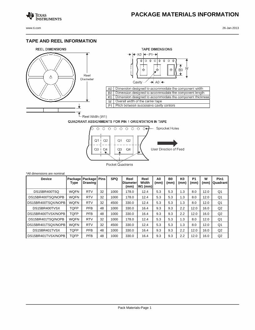
TAPE AND REEL INFORMATION
*All dimensions are nominal
Device PackageType
PackageDrawing
Pins SPQ ReelDiameter
(mm)
ReelWidth
W1 (mm)
A0(mm)
B0(mm)
K0(mm)
P1(mm)
W(mm)
Pin1Quadrant
DS15BR400TSQ WQFN RTV 32 1000 178.0 12.4 5.3 5.3 1.3 8.0 12.0 Q1
DS15BR400TSQ/NOPB WQFN RTV 32 1000 178.0 12.4 5.3 5.3 1.3 8.0 12.0 Q1
DS15BR400TSQX/NOPB WQFN RTV 32 4500 330.0 12.4 5.3 5.3 1.3 8.0 12.0 Q1
DS15BR400TVSX TQFP PFB 48 1000 330.0 16.4 9.3 9.3 2.2 12.0 16.0 Q2
DS15BR400TVSX/NOPB TQFP PFB 48 1000 330.0 16.4 9.3 9.3 2.2 12.0 16.0 Q2
DS15BR401TSQ/NOPB WQFN RTV 32 1000 178.0 12.4 5.3 5.3 1.3 8.0 12.0 Q1
DS15BR401TSQX/NOPB WQFN RTV 32 4500 330.0 12.4 5.3 5.3 1.3 8.0 12.0 Q1
DS15BR401TVSX TQFP PFB 48 1000 330.0 16.4 9.3 9.3 2.2 12.0 16.0 Q2
DS15BR401TVSX/NOPB TQFP PFB 48 1000 330.0 16.4 9.3 9.3 2.2 12.0 16.0 Q2
PACKAGE MATERIALS INFORMATION
www.ti.com 26-Jan-2013
Pack Materials-Page 1
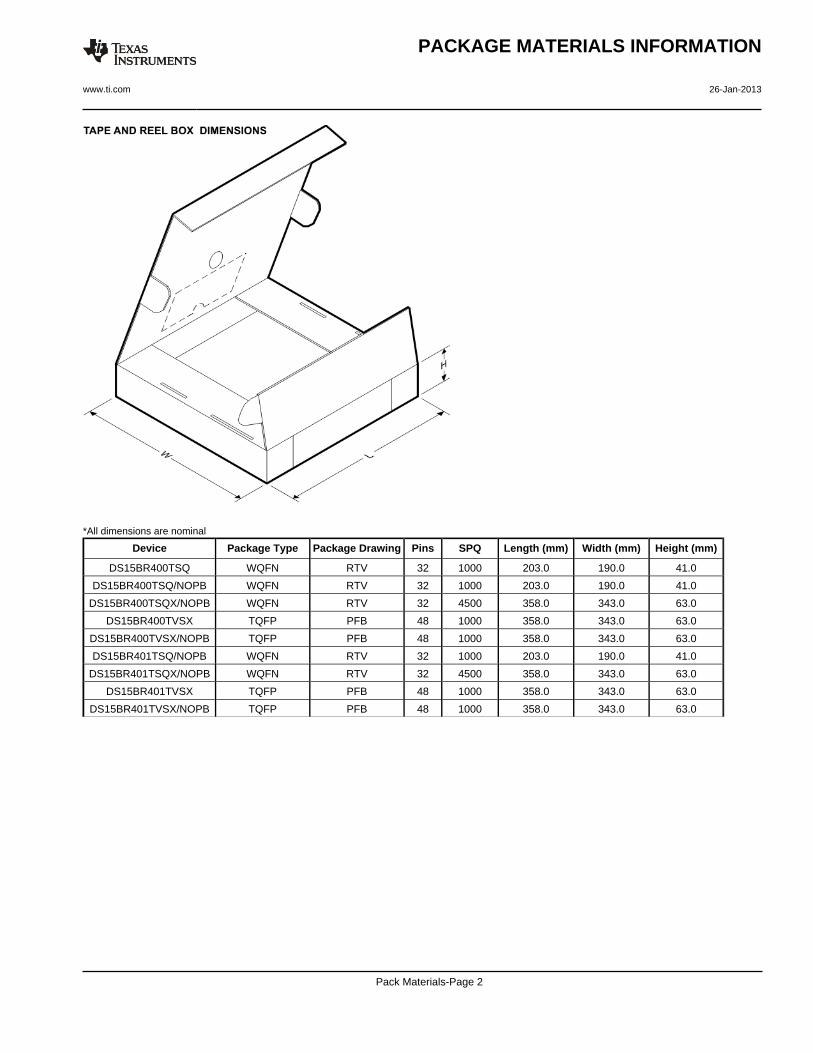
*All dimensions are nominal
Device Package Type Package Drawing Pins SPQ Length (mm) Width (mm) Height (mm)
DS15BR400TSQ WQFN RTV 32 1000 203.0 190.0 41.0
DS15BR400TSQ/NOPB WQFN RTV 32 1000 203.0 190.0 41.0
DS15BR400TSQX/NOPB WQFN RTV 32 4500 358.0 343.0 63.0
DS15BR400TVSX TQFP PFB 48 1000 358.0 343.0 63.0
DS15BR400TVSX/NOPB TQFP PFB 48 1000 358.0 343.0 63.0
DS15BR401TSQ/NOPB WQFN RTV 32 1000 203.0 190.0 41.0
DS15BR401TSQX/NOPB WQFN RTV 32 4500 358.0 343.0 63.0
DS15BR401TVSX TQFP PFB 48 1000 358.0 343.0 63.0
DS15BR401TVSX/NOPB TQFP PFB 48 1000 358.0 343.0 63.0
PACKAGE MATERIALS INFORMATION
www.ti.com 26-Jan-2013
Pack Materials-Page 2
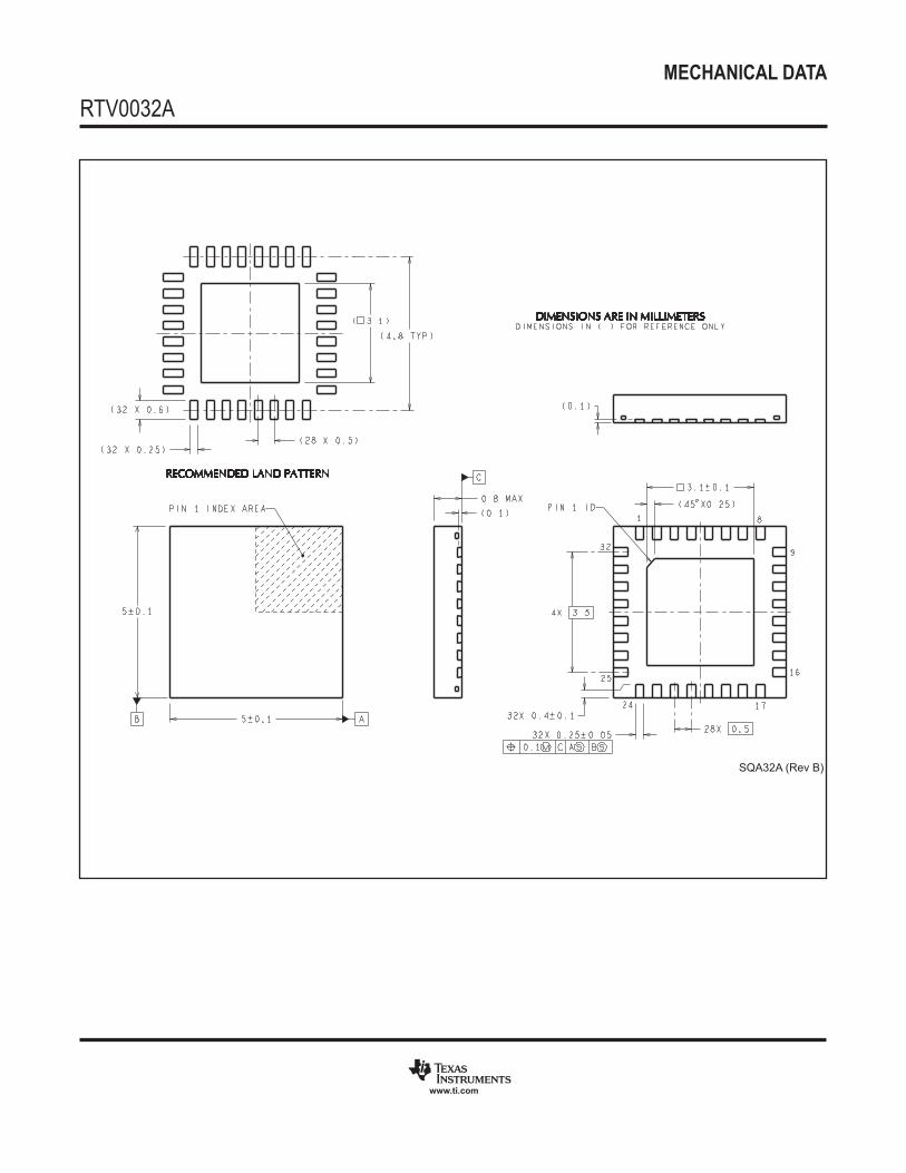
MECHANICAL DATA
RTV0032A
www.ti.com
SQA32A (Rev B)
MECHANICAL DATA
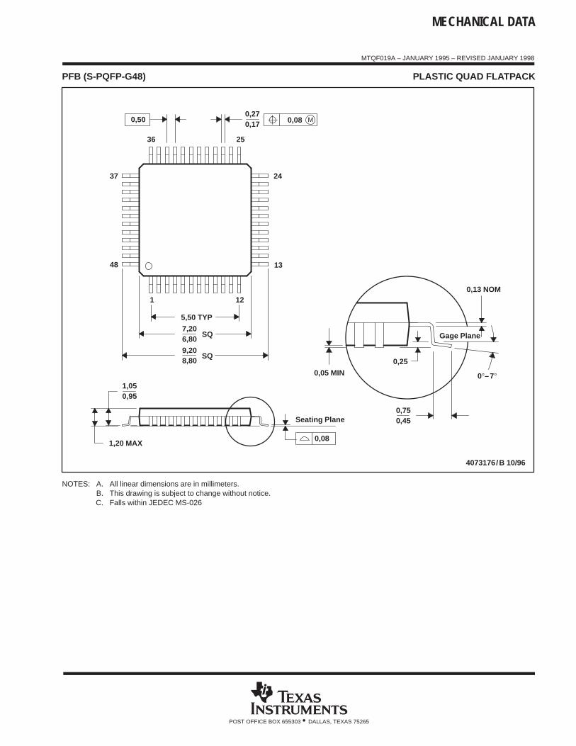
MTQF019A – JANUARY 1995 – REVISED JANUARY 1998
POST OFFICE BOX 655303 • DALLAS, TEXAS 75265
PFB (S-PQFP-G48) PLASTIC QUAD FLATPACK
4073176/B 10/96
Gage Plane
0,13 NOM
0,25
0,450,75
Seating Plane
0,05 MIN
0,170,27
24
25
13
12
SQ
36
37
7,206,80
48
1
5,50 TYP
SQ8,809,20
1,050,95
1,20 MAX0,08
0,50 M0,08
0°–7°
NOTES: A. All linear dimensions are in millimeters.B. This drawing is subject to change without notice.C. Falls within JEDEC MS-026
IMPORTANT NOTICE
Texas Instruments Incorporated and its subsidiaries (TI) reserve the right to make corrections, enhancements, improvements and otherchanges to its semiconductor products and services per JESD46, latest issue, and to discontinue any product or service per JESD48, latestissue. Buyers should obtain the latest relevant information before placing orders and should verify that such information is current andcomplete. All semiconductor products (also referred to herein as “components”) are sold subject to TI’s terms and conditions of salesupplied at the time of order acknowledgment.
TI warrants performance of its components to the specifications applicable at the time of sale, in accordance with the warranty in TI’s termsand conditions of sale of semiconductor products. Testing and other quality control techniques are used to the extent TI deems necessaryto support this warranty. Except where mandated by applicable law, testing of all parameters of each component is not necessarilyperformed.
TI assumes no liability for applications assistance or the design of Buyers’ products. Buyers are responsible for their products andapplications using TI components. To minimize the risks associated with Buyers’ products and applications, Buyers should provideadequate design and operating safeguards.
TI does not warrant or represent that any license, either express or implied, is granted under any patent right, copyright, mask work right, orother intellectual property right relating to any combination, machine, or process in which TI components or services are used. Informationpublished by TI regarding third-party products or services does not constitute a license to use such products or services or a warranty orendorsement thereof. Use of such information may require a license from a third party under the patents or other intellectual property of thethird party, or a license from TI under the patents or other intellectual property of TI.
Reproduction of significant portions of TI information in TI data books or data sheets is permissible only if reproduction is without alterationand is accompanied by all associated warranties, conditions, limitations, and notices. TI is not responsible or liable for such altereddocumentation. Information of third parties may be subject to additional restrictions.
Resale of TI components or services with statements different from or beyond the parameters stated by TI for that component or servicevoids all express and any implied warranties for the associated TI component or service and is an unfair and deceptive business practice.TI is not responsible or liable for any such statements.
Buyer acknowledges and agrees that it is solely responsible for compliance with all legal, regulatory and safety-related requirementsconcerning its products, and any use of TI components in its applications, notwithstanding any applications-related information or supportthat may be provided by TI. Buyer represents and agrees that it has all the necessary expertise to create and implement safeguards whichanticipate dangerous consequences of failures, monitor failures and their consequences, lessen the likelihood of failures that might causeharm and take appropriate remedial actions. Buyer will fully indemnify TI and its representatives against any damages arising out of the useof any TI components in safety-critical applications.
In some cases, TI components may be promoted specifically to facilitate safety-related applications. With such components, TI’s goal is tohelp enable customers to design and create their own end-product solutions that meet applicable functional safety standards andrequirements. Nonetheless, such components are subject to these terms.
No TI components are authorized for use in FDA Class III (or similar life-critical medical equipment) unless authorized officers of the partieshave executed a special agreement specifically governing such use.
Only those TI components which TI has specifically designated as military grade or “enhanced plastic” are designed and intended for use inmilitary/aerospace applications or environments. Buyer acknowledges and agrees that any military or aerospace use of TI componentswhich have not been so designated is solely at the Buyer's risk, and that Buyer is solely responsible for compliance with all legal andregulatory requirements in connection with such use.
TI has specifically designated certain components as meeting ISO/TS16949 requirements, mainly for automotive use. In any case of use ofnon-designated products, TI will not be responsible for any failure to meet ISO/TS16949.
Products Applications
Audio www.ti.com/audio Automotive and Transportation www.ti.com/automotive
Amplifiers amplifier.ti.com Communications and Telecom www.ti.com/communications
Data Converters dataconverter.ti.com Computers and Peripherals www.ti.com/computers
DLP® Products www.dlp.com Consumer Electronics www.ti.com/consumer-apps
DSP dsp.ti.com Energy and Lighting www.ti.com/energy
Clocks and Timers www.ti.com/clocks Industrial www.ti.com/industrial
Interface interface.ti.com Medical www.ti.com/medical
Logic logic.ti.com Security www.ti.com/security
Power Mgmt power.ti.com Space, Avionics and Defense www.ti.com/space-avionics-defense
Microcontrollers microcontroller.ti.com Video and Imaging www.ti.com/video
RFID www.ti-rfid.com
OMAP Applications Processors www.ti.com/omap TI E2E Community e2e.ti.com
Wireless Connectivity www.ti.com/wirelessconnectivity
Mailing Address: Texas Instruments, Post Office Box 655303, Dallas, Texas 75265Copyright © 2013, Texas Instruments Incorporated
Mouser Electronics
Authorized Distributor
Click to View Pricing, Inventory, Delivery & Lifecycle Information: National Semiconductor (TI):
DS15BR400EVK/NOPB
Texas Instruments:
DS15BR400TSQ DS15BR400TSQ/NOPB DS15BR400TSQX DS15BR400TSQX/NOPB DS15BR400TVS
DS15BR400TVS/NOPB DS15BR400TVSX DS15BR400TVSX/NOPB DS15BR401TSQ DS15BR401TSQ/NOPB
DS15BR401TSQX DS15BR401TSQX/NOPB DS15BR401TVS DS15BR401TVS/NOPB DS15BR401TVSX
DS15BR401TVSX/NOPB