Development of a Radiation Hard CMOS Monolithic Pixel...
14
M. Battaglia 1,2 , D. Bisello 3 , D. Contarato 2 , P. Denes 2 , D. Doering 2 , P. Giubilato 2,3 , T.S. Kim 2 , Z. Lee 2 , S. Mattiazzo 3 , V. Radmilovic 2 1 University of California at Berkeley, Berkeley, CA, USA 2 Lawrence Berkeley National Laboratory, Berkeley, CA, USA 3 University of Padova & INFN Padova, Padova, IT, EU Development of a Radiation Hard CMOS Monolithic Pixel Sensor
Transcript of Development of a Radiation Hard CMOS Monolithic Pixel...
M. Battaglia1,2, D. Bisello3, D. Contarato2, P. Denes2, D. Doering2,P. Giubilato2,3, T.S. Kim2, Z. Lee2, S. Mattiazzo3, V. Radmilovic2
1University of California at Berkeley, Berkeley, CA, USA2Lawrence Berkeley National Laboratory, Berkeley, CA, USA
3University of Padova & INFN Padova, Padova, IT, EU
Development of a Radiation HardCMOS Monolithic Pixel Sensor
2/14KEK 2009 - Piero Giubilato – Development of a Radiation Hard CMOS MAPS
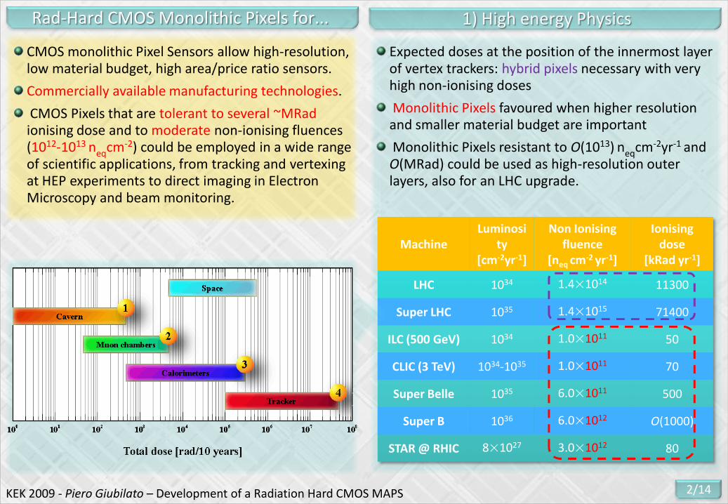
Expected doses at the position of the innermost layer of vertex trackers: hybrid pixels necessary with very high non-ionising doses
Monolithic Pixels favoured when higher resolution and smaller material budget are important
Monolithic Pixels resistant to O(1013) neqcm-2yr-1 and O(MRad) could be used as high-resolution outer layers, also for an LHC upgrade.
CMOS monolithic Pixel Sensors allow high-resolution, low material budget, high area/price ratio sensors.
Commercially available manufacturing technologies.
CMOS Pixels that are tolerant to several ~MRadionising dose and to moderate non-ionising fluences(1012-1013 neqcm-2) could be employed in a wide range of scientific applications, from tracking and vertexingat HEP experiments to direct imaging in Electron Microscopy and beam monitoring.
Rad-Hard CMOS Monolithic Pixels for... 1) High energy Physics
MachineLuminosi
ty[cm-2yr-1]
Non Ionising fluence
[neq cm-2 yr-1]
Ionising dose
[kRad yr-1]
LHC 1034 1.4×10¹⁴ 11300
Super LHC 1035 1.4×10¹⁵ 71400
ILC (500 GeV) 1034 1.0×10¹¹ 50
CLIC (3 TeV) 1034-1035 1.0×10¹¹ 70
Super Belle 1035 6.0×10¹¹ 500
Super B 1036 6.0×10¹² O(1000)
STAR @ RHIC 8×1027 3.0×10¹² 80
3/14KEK 2009 - Piero Giubilato – Development of a Radiation Hard CMOS MAPS
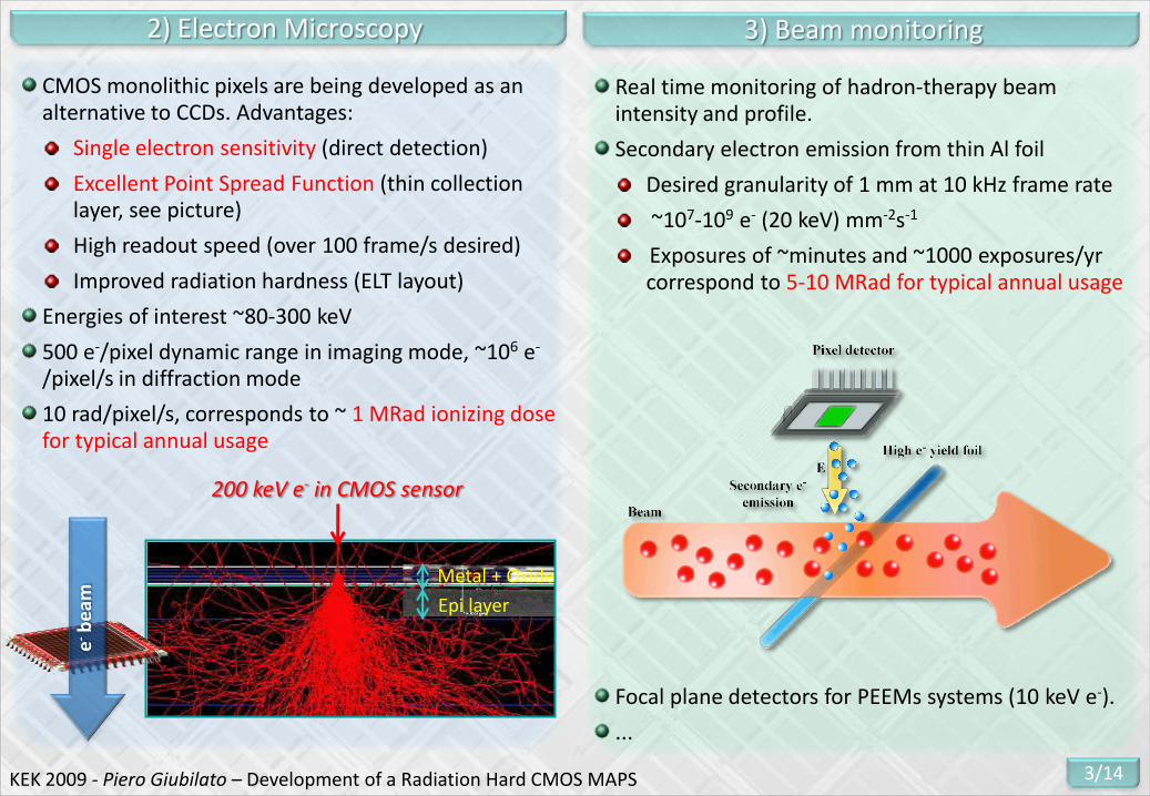
CMOS monolithic pixels are being developed as an alternative to CCDs. Advantages:
Single electron sensitivity (direct detection)
Excellent Point Spread Function (thin collection layer, see picture)
High readout speed (over 100 frame/s desired)
Improved radiation hardness (ELT layout)
Energies of interest ~80-300 keV
500 e-/pixel dynamic range in imaging mode, ~106 e-
/pixel/s in diffraction mode
10 rad/pixel/s, corresponds to ~ 1 MRad ionizing dose for typical annual usage
Real time monitoring of hadron-therapy beam intensity and profile.
Secondary electron emission from thin Al foil
Desired granularity of 1 mm at 10 kHz frame rate
~107-109 e- (20 keV) mm-2s-1
Exposures of ~minutes and ~1000 exposures/yr correspond to 5-10 MRad for typical annual usage
200 keV e- in CMOS sensor
Metal + Oxide
Epi layer
2) Electron Microscopy 3) Beam monitoring
e-b
eam
Focal plane detectors for PEEMs systems (10 keV e-).
...
4/14KEK 2009 - Piero Giubilato – Development of a Radiation Hard CMOS MAPS
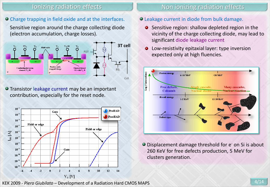
Charge trapping in field oxide and at the interfaces.
Sensitive region around the charge collecting diode (electron accumulation, charge losses).
Ionizing radiation effects Non ionizing radiation effects
Leakage current in diode from bulk damage.
Sensitive region: shallow depleted region in the vicinity of the charge collecting diode, may lead to significant diode leakage current
Low-resistivity epitaxial layer: type inversion expected only at high fluencies.
Transistor leakage current may be an important contribution, especially for the reset node.
Displacement damage threshold for e- on Si is about 260 KeV for free defects production, 5 MeV for clusters generation.
3T cell
5/14KEK 2009 - Piero Giubilato – Development of a Radiation Hard CMOS MAPS
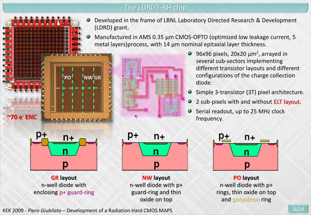
Developed in the frame of LBNL Laboratory Directed Research & Development (LDRD) grant.
Manufactured in AMS 0.35 μm CMOS-OPTO (optimized low leakage current, 5 metal layers)process, with 14 μm nominal epitaxial layer thickness.
96x96 pixels, 20x20 μm2, arrayed in several sub-sectors implementing different transistor layouts and different configurations of the charge collection diode.
Simple 3-transistor (3T) pixel architecture.
2 sub-pixels with and without ELT layout.
Serial readout, up to 25 MHz clock frequency.
GR layoutn-well diode with
enclosing p+ guard-ring
NW layoutn-well diode with p+ guard-ring and thin
oxide on top
PO layoutn-well diode with p+
rings, thin oxide on top and polysilicon ring
The LDRD2-RH chip
GRNWPO
~70 e- ENC
6/14KEK 2009 - Piero Giubilato – Development of a Radiation Hard CMOS MAPS
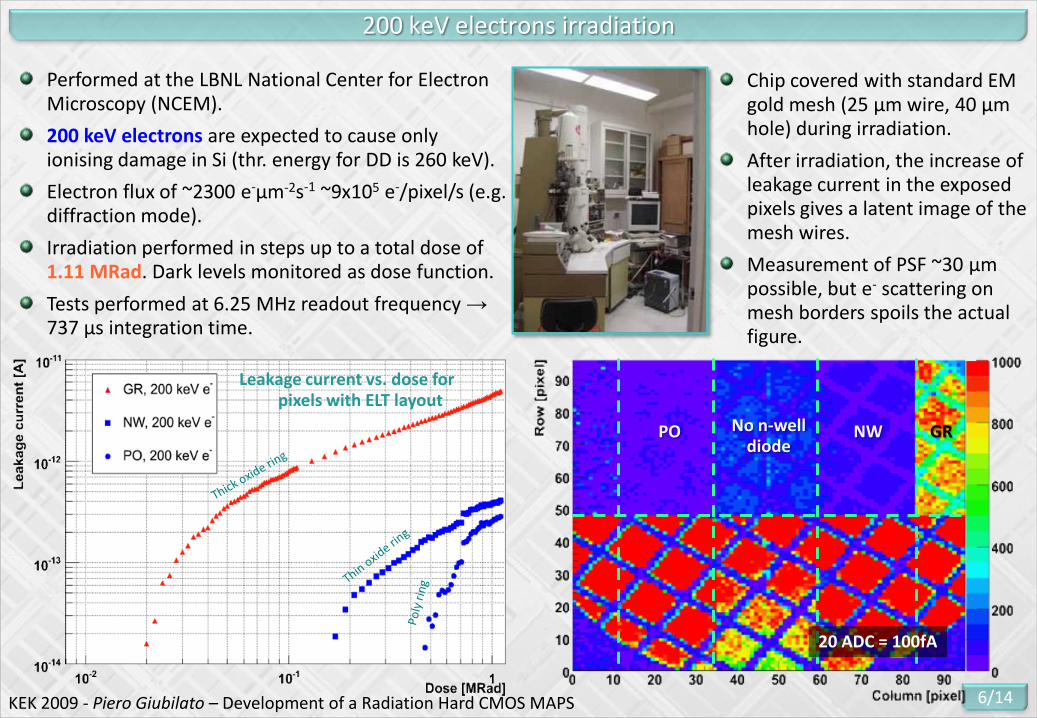
Performed at the LBNL National Center for Electron Microscopy (NCEM).
200 keV electrons are expected to cause only ionising damage in Si (thr. energy for DD is 260 keV).
Electron flux of ~2300 e-μm-2s-1 ~9x10⁵ e-/pixel/s (e.g. diffraction mode).
Irradiation performed in steps up to a total dose of 1.11 MRad. Dark levels monitored as dose function.
Tests performed at 6.25 MHz readout frequency → 737 μs integration time.
200 keV electrons irradiation
Chip covered with standard EM gold mesh (25 µm wire, 40 µm hole) during irradiation.
After irradiation, the increase of leakage current in the exposed pixels gives a latent image of the mesh wires.
Measurement of PSF ~30 μmpossible, but e- scattering on mesh borders spoils the actual figure.
Leakage current vs. dose for pixels with ELT layout
GRNWPO
20 ADC = 100fA
No n-welldiode
7/14KEK 2009 - Piero Giubilato – Development of a Radiation Hard CMOS MAPS
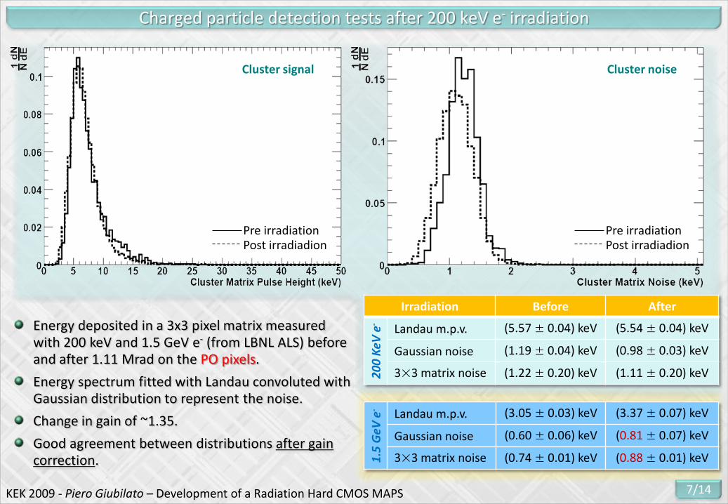
Energy deposited in a 3x3 pixel matrix measured with 200 keV and 1.5 GeV e- (from LBNL ALS) before and after 1.11 Mrad on the PO pixels.
Energy spectrum fitted with Landau convoluted with Gaussian distribution to represent the noise.
Change in gain of ~1.35.
Good agreement between distributions after gain correction.
Cluster signal Cluster noise
Charged particle detection tests after 200 keV e- irradiation
Irradiation Before After
20
0 K
eV e
-
Landau m.p.v. (5.57 ± 0.04) keV (5.54 ± 0.04) keV
Gaussian noise (1.19 ± 0.04) keV (0.98 ± 0.03) keV
3×3 matrix noise (1.22 ± 0.20) keV (1.11 ± 0.20) keV1
.5 G
eV e
- Landau m.p.v. (3.05 ± 0.03) keV (3.37 ± 0.07) keV
Gaussian noise (0.60 ± 0.06) keV (0.81± 0.07) keV
3×3 matrix noise (0.74 ± 0.01) keV (0.88± 0.01) keV
Pre irradiationPost irradiadion
Pre irradiationPost irradiadion
8/14KEK 2009 - Piero Giubilato – Development of a Radiation Hard CMOS MAPS
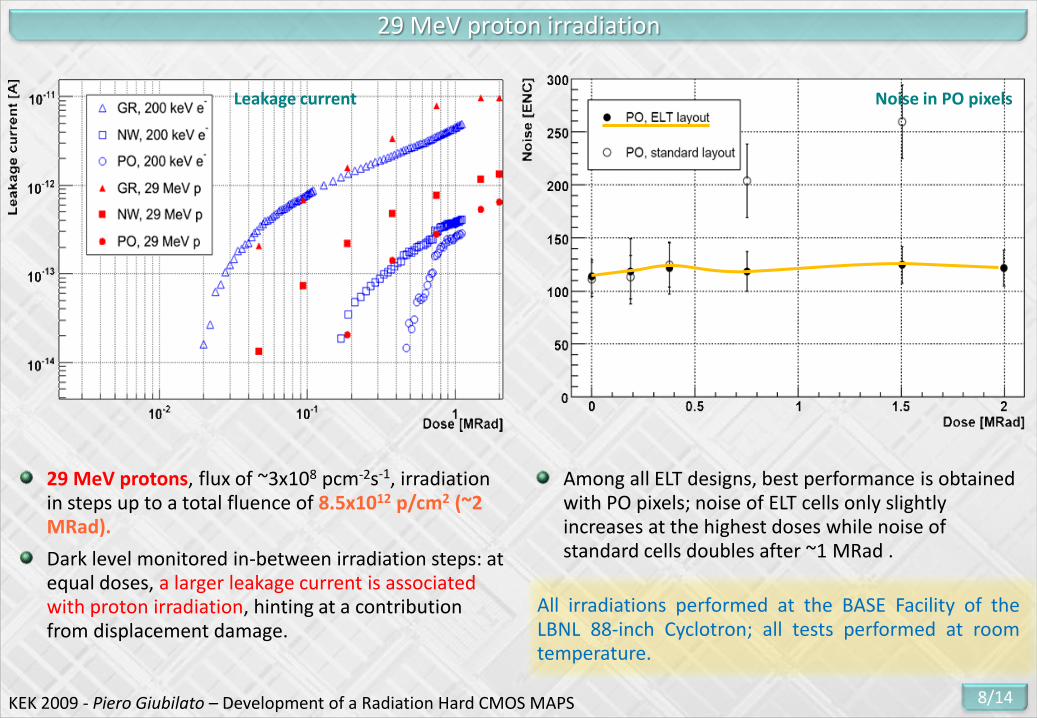
29 MeV protons, flux of ~3x10⁸ pcm-2s-1, irradiation in steps up to a total fluence of 8.5x10¹² p/cm2 (~2 MRad).
Dark level monitored in-between irradiation steps: at equal doses, a larger leakage current is associated with proton irradiation, hinting at a contribution from displacement damage.
29 MeV proton irradiation
All irradiations performed at the BASE Facility of theLBNL 88-inch Cyclotron; all tests performed at roomtemperature.
Noise in PO pixelsLeakage current
Among all ELT designs, best performance is obtained with PO pixels; noise of ELT cells only slightly increases at the highest doses while noise of standard cells doubles after ~1 MRad .
9/14KEK 2009 - Piero Giubilato – Development of a Radiation Hard CMOS MAPS
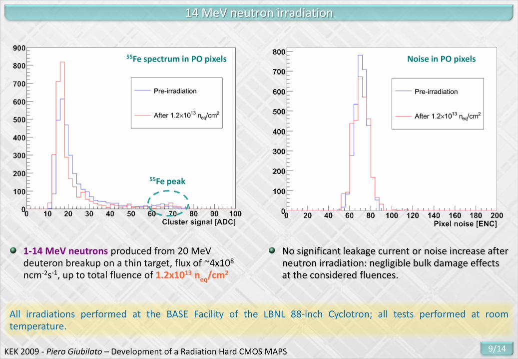
1-14 MeV neutrons produced from 20 MeVdeuteron breakup on a thin target, flux of ~4x10⁸
ncm-2s-1, up to total fluence of 1.2x10¹³ neq/cm2
14 MeV neutron irradiation
55Fe spectrum in PO pixels Noise in PO pixels
55Fe peak
All irradiations performed at the BASE Facility of the LBNL 88-inch Cyclotron; all tests performed at roomtemperature.
No significant leakage current or noise increase after neutron irradiation: negligible bulk damage effects at the considered fluences.
10/14KEK 2009 - Piero Giubilato – Development of a Radiation Hard CMOS MAPS
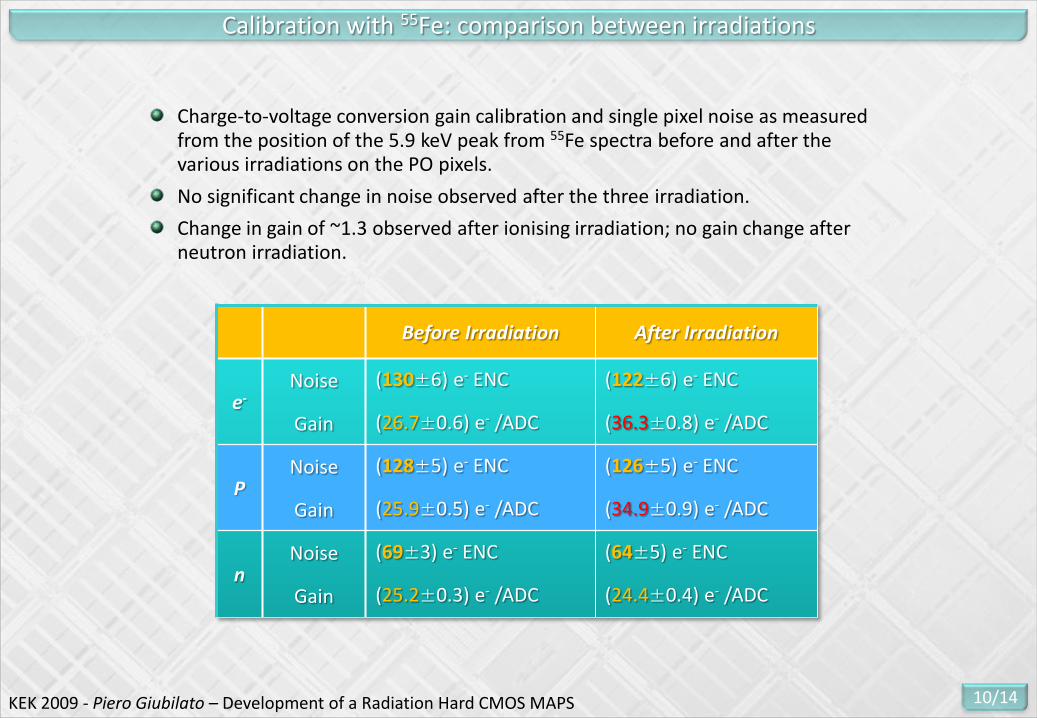
Charge-to-voltage conversion gain calibration and single pixel noise as measured from the position of the 5.9 keV peak from 55Fe spectra before and after the various irradiations on the PO pixels.
No significant change in noise observed after the three irradiation.
Change in gain of ~1.3 observed after ionising irradiation; no gain change after neutron irradiation.
Calibration with 55Fe: comparison between irradiations
Before Irradiation After Irradiation
e-Noise (130±6) e- ENC (122±6) e- ENC
Gain (26.7±0.6) e- /ADC (36.3±0.8) e- /ADC
PNoise (128±5) e- ENC (126±5) e- ENC
Gain (25.9±0.5) e- /ADC (34.9±0.9) e- /ADC
nNoise (69±3) e- ENC (64±5) e- ENC
Gain (25.2±0.3) e- /ADC (24.4±0.4) e- /ADC
11/14KEK 2009 - Piero Giubilato – Development of a Radiation Hard CMOS MAPS
75 µm
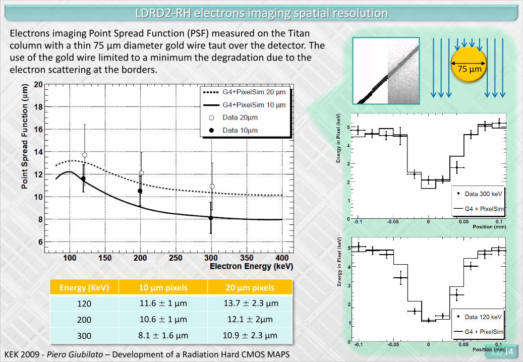
LDRD2-RH electrons imaging spatial resolution
Electrons imaging Point Spread Function (PSF) measured on the Titan column with a thin 75 µm diameter gold wire taut over the detector. The use of the gold wire limited to a minimum the degradation due to the electron scattering at the borders.
Energy (KeV) 10 µm pixels 20 µm pixels
120 11.6 ± 1 µm 13.7 ± 2.3 µm
200 10.6 ± 1 µm 12.1 ± 2µm
300 8.1 ± 1.6 µm 10.9 ± 2.3 µm
12/14KEK 2009 - Piero Giubilato – Development of a Radiation Hard CMOS MAPS
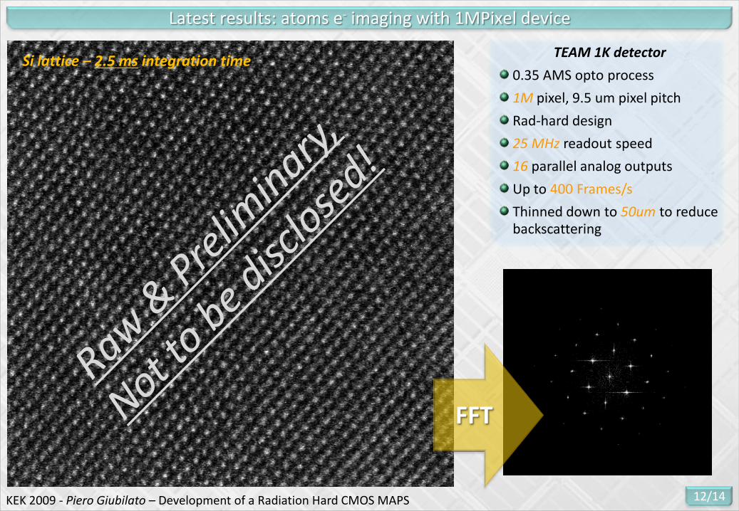
Latest results: atoms e- imaging with 1MPixel device
TEAM 1K detector
0.35 AMS opto process
1M pixel, 9.5 um pixel pitch
Rad-hard design
25 MHz readout speed
16 parallel analog outputs
Up to 400 Frames/s
Thinned down to 50um to reduce backscattering
FFT
Si lattice – 2.5 ms integration time
13/14KEK 2009 - Piero Giubilato – Development of a Radiation Hard CMOS MAPS
75 µm
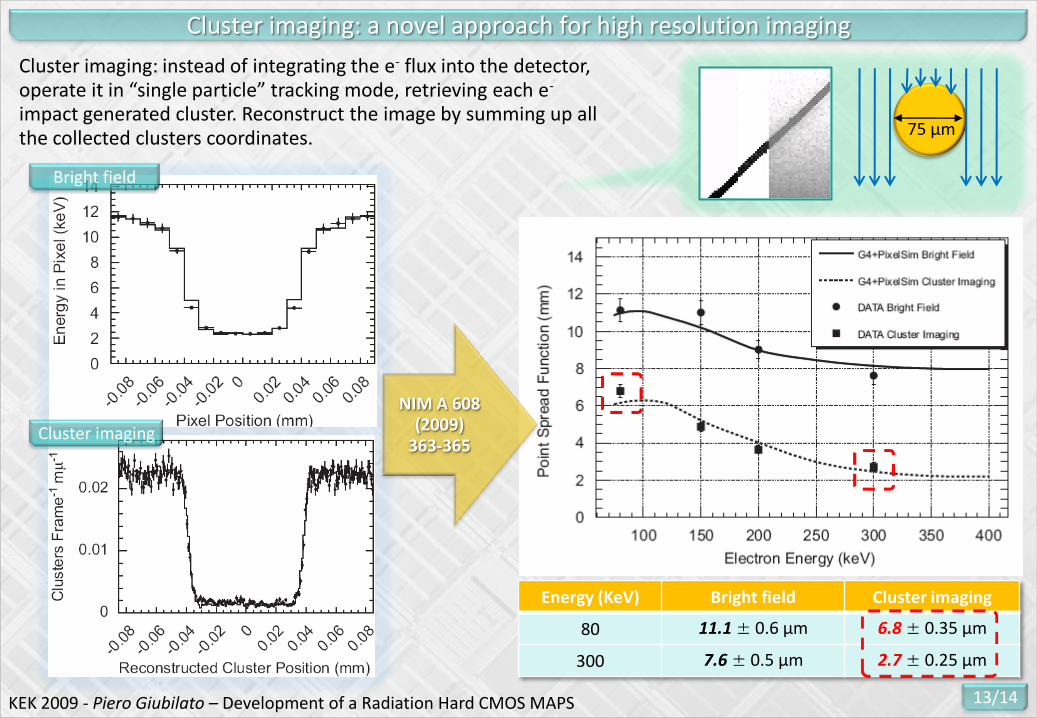
Cluster imaging: a novel approach for high resolution imaging
Cluster imaging: instead of integrating the e- flux into the detector, operate it in “single particle” tracking mode, retrieving each e-
impact generated cluster. Reconstruct the image by summing up all the collected clusters coordinates.
Energy (KeV) Bright field Cluster imaging
80 11.1± 0.6 µm 6.8± 0.35 µm
300 7.6± 0.5 µm 2.7± 0.25 µm
NIM A 608(2009)
363-365
Bright field
Cluster imaging
14/14KEK 2009 - Piero Giubilato – Development of a Radiation Hard CMOS MAPS
A CMOS monolithic pixel sensor with optimized layout of the pixel cell for improved radiation tolerance has been designed and tested up to 2 MRad ionising radiation and ~1013 neq/cm2
non-ionising fluence.
The chip implements transistors designed both with and without ELT rules, and different layout optimizations of the charge collecting diodes.
The tests performed show an improved performance of pixels with ELT transistors, a thinner oxide on top of the diode surface and guard-rings around the diodes.
This pixel layout has been implemented in a larger scale prototype deployed as a high-resolution (1 MPixel to 4 MPixel), fast (400 frame/s) and radiation-hard detector for the TEAM electron microscope at the LBNL National Centre for Electron Microscopy.
Conclusions


![Power Efficient CMOS Full Adders with Reduced Transistor Count · The TGA full adder [5] using 20 transistors is based on CMOS transmission gates and CMOS inverters. It ... In TFA](https://static.fdocument.org/doc/165x107/5c01a10709d3f20f068d0c17/power-efficient-cmos-full-adders-with-reduced-transistor-count-the-tga-full.jpg)