DAC in 65-nm CMOS
6
An 8-GS/s 200-MHz Bandwidth 68-mW ΔΣ DAC in 65-nm CMOS Ameya Bhide, Omid Esmailzadeh Najari, Behzad Mesgarzadeh and Atila Alvandpour Linköping University Post Print N.B.: When citing this work, cite the original article. ©2013 IEEE. Personal use of this material is permitted. However, permission to reprint/republish this material for advertising or promotional purposes or for creating new collective works for resale or redistribution to servers or lists, or to reuse any copyrighted component of this work in other works must be obtained from the IEEE. Ameya Bhide, Omid Esmailzadeh Najari, Behzad Mesgarzadeh and Atila Alvandpour, An 8- GS/s 200-MHz Bandwidth 68-mW ΔΣ DAC in 65-nm CMOS, 2013, IEEE Transactions on Circuits and Systems - II - Express Briefs, (60), 7, 387-391. http://dx.doi.org/10.1109/TCSII.2013.2258272 Postprint available at: Linköping University Electronic Press http://urn.kb.se/resolve?urn=urn:nbn:se:liu:diva-96713
Transcript of DAC in 65-nm CMOS
An 8-GS/s 200-MHz Bandwidth 68-mW ΔΣ
DAC in 65-nm CMOS
Ameya Bhide, Omid Esmailzadeh Najari, Behzad Mesgarzadeh and Atila Alvandpour
Linköping University Post Print
N.B.: When citing this work, cite the original article.
©2013 IEEE. Personal use of this material is permitted. However, permission to
reprint/republish this material for advertising or promotional purposes or for creating new
collective works for resale or redistribution to servers or lists, or to reuse any copyrighted
component of this work in other works must be obtained from the IEEE.
Ameya Bhide, Omid Esmailzadeh Najari, Behzad Mesgarzadeh and Atila Alvandpour, An 8-
GS/s 200-MHz Bandwidth 68-mW ΔΣ DAC in 65-nm CMOS, 2013, IEEE Transactions on
Circuits and Systems - II - Express Briefs, (60), 7, 387-391.
http://dx.doi.org/10.1109/TCSII.2013.2258272
Postprint available at: Linköping University Electronic Press
http://urn.kb.se/resolve?urn=urn:nbn:se:liu:diva-96713
1
An 8-GS/s 200-MHz Bandwidth 68-mW ∆Σ DACin 65-nm CMOS
Ameya Bhide, Student Member, IEEE, Omid Esmailzadeh Najari, Student Member, IEEE,Behzad Mesgarzadeh, Member, IEEE, and Atila Alvandpour, Senior Member, IEEE
Abstract—This paper presents an 8-GS/s, 12-bit input ∆Σ DACwith 200-MHz bandwidth in 65-nm CMOS. The high samplingrate is achieved by a two-channel interleaved MASH 1-1 digital∆Σ modulator with 3-bit output, resulting in a highly digitalDAC with only seven current cells. The two-channel interleavingallows the use of a single clock for both the logic and the finalmultiplexing. This requires each channel to operate at half thesampling rate, which is enabled by a high-speed pipelined MASHstructure with robust static logic. Measurement results show thatthe DAC achieves 200-MHz bandwidth, 26-dB SNDR and -57-dBcIMD3, with a power consumption of 68-mW at 1-V digital and1.2-V analog supplies. This architecture shows potential for usein transmitter baseband for wideband wireless communication.
Index Terms—Digital ∆Σ modulator (DDSM), digital-to-analog converter (DAC), time-interleaving, oversampling, MASH.
I. INTRODUCTION
OVERSAMPLED ∆Σ DACs have been reported in all-digital [1], “almost” digital [2] and RFDAC [3], [4]
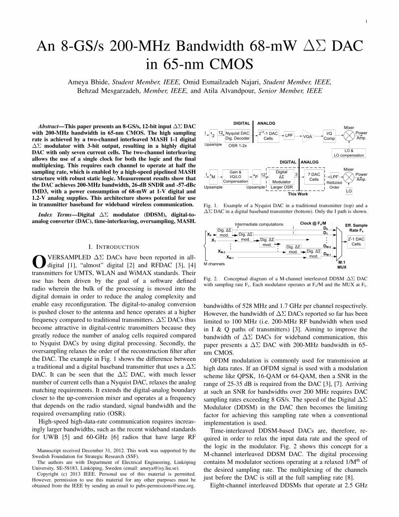
transmitters for UMTS, WLAN and WiMAX standards. Theiruse has been driven by the goal of a software definedradio wherein the bulk of the processing is moved into thedigital domain in order to reduce the analog complexity andenable easy reconfiguration. The digital-to-analog conversionis pushed closer to the antenna and hence operates at a higherfrequency compared to traditional transmitters. ∆Σ DACs thusbecome attractive in digital-centric transmitters because theygreatly reduce the number of analog cells required comparedto Nyquist DACs by using digital processing. Secondly, theoversampling relaxes the order of the reconstruction filter afterthe DAC. The example in Fig. 1 shows the difference betweena traditional and a digital baseband transmitter that uses a ∆ΣDAC. It can be seen that the ∆Σ DAC, with much lessernumber of current cells than a Nyquist DAC, relaxes the analogmatching requirements. It extends the digital-analog boundarycloser to the up-conversion mixer and operates at a frequencythat depends on the radio standard, signal bandwidth and therequired oversampling ratio (OSR).
High-speed high-data-rate communication requires increas-ingly larger bandwidths, such as the recent wideband standardsfor UWB [5] and 60-GHz [6] radios that have large RF
Manuscript received December 31, 2012. This work was supported by theSwedish Foundation for Strategic Research (SSF).
The authors are with Department of Electrical Engineering, LinkopingUniversity, SE-58183, Linkoping, Sweden (email: [email protected]).
Copyright (c) 2013 IEEE. Personal use of this material is permitted.However, permission to use this material for any other purposes must beobtained from the IEEE by sending an email to [email protected].
2Nyquist DAC
Dig. Decoder2
12-1 DAC
CellsLPF
LO &
LO compensation
I/Q
CompVGA
Mixer
I
DIGITAL ANALOG
M
Gain &
I/Q/LO
Compensation
12
12Digital
û
Modulator
7 DAC
Cells
LO
Mixer
DIGITAL ANALOG
This Work
PI
OSR 1-2x
Larger OSR
LPF3
Upsample
Power
Amp.
Power
Amp.
Upsample UpsampleReduced
Order
Fig. 1. Example of a Nyquist DAC in a traditional transmitter (top) and a∆Σ DAC in a digital baseband transmitter (bottom). Only the I path is shown.
Dig. û
mod.
Dig. û
mod.2
i-1 DAC
Cells
X0
X1
XM-2
XM-1
Clock @ Fs/M Eff. Sample
Rate Fs
M:1
MUX
Dig. û
mod.
Dig. û
mod.
i
i
Intermediate computationsD0
D1
DM-2
DM-1
Dig. û
mod.
M channels
Fig. 2. Conceptual diagram of a M-channel interleaved DDSM ∆Σ DACwith sampling rate Fs. Each modulator operates at Fs/M and the MUX at Fs.
bandwidths of 528 MHz and 1.7 GHz per channel respectively.However, the bandwidth of ∆Σ DACs reported so far has beenlimited to 100 MHz (i.e. 200-MHz RF bandwidth when usedin I & Q paths of transmitters) [3]. Aiming to improve thebandwidth of ∆Σ DACs for wideband communication, thispaper presents a ∆Σ DAC with 200-MHz bandwidth in 65-nm CMOS.
OFDM modulation is commonly used for transmission athigh data rates. If an OFDM signal is used with a modulationscheme like QPSK, 16-QAM or 64-QAM, then a SNR in therange of 25-35 dB is required from the DAC [3], [7]. Arrivingat such an SNR for bandwidths over 200 MHz requires DACsampling rates exceeding 8 GS/s. The speed of the Digital ∆ΣModulator (DDSM) in the DAC then becomes the limitingfactor for achieving this sampling rate when a conventionalimplementation is used.
Time-interleaved DDSM-based DACs are, therefore, re-quired in order to relax the input data rate and the speed ofthe logic in the modulator. Fig. 2 shows this concept for aM-channel interleaved DDSM DAC. The digital processingcontains M modulator sections operating at a relaxed 1/Mth ofthe desired sampling rate. The multiplexing of the channelsjust before the DAC is still at the full sampling rate [8].
Eight-channel interleaved DDSMs that operate at 2.5 GHz
2
decoder
clock
divider
Fs clock domain
Fs/8 clock
domain
D0
D1
From
DDSM
DACD0
D1
DAC
From
DDSM
clk @ Fs/2
D6
D7
Fs
CML Phase
Rotators @ Fs/4
DAC
DAC
D0
D1
D2
D3
clk @ Fs/2
(a) (b) (c)
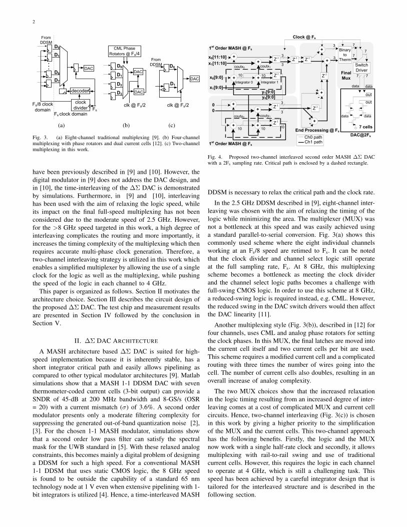
Fig. 3. (a) Eight-channel traditional multiplexing [9]. (b) Four-channelmultiplexing with phase rotators and dual current cells [12]. (c) Two-channelmultiplexing in this work.
have been previously described in [9] and [10]. However, thedigital modulator in [9] does not address the DAC design, andin [10], the time-interleaving of the ∆Σ DAC is demonstratedby simulations. Furthermore, in [9] and [10], interleavinghas been used with the aim of relaxing the logic speed, whileits impact on the final full-speed multiplexing has not beenconsidered due to the moderate speed of 2.5 GHz. However,for the >8 GHz speed targeted in this work, a high degree ofinterleaving complicates the routing and more importantly, itincreases the timing complexity of the multiplexing which thenrequires accurate multi-phase clock generation. Therefore, atwo-channel interleaving strategy is utilized in this work whichenables a simplified multiplexer by allowing the use of a singleclock for the logic as well as the multiplexing, while pushingthe speed of the logic in each channel to 4 GHz.
This paper is organized as follows. Section II motivates thearchitecture choice. Section III describes the circuit design ofthe proposed ∆Σ DAC. The test chip and measurement resultsare presented in Section IV followed by the conclusion inSection V.
II. ∆Σ DAC ARCHITECTURE
A MASH architecture based ∆Σ DAC is suited for high-speed implementation because it is inherently stable, has ashort integrator critical path and easily allows pipelining ascompared to other typical modulator architectures [9]. Matlabsimulations show that a MASH 1-1 DDSM DAC with seventhermometer-coded current cells (3-bit output) can provide aSNDR of 45-dB at 200 MHz bandwidth and 8-GS/s (OSR= 20) with a current mismatch (σ) of 3.6%. A second ordermodulator presents only a moderate filtering complexity forsuppressing the generated out-of-band quantization noise [2],[3]. For the chosen 1-1 MASH modulator, simulations showthat a second order low pass filter can satisfy the spectralmask for the UWB standard in [5]. With these relaxed analogconstraints, this becomes mainly a digital problem of designinga DDSM for such a high speed. For a conventional MASH1-1 DDSM that uses static CMOS logic, the 8 GHz speedis found to be outside the capability of a standard 65 nmtechnology node at 1 V even when extensive pipelining with 1-bit integrators is utilized [4]. Hence, a time-interleaved MASH
++-
Z-1
++
-
Z-1 Z-1
Z-1
+
+
3
3
7
7
7
Clock @ Fs
End Processing @ Fs
Final
Mux
Switch
Driver
7 7
data data
DAC@2Fs
Binary
to
Therm x0[11:10]
+ +Z-110
x0[9:0]
x1[9:0]
+
+
10
x1[11:10]coutx0 coutx1
Z-1
3
3
+ +Z-1
10
y1[9:0]
+
+
10 10
couty0 couty1
Z-1
3
3
y0[9:0]
0
0
out
data data
out
1st
Order MASH @ Fs
1st
Order MASH @ Fs
Ch0 pathCh1 path
Integrator 0 Integrator 1
7 cells
Fig. 4. Proposed two-channel interleaved second order MASH ∆Σ DACwith a 2Fs sampling rate. Critical path is enclosed by a dashed rectangle.
DDSM is necessary to relax the critical path and the clock rate.
In the 2.5 GHz DDSM described in [9], eight-channel inter-leaving was chosen with the aim of relaxing the timing of thelogic while minimizing the area. The multiplexer (MUX) wasnot a bottleneck at this speed and was easily achieved usinga standard parallel-to-serial conversion. Fig. 3(a) shows thiscommonly used scheme where the eight individual channelsworking at an Fs/8 speed are retimed to Fs. It can be notedthat the clock divider and channel select logic still operateat the full sampling rate, Fs. At 8 GHz, this multiplexingscheme becomes a bottleneck as meeting the clock dividerand the channel select logic paths becomes a challenge withfull-swing CMOS logic. In order to use this scheme at 8 GHz,a reduced-swing logic is required instead, e.g. CML. However,the reduced swing in the DAC switch drivers would then affectthe DAC linearity [11].
Another multiplexing style (Fig. 3(b)), described in [12] forfour channels, uses CML and analog phase rotators for settingthe clock phases. In this MUX, the final latches are moved intothe current cell itself and two current cells per bit are used.This scheme requires a modified current cell and a complicatedrouting with three times the number of wires going into thecell. The number of current cells also doubles, resulting in anoverall increase of analog complexity.
The two MUX choices show that the increased relaxationin the logic timing resulting from an increased degree of inter-leaving comes at a cost of complicated MUX and current cellcircuits. Hence, two-channel interleaving (Fig. 3(c)) is chosenin this work by giving a higher priority to the simplificationof the MUX and the current cells. This two-channel approachhas the following benefits. Firstly, the logic and the MUXnow work with a single half-rate clock and secondly, it allowsmultiplexing with rail-to-rail swing and use of traditionalcurrent cells. However, this requires the logic in each channelto operate at 4 GHz, which is still a challenging task. Thisspeed has been achieved by a careful integrator design that istailored for the interleaved structure and is described in thefollowing section.
3
x0[0]
x0[1]
rst+
a
b
sum
ci
co co+
a
b
ci
co co
a D Q
+
a
b
ci
co
ci
+
a
b
ci
co
a
ci
rstD Q
clk
rst rst
D
Q
D
Q
4 X 2-Bit Integrator
Pipelines
3-Bit Forward Pipeline
x1[1]
x1[0]
cinx0 cinx1
A1
A2 A4
A3
coutx0 coutx1
3
2-Bit Integrator
Pipeline ± 8FFs
To end processing
clk
clkclk
clk
clk
clk
clk
sum
sum
sum
sum
2 FFs
2 FFs
D Q
clkclk
rst
D Q
clkclk
rst
Integrator 0 / Ch0 Path Integrator 1/ Ch1 Path
y1[0]
y0[0]
y1[1]
y0[1]
sum
To 2nd
MASH Stage
y0[9:2]
y1[9:2]x0[11:2]
x1[11:2]
Data Align
88 FFs
To 2nd
MASH
Stage
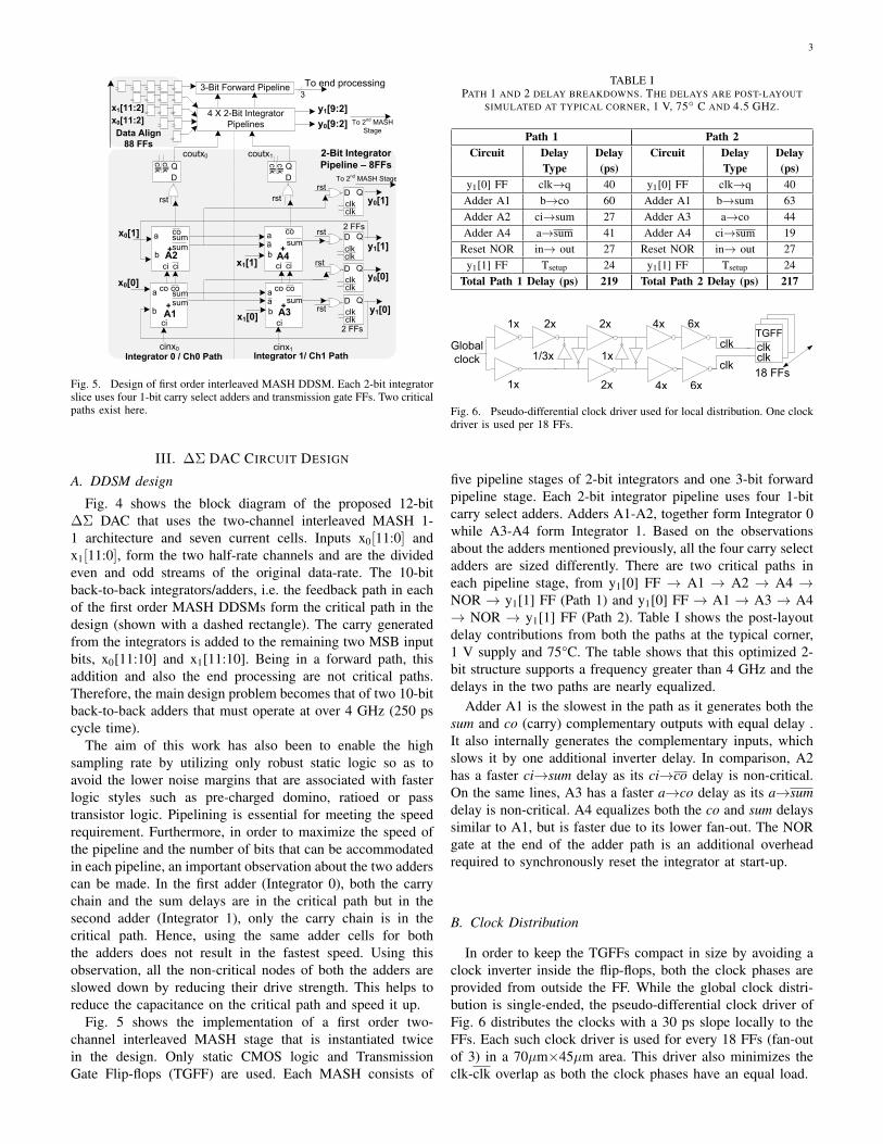
Fig. 5. Design of first order interleaved MASH DDSM. Each 2-bit integratorslice uses four 1-bit carry select adders and transmission gate FFs. Two criticalpaths exist here.
III. ∆Σ DAC CIRCUIT DESIGN
A. DDSM design
Fig. 4 shows the block diagram of the proposed 12-bit∆Σ DAC that uses the two-channel interleaved MASH 1-1 architecture and seven current cells. Inputs x0[11:0] andx1[11:0], form the two half-rate channels and are the dividedeven and odd streams of the original data-rate. The 10-bitback-to-back integrators/adders, i.e. the feedback path in eachof the first order MASH DDSMs form the critical path in thedesign (shown with a dashed rectangle). The carry generatedfrom the integrators is added to the remaining two MSB inputbits, x0[11:10] and x1[11:10]. Being in a forward path, thisaddition and also the end processing are not critical paths.Therefore, the main design problem becomes that of two 10-bitback-to-back adders that must operate at over 4 GHz (250 pscycle time).
The aim of this work has also been to enable the highsampling rate by utilizing only robust static logic so as toavoid the lower noise margins that are associated with fasterlogic styles such as pre-charged domino, ratioed or passtransistor logic. Pipelining is essential for meeting the speedrequirement. Furthermore, in order to maximize the speed ofthe pipeline and the number of bits that can be accommodatedin each pipeline, an important observation about the two adderscan be made. In the first adder (Integrator 0), both the carrychain and the sum delays are in the critical path but in thesecond adder (Integrator 1), only the carry chain is in thecritical path. Hence, using the same adder cells for boththe adders does not result in the fastest speed. Using thisobservation, all the non-critical nodes of both the adders areslowed down by reducing their drive strength. This helps toreduce the capacitance on the critical path and speed it up.
Fig. 5 shows the implementation of a first order two-channel interleaved MASH stage that is instantiated twicein the design. Only static CMOS logic and TransmissionGate Flip-flops (TGFF) are used. Each MASH consists of
TABLE IPATH 1 AND 2 DELAY BREAKDOWNS. THE DELAYS ARE POST-LAYOUT
SIMULATED AT TYPICAL CORNER, 1 V, 75 C AND 4.5 GHZ.
Path 1 Path 2Circuit Delay Delay Circuit Delay Delay
Type (ps) Type (ps)y1[0] FF clk→q 40 y1[0] FF clk→q 40
Adder A1 b→co 60 Adder A1 b→sum 63Adder A2 ci→sum 27 Adder A3 a→co 44Adder A4 a→sum 41 Adder A4 ci→sum 19
Reset NOR in→ out 27 Reset NOR in→ out 27y1[1] FF Tsetup 24 y1[1] FF Tsetup 24
Total Path 1 Delay (ps) 219 Total Path 2 Delay (ps) 217
Global
clock
1x
2x
1/3x
clk
2x
1x
4x
1x
2x
4x
clkclk
TGFF
18 FFs
6x
6x
clk
Fig. 6. Pseudo-differential clock driver used for local distribution. One clockdriver is used per 18 FFs.
five pipeline stages of 2-bit integrators and one 3-bit forwardpipeline stage. Each 2-bit integrator pipeline uses four 1-bitcarry select adders. Adders A1-A2, together form Integrator 0while A3-A4 form Integrator 1. Based on the observationsabout the adders mentioned previously, all the four carry selectadders are sized differently. There are two critical paths ineach pipeline stage, from y1[0] FF → A1 → A2 → A4 →NOR → y1[1] FF (Path 1) and y1[0] FF → A1 → A3 → A4→ NOR → y1[1] FF (Path 2). Table I shows the post-layoutdelay contributions from both the paths at the typical corner,1 V supply and 75°C. The table shows that this optimized 2-bit structure supports a frequency greater than 4 GHz and thedelays in the two paths are nearly equalized.
Adder A1 is the slowest in the path as it generates both thesum and co (carry) complementary outputs with equal delay .It also internally generates the complementary inputs, whichslows it by one additional inverter delay. In comparison, A2has a faster ci→sum delay as its ci→co delay is non-critical.On the same lines, A3 has a faster a→co delay as its a→sumdelay is non-critical. A4 equalizes both the co and sum delayssimilar to A1, but is faster due to its lower fan-out. The NORgate at the end of the adder path is an additional overheadrequired to synchronously reset the integrator at start-up.
B. Clock Distribution
In order to keep the TGFFs compact in size by avoiding aclock inverter inside the flip-flops, both the clock phases areprovided from outside the FF. While the global clock distri-bution is single-ended, the pseudo-differential clock driver ofFig. 6 distributes the clocks with a 30 ps slope locally to theFFs. Each such clock driver is used for every 18 FFs (fan-outof 3) in a 70µm×45µm area. This driver also minimizes theclk-clk overlap as both the clock phases have an equal load.
4
D Q
D Q
D Q
Binary
To
Therm
Ch0
Ch1 clk clk
clkclk
half-cycle path
half-cycle path
Clock
Distrib.
Final MUX per current cell
4-stage buffered clock
Clock Fs
DAC Current Cell
Ch1_L
Ch0_H
Switch
Driver
M1
M2 M3
M4 M5
30/0.13
30/0.13
20/0.06data
Vb1
Vb2
Iout
data
Iout
A1 A2 A3 A4
B1 B2 B3 B4
A1 B1 A2 B2 A3 B3 A4 B4
Clock Fs
Ch0_H
Ch1_L
DAC
input
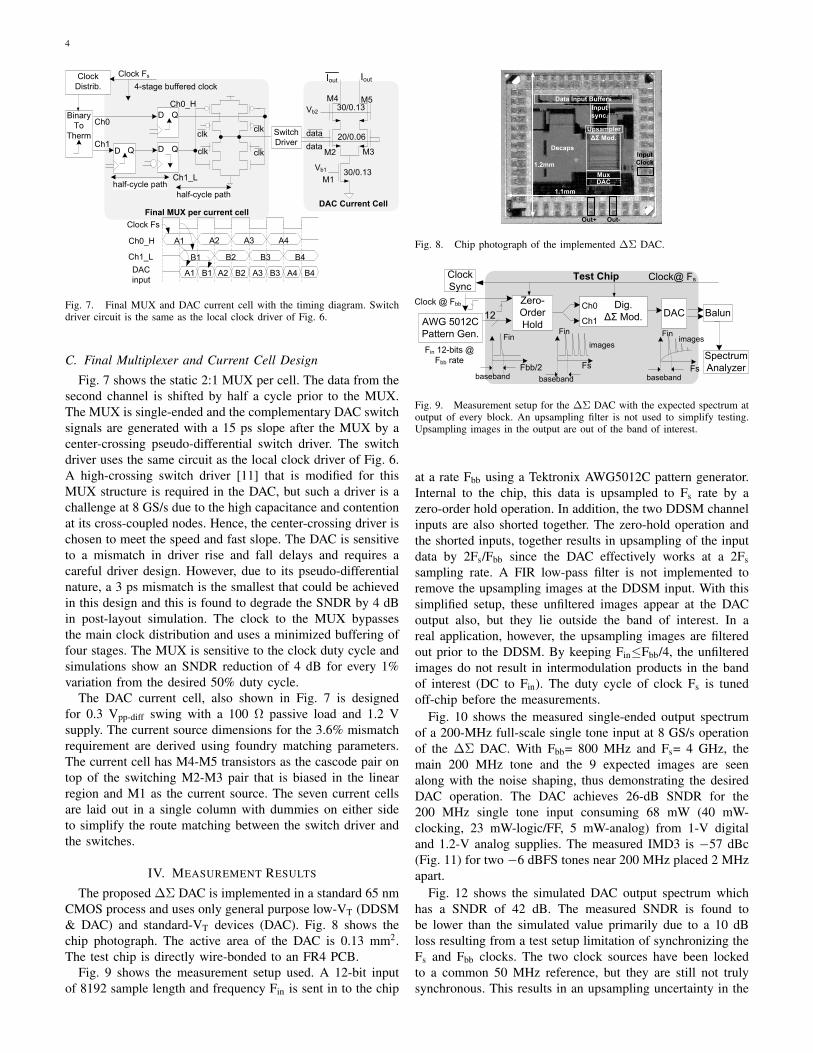
Fig. 7. Final MUX and DAC current cell with the timing diagram. Switchdriver circuit is the same as the local clock driver of Fig. 6.
C. Final Multiplexer and Current Cell Design
Fig. 7 shows the static 2:1 MUX per cell. The data from thesecond channel is shifted by half a cycle prior to the MUX.The MUX is single-ended and the complementary DAC switchsignals are generated with a 15 ps slope after the MUX by acenter-crossing pseudo-differential switch driver. The switchdriver uses the same circuit as the local clock driver of Fig. 6.A high-crossing switch driver [11] that is modified for thisMUX structure is required in the DAC, but such a driver is achallenge at 8 GS/s due to the high capacitance and contentionat its cross-coupled nodes. Hence, the center-crossing driver ischosen to meet the speed and fast slope. The DAC is sensitiveto a mismatch in driver rise and fall delays and requires acareful driver design. However, due to its pseudo-differentialnature, a 3 ps mismatch is the smallest that could be achievedin this design and this is found to degrade the SNDR by 4 dBin post-layout simulation. The clock to the MUX bypassesthe main clock distribution and uses a minimized buffering offour stages. The MUX is sensitive to the clock duty cycle andsimulations show an SNDR reduction of 4 dB for every 1%variation from the desired 50% duty cycle.
The DAC current cell, also shown in Fig. 7 is designedfor 0.3 Vpp-diff swing with a 100 Ω passive load and 1.2 Vsupply. The current source dimensions for the 3.6% mismatchrequirement are derived using foundry matching parameters.The current cell has M4-M5 transistors as the cascode pair ontop of the switching M2-M3 pair that is biased in the linearregion and M1 as the current source. The seven current cellsare laid out in a single column with dummies on either sideto simplify the route matching between the switch driver andthe switches.
IV. MEASUREMENT RESULTS
The proposed ∆Σ DAC is implemented in a standard 65 nmCMOS process and uses only general purpose low-VT (DDSM& DAC) and standard-VT devices (DAC). Fig. 8 shows thechip photograph. The active area of the DAC is 0.13 mm2.The test chip is directly wire-bonded to an FR4 PCB.
Fig. 9 shows the measurement setup used. A 12-bit inputof 8192 sample length and frequency Fin is sent in to the chip
Upsampler
ûMod.
DAC
Decaps
Data Input Buffers
Input
sync.
Mux
Input
Clock1.2mm
1.1mm
Out+ Out-
Fig. 8. Chip photograph of the implemented ∆Σ DAC.
AWG 5012C
Pattern Gen.
Fin 12-bits @
Fbb rate
Zero-
Order
Hold
Ch0
Ch1DAC
Clock@ Fs
Balun
Spectrum
AnalyzerFbb/2 Fs Fsbaseband
Test Chip
baseband
imagesFin
Clock @ Fbb
Fin Fin images
baseband
12Dig.
ûMod.
Clock
Sync
Fig. 9. Measurement setup for the ∆Σ DAC with the expected spectrum atoutput of every block. An upsampling filter is not used to simplify testing.Upsampling images in the output are out of the band of interest.
at a rate Fbb using a Tektronix AWG5012C pattern generator.Internal to the chip, this data is upsampled to Fs rate by azero-order hold operation. In addition, the two DDSM channelinputs are also shorted together. The zero-hold operation andthe shorted inputs, together results in upsampling of the inputdata by 2Fs/Fbb since the DAC effectively works at a 2Fssampling rate. A FIR low-pass filter is not implemented toremove the upsampling images at the DDSM input. With thissimplified setup, these unfiltered images appear at the DACoutput also, but they lie outside the band of interest. In areal application, however, the upsampling images are filteredout prior to the DDSM. By keeping Fin≤Fbb/4, the unfilteredimages do not result in intermodulation products in the bandof interest (DC to Fin). The duty cycle of clock Fs is tunedoff-chip before the measurements.
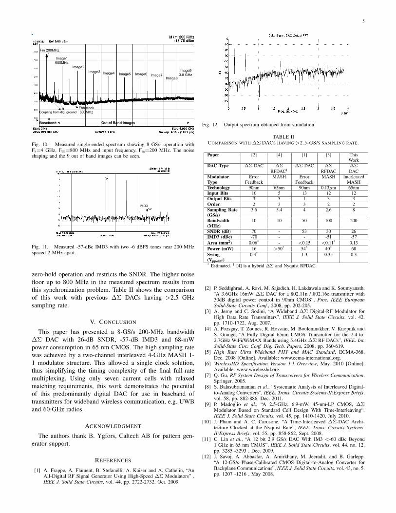
Fig. 10 shows the measured single-ended output spectrumof a 200-MHz full-scale single tone input at 8 GS/s operationof the ∆Σ DAC. With Fbb= 800 MHz and Fs= 4 GHz, themain 200 MHz tone and the 9 expected images are seenalong with the noise shaping, thus demonstrating the desiredDAC operation. The DAC achieves 26-dB SNDR for the200 MHz single tone input consuming 68 mW (40 mW-clocking, 23 mW-logic/FF, 5 mW-analog) from 1-V digitaland 1.2-V analog supplies. The measured IMD3 is −57 dBc(Fig. 11) for two −6 dBFS tones near 200 MHz placed 2 MHzapart.
Fig. 12 shows the simulated DAC output spectrum whichhas a SNDR of 42 dB. The measured SNDR is found tobe lower than the simulated value primarily due to a 10 dBloss resulting from a test setup limitation of synchronizing theFs and Fbb clocks. The two clock sources have been lockedto a common 50 MHz reference, but they are still not trulysynchronous. This results in an upsampling uncertainty in the
5
Image1
600MHz
Fbb clock
800MHz
Fin 200MHz
Baseband
Image2Image9
3.8 GHzImage3 Image4 Image5 Image6 Image7
Image8
Out of Band Images
Coupling from dig. ground
Fig. 10. Measured single-ended spectrum showing 8 GS/s operation withFs=4 GHz, Fbb=800 MHz and input frequency, Fin=200 MHz. The noiseshaping and the 9 out of band images can be seen.
IMD3
Fig. 11. Measured -57-dBc IMD3 with two -6 dBFS tones near 200 MHzspaced 2 MHz apart.
zero-hold operation and restricts the SNDR. The higher noisefloor up to 800 MHz in the measured spectrum results fromthis synchronization problem. Table II shows the comparisonof this work with previous ∆Σ DACs having >2.5 GHzsampling rate.
V. CONCLUSION
This paper has presented a 8-GS/s 200-MHz bandwidth∆Σ DAC with 26-dB SNDR, -57-dB IMD3 and 68-mWpower consumption in 65 nm CMOS. The high sampling ratewas achieved by a two-channel interleaved 4-GHz MASH 1-1 modulator structure. This allowed a single clock solution,thus simplifying the timing complexity of the final full-ratemultiplexing. Using only seven current cells with relaxedmatching requirements, this work demonstrates the potentialof this predominantly digital DAC for use in baseband oftransmitters for wideband wireless communication, e.g. UWBand 60-GHz radios.
ACKNOWLEDGMENT
The authors thank B. Ygfors, Caltech AB for pattern gen-erator support.
REFERENCES
[1] A. Frappe, A. Flament, B. Stefanelli, A. Kaiser and A. Cathelin, “AnAll-Digital RF Signal Generator Using High-Speed ∆Σ Modulators” ,IEEE J. Solid State Circuits, vol. 44, pp. 2722-2732, Oct. 2009.
Fig. 12. Output spectrum obtained from simulation.
TABLE IICOMPARISON WITH ∆Σ DACS HAVING >2.5-GS/S SAMPLING RATE.
Paper [2] [4] [1] [3] ThisWork
DAC Type ∆Σ DAC ∆Σ ∆Σ DAC ∆Σ ∆ΣRFDAC1 RFDAC DAC
Modulator Error MASH Error MASH InterleavedType Feedback Feedback MASHTechnology 90nm 65nm 90nm 0.13µm 65nmInput Bits 10 5 13 12 12Output Bits 3 3 1 3 3Order 2 3 3 2 2Sampling Rate 3.6 5.4 4 2.6 8(GS/s)Bandwidth 10 10 50 100 200(MHz)SNDR (dB) 70 - 53 30 26IMD3 (dBc) -70 - - -51 -57Area (mm2) 0.06* - <0.15 <0.11* 0.13Power (mW) 16 >50* 54* 40* 68Swing 0.3* - 1.3 0.35 0.3(Vpp-diff)* Estimated. 1 [4] is a hybrid ∆Σ and Nyquist RFDAC.
[2] P. Seddighrad, A. Ravi, M. Sajadieh, H. Lakdawala and K. Soumyanath,“A 3.6GHz 16mW ∆Σ DAC for a 802.11n / 802.16e transmitter with30dB digital power control in 90nm CMOS“, Proc. IEEE EuropeanSolid-State Circuits Conf., 2008, pp. 202-205.
[3] A. Jerng and C. Sodini, “A Wideband ∆Σ Digital-RF Modulator forHigh Data Rate Transmitters”, IEEE J. Solid State Circuits, vol. 42,pp. 1710-1722, Aug. 2007.
[4] A. Pozsgay, T. Zounes, R. Hossain, M. Boulemnakher, V. Knopnik andS. Grange, “A Fully Digital 65nm CMOS Transmitter for the 2.4-to-2.7GHz WiFi/WiMAX Bands using 5.4GHz ∆Σ RF DACs”, IEEE. Int.Solid-State Circ. Conf. Dig. Tech. Papers, 2008, pp. 360-619.
[5] High Rate Ultra Wideband PHY and MAC Standard, ECMA-368,Dec. 2008 [Online]. Available: www.ecma-international.org.
[6] WirelessHD Specification Version 1.1 Overview, May. 2010 [Online].Available: www.wirelesshd.org.
[7] Q. Gu, RF System Design of Transceivers for Wireless Communication,Springer, 2005.
[8] S. Balasubramanian et al., “Systematic Analysis of Interleaved Digital-to-Analog Converters”, IEEE. Trans. Circuits Systems-II:Express Briefs,vol. 58, pp. 882-886, Dec. 2011.
[9] P. Madoglio et al., “A 2.5-GHz, 6.9-mW, 45-nm-LP CMOS, ∆ΣModulator Based on Standard Cell Design With Time-Interleaving“,IEEE J. Solid State Circuits, vol. 45, pp. 1410-1420, July 2010.
[10] J. Pham and A. C. Carusone, “A Time-Interleaved ∆Σ-DAC Archi-tecture Clocked at the Nyquist Rate”, IEEE. Trans. Circuits Systems-II:Express Briefs, vol. 55, pp. 858-862, Sept. 2008.
[11] C. Lin et al., “A 12 bit 2.9 GS/s DAC With IM3 <-60 dBc Beyond1 GHz in 65 nm CMOS”, IEEE J. Solid State Circuits, vol. 44, no. 12.pp. 3285 -3293 , Dec. 2009.
[12] J. Savoj, A. Abbasfar, A. Amirkhany, M. Jeeradit, and B. Garlepp.“A 12-GS/s Phase-Calibrated CMOS Digital-to-Analog Converter forBackplane Communications”, IEEE J. Solid State Circuits, vol. 43, no. 5.pp. 1207 -1216 , May 2008.