n CMOS Low Power Consumption
28
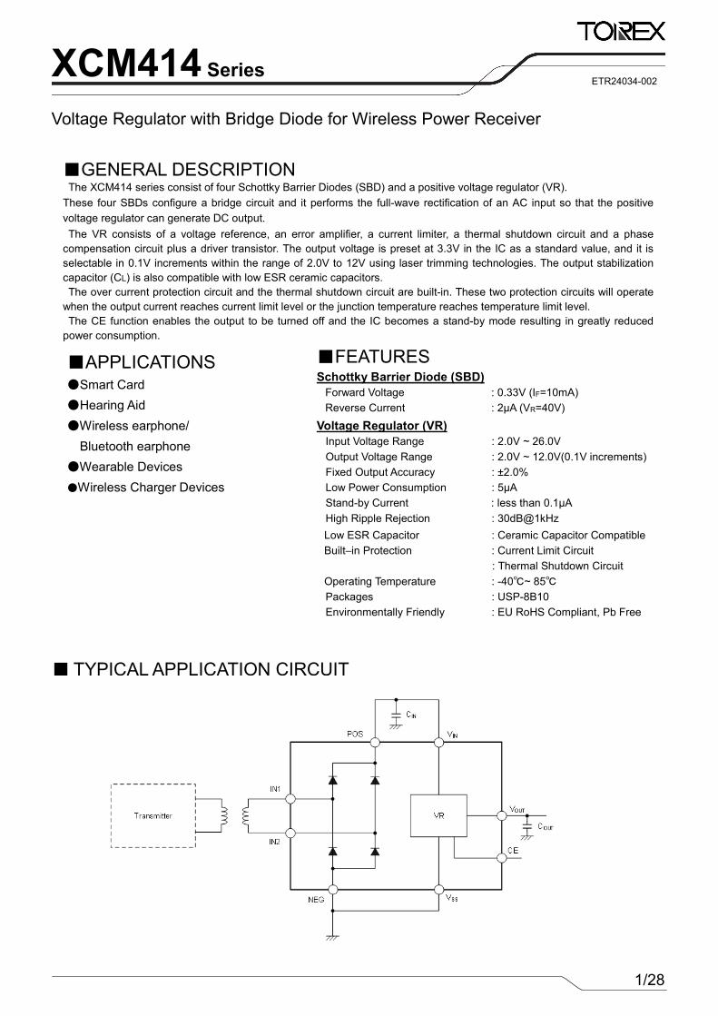
1/28 XCM414 Series Voltage Regulator with Bridge Diode for Wireless Power Receiver ■FEATURES Schottky Barrier Diode (SBD) Forward Voltage : 0.33V (IF=10mA) Reverse Current : 2μA (VR=40V) Voltage Regulator (VR) Input Voltage Range Output Voltage Range : 2.0V ~ 26.0V : 2.0V ~ 12.0V(0.1V increments) Fixed Output Accuracy : ±2.0% Low Power Consumption : 5μA Stand-by Current : less than 0.1μA High Ripple Rejection : 30dB@1kHz Low ESR Capacitor : Ceramic Capacitor Compatible Built–in Protection : Current Limit Circuit : Thermal Shutdown Circuit Operating Temperature : -40℃~ 85℃ Packages : USP-8B10 Environmentally Friendly : EU RoHS Compliant, Pb Free ■GENERAL DESCRIPTION The XCM414 series consist of four Schottky Barrier Diodes (SBD) and a positive voltage regulator (VR). These four SBDs configure a bridge circuit and it performs the full-wave rectification of an AC input so that the positive voltage regulator can generate DC output. The VR consists of a voltage reference, an error amplifier, a current limiter, a thermal shutdown circuit and a phase compensation circuit plus a driver transistor. The output voltage is preset at 3.3V in the IC as a standard value, and it is selectable in 0.1V increments within the range of 2.0V to 12V using laser trimming technologies. The output stabilization capacitor (CL) is also compatible with low ESR ceramic capacitors. The over current protection circuit and the thermal shutdown circuit are built-in. These two protection circuits will operate when the output current reaches current limit level or the junction temperature reaches temperature limit level. The CE function enables the output to be turned off and the IC becomes a stand-by mode resulting in greatly reduced power consumption. ■APPLICATIONS ●Smart Card ●Hearing Aid ●Wireless earphone/ Bluetooth earphone ●Wearable Devices ●Wireless Charger Devices ■ TYPICAL APPLICATION CIRCUIT ETR24034-002
Transcript of n CMOS Low Power Consumption
1/28
XCM414 Series Voltage Regulator with Bridge Diode for Wireless Power Receiver
■FEATURES Schottky Barrier Diode (SBD)
Forward Voltage : 0.33V (IF=10mA) Reverse Current : 2μA (VR=40V)
Voltage Regulator (VR) Input Voltage Range Output Voltage Range
: 2.0V ~ 26.0V : 2.0V ~ 12.0V(0.1V increments)
Fixed Output Accuracy : ±2.0% Low Power Consumption : 5μA Stand-by Current : less than 0.1μA High Ripple Rejection : 30dB@1kHz Low ESR Capacitor : Ceramic Capacitor Compatible Built–in Protection : Current Limit Circuit
: Thermal Shutdown Circuit Operating Temperature : -40℃~ 85℃ Packages : USP-8B10 Environmentally Friendly : EU RoHS Compliant, Pb Free
■GENERAL DESCRIPTION The XCM414 series consist of four Schottky Barrier Diodes (SBD) and a positive voltage regulator (VR).
These four SBDs configure a bridge circuit and it performs the full-wave rectification of an AC input so that the positive voltage regulator can generate DC output. The VR consists of a voltage reference, an error amplifier, a current limiter, a thermal shutdown circuit and a phase
compensation circuit plus a driver transistor. The output voltage is preset at 3.3V in the IC as a standard value, and it is selectable in 0.1V increments within the range of 2.0V to 12V using laser trimming technologies. The output stabilization capacitor (CL) is also compatible with low ESR ceramic capacitors. The over current protection circuit and the thermal shutdown circuit are built-in. These two protection circuits will operate
when the output current reaches current limit level or the junction temperature reaches temperature limit level. The CE function enables the output to be turned off and the IC becomes a stand-by mode resulting in greatly reduced
power consumption.
■APPLICATIONS ●Smart Card ●Hearing Aid ●Wireless earphone/ Bluetooth earphone ●Wearable Devices ●Wireless Charger Devices
■ TYPICAL APPLICATION CIRCUIT
ETR24034-002

2/28
XCM414 Series
PIN NUMBER PIN NAME FUNCTION
USP-8B10
1 IN1 Bridge Input 1
2 POS Bridge Positive
3 VIN Voltage Regulator Input Power
4 VOUT Voltage Regulator Output
5 CE ON/OFF Control (*1)
6 VSS Voltage Regulator Ground
7 IN2 Bridge Input2
8 NEG Bridge Negative
DESIGNATOR DESCRIPTION SYMBOL DESCRIPTION
① TYPE B Fixed
②③④ Output Voltage 020 ~ 120 For the voltage within 2.0V ~ 12.0V (0.1V increments) e.g. 033 ⇒ 3.3V, 105 ⇒ 10.5V
⑤⑥-⑦ Packages Taping Type D2-G USP-8B10 (5,000 pcs/Reel)
PIN NAME DESIGNATOR CONDITIONS IC OPERATION
CE L 0V≦VCE≦0.35V OFF H 1.1V≦VCE≦26.0V ON
OPEN CE=OPEN Undefined state
■PIN CONFIGURATION
■PIN ASSIGNMENT
XCM414①②③④⑤⑥-⑦ (*1)
(*1) The “-G” suffix denotes Halogen and Antimony free as well as being fully EU RoHS compliant.
■ PRODUCT CLASSIFICATION ●Ordering Information
*Please avoid the state of OPEN, and make CE Pin arbitrary fixed potential.
■FUNCTION
* The dissipation pad should be solder-plated in reference to the mount pattern and metal masking so as to enhance mounting strength and heat release. Connect mount pattern D with VSS pin (#6 pin) but don’t connect the mount pattern A, B, and C to other pins, because they are connected with each SBD.
VIN VOUT
VSS
USP-8B10(BOTTOM VIEW)
6 5
4321
8 7
IN1 POS
CEIN2NEG
A B
C
D
(*1) Please avoid the state of OPEN, and make CE Pin arbitrary fixed potential.
3/28
XCM414 Series
PARMETER SYMBOL RATINGS UNITS
● Schottky Barrier Diode (SBD) Repetitive Peak Voltage VRM 40 V
Reverse Voltage (DC) VR 40 V
Forward Current (Average) IF(AV) 200 mA
Peak Forward Surge Current(*1) IFSM 1 A
● Voltage Regulator (VR) (*2) Input Voltage VIN VSS - 0.3 ~ 28 V
Output Voltage VOUT VSS - 0.3 ~ VIN + 0.3 V
CE Input Voltage VCE VSS - 0.3 ~ 28 V
● Common
Power Dissipation (Ta=25℃)
USP-8B10 Pd 1400 (High heat dissipation board) (*3) mW
Operating Ambient Temperature Topr -40 ~ 85 ℃
Storage Temperature Tstg -55 ~ 125 ℃
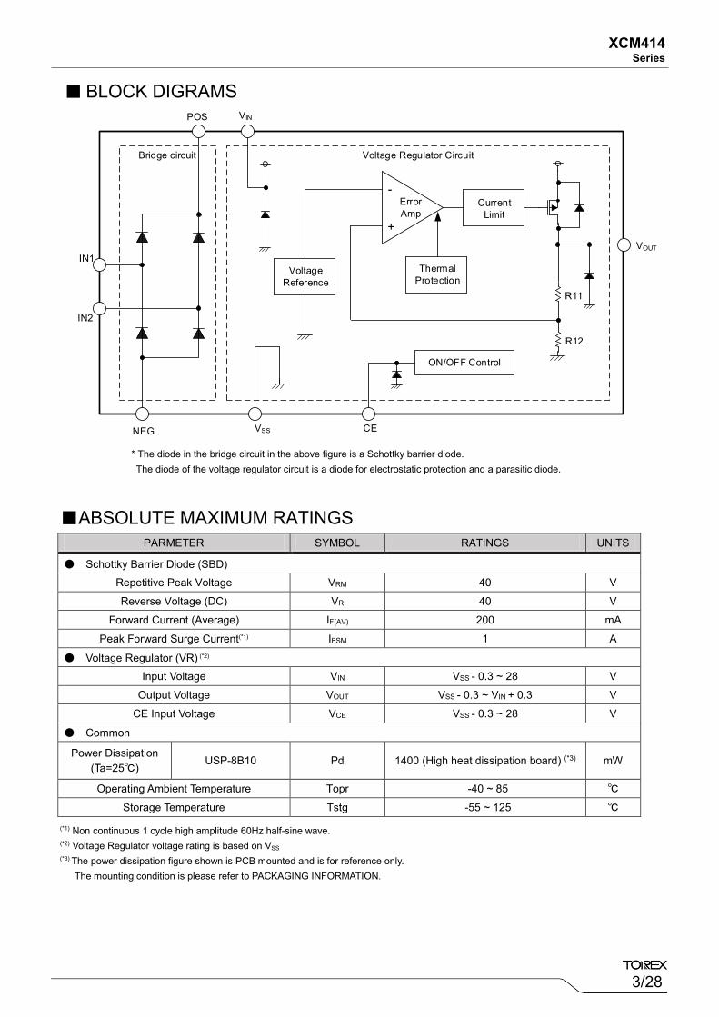
■ BLOCK DIGRAMS
■ABSOLUTE MAXIMUM RATINGS
(*1) Non continuous 1 cycle high amplitude 60Hz half-sine wave. (*2) Voltage Regulator voltage rating is based on VSS (*3) The power dissipation figure shown is PCB mounted and is for reference only. The mounting condition is please refer to PACKAGING INFORMATION.
* The diode in the bridge circuit in the above figure is a Schottky barrier diode. The diode of the voltage regulator circuit is a diode for electrostatic protection and a parasitic diode.
ErrorAmp
CurrentLimit
ThermalProtection
VoltageReference
R11
R12
VIN
VSS
VOUT
+
-
Voltage Regulator Circuit
ON/OFF Control
Bridge circuit
CENEG
POS
IN1
IN2
4/28
XCM414 Series
PARAMETER STMBOL TEST CONDITION MIN. TYP. MAX. UNITS
Forward Voltage VF1 IF=10mA - 0.33 - V VF2 IF=200mA - 0.53 0.6 V
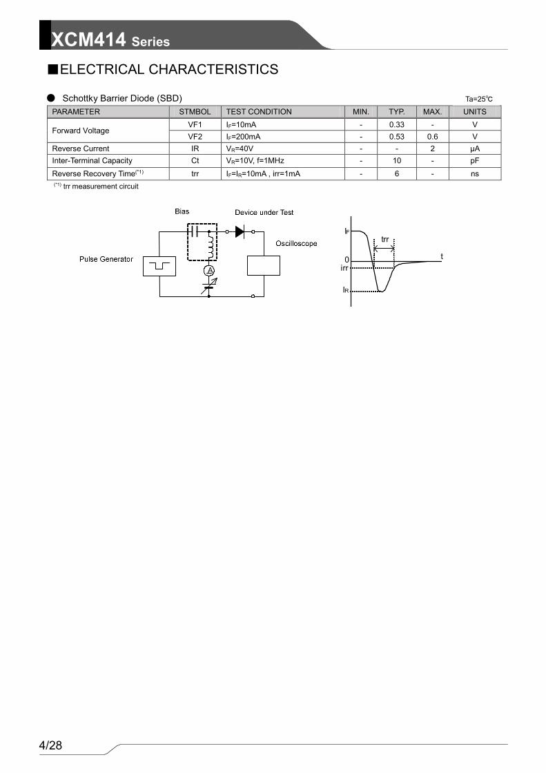
Reverse Current IR VR=40V - - 2 μA Inter-Terminal Capacity Ct VR=10V, f=1MHz - 10 - pF Reverse Recovery Time(*1) trr IF=IR=10mA , irr=1mA - 6 - ns
(*1) trr measurement circuit
■ELECTRICAL CHARACTERISTICS
● Schottky Barrier Diode (SBD)
Ta=25℃
A
IF
IR
trr
tirr0
5/28
XCM414 Series
PARAMETER STMBOL TEST CONDITION MIN. TYP. MAX. UNITS CIRCUIT
Output Voltage VOUT(E) (*2) IOUT=20mA, VCE=VIN E-0 V ①
Maximum Output Current IOUTMAX
VIN= VOUT(T) (*1) +3.0V, VCE=VIN
(VOUT(T)≧3.0V) 150 - - mA ①
VIN=V OUT(T) (*1) +3.0V, VCE=VIN
(VOUT(T)<3.0 V) 100 - - mA ①
Load Regulation △VOUT
1mA≦IOUT≦50mA, VCE=VIN (2.0V≦VOUT(T)
(*1)≦7.0V) - 50 90 mV ①
1mA≦IOUT≦50mA , VCE=VIN ( 7.0V<VOUT(T)
(*1)≦12.0V ) - 110 140 mV ①
Dropout Voltage 1 Vdif1(*3) IOUT=20mA, VCE=VIN - E-1 mV ① Dropout Voltage 2 Vdif2(*3) IOUT=100mA, VCE=VIN - E-2 mV ①
Supply Current ISS VCE=VIN 1 5 9 μA ② Stand-by Current ISTB VCE=VSS - 0.01 0.1 μA ②
Line Regulation 1 △VOUT /
(△VIN・VOUT) VOUT(T)
(*1)+2.0V≦VIN≦26.0V IOUT=5mA, VCE=VIN - 0.05 0.10 %/V ①
Line Regulation 2 △VOUT /
(△VIN・VOUT) VOUT(T)
(*1)+2.0V≦VIN≦26.0V IOUT=13mA, VCE=VIN - 0.15 0.30 %/V ①
Input Voltage VIN 2.0 - 26.0 V -
Output Voltage Temperature Characteristics
△VOUT / (△Topr・V
OUT)
IOUT=20mA , VCE=VIN -40℃≦Topr≦85℃ - ±100 - ppm/℃ ①
Power Supply Rejection Ratio
PSRR VIN=[VOUT(T)
(*1)+2.0]V +0.5Vp-pAC IOUT=20mA, f=1kHz, VCE=VIN
- 30 - dB ③
Short Current ISHORT VCE=VIN - 30 - mA ① CE ”H” Level Voltage VCEH - 1.1 - 26.0 V ① CE ”L” Level Voltage VCEL - 0 - 0.35 V ① CE ”H” Level Current ICEH VIN=VCE=26.0V -0.1 - 0.1 μA ① CE ”L” Level Current ICEL VIN=26.0V, VCE=VSS -0.1 - 0.1 μA ① Thermal Shutdown Detect Temperature
TTSD VCE=VIN Junction Temperature
- 150 - ℃ ①
Thermal Shutdown Release Temperature
TTSR VCE=VIN Junction Temperature
- 125 - ℃ ①
Hysteresis Width TTSD-TTSR VCE=VIN Junction Temperature
- 25 - ℃ -
■ELECTRICAL CHARACTERISTICS (Continued)
● Voltage Regulator (VR)
Ta=25℃
Unless otherwise stated, VIN=VOUT(T)+2.0V. NOTE: *1: VOUT(T): Nominal output voltage *2: VOUT(E): Effective output voltage (i.e. the output voltage when “VOUT(T)+2.0V” is provided at the VIN pin while maintaining a certain IOUT value.) *3: Vdif={VIN1
- VOUT1} VOUT1: VOUT(T)<3.0V, A voltage equal to 98% of the output voltage whenever an amply stabilized IOUT{VOUT(T)+3.0V} is input.
VOUT(T)≧3.0V, A voltage equal to 98% of the output voltage whenever an amply stabilized IOUT{VOUT(T)+2.0V} is input. VIN1: The input voltage when VOUT1 appears as input voltage is gradually decreased.
6/28
XCM414 Series
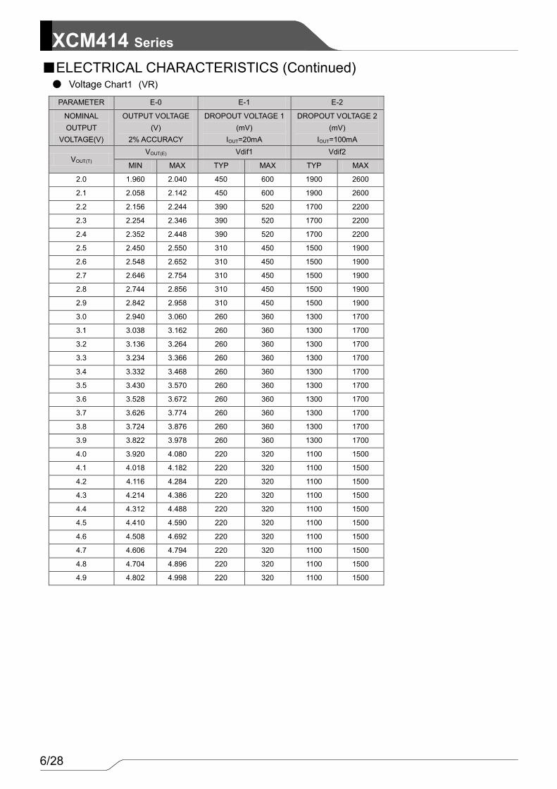
PARAMETER E-0 E-1 E-2
NOMINAL OUTPUT
VOLTAGE(V)
OUTPUT VOLTAGE (V)
2% ACCURACY
DROPOUT VOLTAGE 1 (mV)
IOUT=20mA
DROPOUT VOLTAGE 2 (mV)
IOUT=100mA
VOUT(T) VOUT(E) Vdif1 Vdif2
MIN MAX TYP MAX TYP MAX
2.0 1.960 2.040 450 600 1900 2600
2.1 2.058 2.142 450 600 1900 2600
2.2 2.156 2.244 390 520 1700 2200
2.3 2.254 2.346 390 520 1700 2200
2.4 2.352 2.448 390 520 1700 2200
2.5 2.450 2.550 310 450 1500 1900
2.6 2.548 2.652 310 450 1500 1900
2.7 2.646 2.754 310 450 1500 1900
2.8 2.744 2.856 310 450 1500 1900
2.9 2.842 2.958 310 450 1500 1900
3.0 2.940 3.060 260 360 1300 1700
3.1 3.038 3.162 260 360 1300 1700
3.2 3.136 3.264 260 360 1300 1700
3.3 3.234 3.366 260 360 1300 1700
3.4 3.332 3.468 260 360 1300 1700
3.5 3.430 3.570 260 360 1300 1700
3.6 3.528 3.672 260 360 1300 1700
3.7 3.626 3.774 260 360 1300 1700
3.8 3.724 3.876 260 360 1300 1700
3.9 3.822 3.978 260 360 1300 1700
4.0 3.920 4.080 220 320 1100 1500
4.1 4.018 4.182 220 320 1100 1500
4.2 4.116 4.284 220 320 1100 1500
4.3 4.214 4.386 220 320 1100 1500
4.4 4.312 4.488 220 320 1100 1500
4.5 4.410 4.590 220 320 1100 1500
4.6 4.508 4.692 220 320 1100 1500
4.7 4.606 4.794 220 320 1100 1500
4.8 4.704 4.896 220 320 1100 1500
4.9 4.802 4.998 220 320 1100 1500
● Voltage Chart1 (VR) ■ELECTRICAL CHARACTERISTICS (Continued)
7/28
XCM414 Series
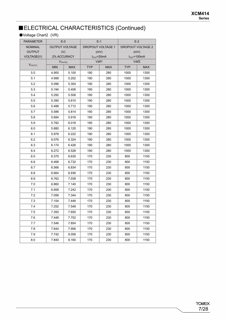
PARAMETER E-0 E-1 E-2
NOMINAL OUTPUT
VOLTAGE(V)
OUTPUT VOLTAGE (V)
2% ACCURACY
DROPOUT VOLTAGE 1 (mV)
IOUT=20mA
DROPOUT VOLTAGE 2 (mV)
IOUT=100mA
VOUT(T) VOUT(E) Vdif1 Vdif2
MIN MAX TYP MAX TYP MAX
5.0 4.900 5.100 190 280 1000 1300
5.1 4.998 5.202 190 280 1000 1300
5.2 5.096 5.304 190 280 1000 1300
5.3 5.194 5.406 190 280 1000 1300
5.4 5.292 5.508 190 280 1000 1300
5.5 5.390 5.610 190 280 1000 1300
5.6 5.488 5.712 190 280 1000 1300
5.7 5.586 5.814 190 280 1000 1300
5.8 5.684 5.916 190 280 1000 1300
5.9 5.782 6.018 190 280 1000 1300
6.0 5.880 6.120 190 280 1000 1300
6.1 5.978 6.222 190 280 1000 1300
6.2 6.076 6.324 190 280 1000 1300
6.3 6.174 6.426 190 280 1000 1300
6.4 6.272 6.528 190 280 1000 1300
6.5 6.370 6.630 170 230 800 1150
6.6 6.468 6.732 170 230 800 1150
6.7 6.566 6.834 170 230 800 1150
6.8 6.664 6.936 170 230 800 1150
6.9 6.762 7.038 170 230 800 1150
7.0 6.860 7.140 170 230 800 1150
7.1 6.958 7.242 170 230 800 1150
7.2 7.056 7.344 170 230 800 1150
7.3 7.154 7.446 170 230 800 1150
7.4 7.252 7.548 170 230 800 1150
7.5 7.350 7.650 170 230 800 1150
7.6 7.448 7.752 170 230 800 1150
7.7 7.546 7.854 170 230 800 1150
7.8 7.644 7.956 170 230 800 1150
7.9 7.742 8.058 170 230 800 1150
8.0 7.840 8.160 170 230 800 1150
■ELECTRICAL CHARACTERISTICS (Continued) ●Voltage Chart2 (VR)
8/28
XCM414 Series
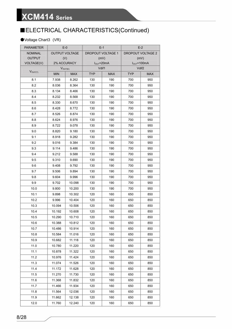
PARAMETER E-0 E-1 E-2
NOMINAL OUTPUT
VOLTAGE(V)
OUTPUT VOLTAGE (V)
2% ACCURACY
DROPOUT VOLTAGE 1 (mV)
IOUT=20mA
DROPOUT VOLTAGE 2 (mV)
IOUT=100mA
VOUT(T) VOUT(E) Vdif1 Vdif2
MIN MAX TYP MAX TYP MAX
8.1 7.938 8.262 130 190 700 950
8.2 8.036 8.364 130 190 700 950
8.3 8.134 8.466 130 190 700 950
8.4 8.232 8.568 130 190 700 950
8.5 8.330 8.670 130 190 700 950
8.6 8.428 8.772 130 190 700 950
8.7 8.526 8.874 130 190 700 950
8.8 8.624 8.976 130 190 700 950
8.9 8.722 9.078 130 190 700 950
9.0 8.820 9.180 130 190 700 950
9.1 8.918 9.282 130 190 700 950
9.2 9.016 9.384 130 190 700 950
9.3 9.114 9.486 130 190 700 950
9.4 9.212 9.588 130 190 700 950
9.5 9.310 9.690 130 190 700 950
9.6 9.408 9.792 130 190 700 950
9.7 9.506 9.894 130 190 700 950
9.8 9.604 9.996 130 190 700 950
9.9 9.702 10.098 130 190 700 950
10.0 9.800 10.200 130 190 700 950
10.1 9.898 10.302 120 160 650 850
10.2 9.996 10.404 120 160 650 850
10.3 10.094 10.506 120 160 650 850
10.4 10.192 10.608 120 160 650 850
10.5 10.290 10.710 120 160 650 850
10.6 10.388 10.812 120 160 650 850
10.7 10.486 10.914 120 160 650 850
10.8 10.584 11.016 120 160 650 850
10.9 10.682 11.118 120 160 650 850
11.0 10.780 11.220 120 160 650 850
11.1 10.878 11.322 120 160 650 850
11.2 10.976 11.424 120 160 650 850
11.3 11.074 11.526 120 160 650 850
11.4 11.172 11.628 120 160 650 850
11.5 11.270 11.730 120 160 650 850
11.6 11.368 11.832 120 160 650 850
11.7 11.466 11.934 120 160 650 850
11.8 11.564 12.036 120 160 650 850
11.9 11.662 12.138 120 160 650 850
12.0 11.760 12.240 120 160 650 850
●Voltage Chart3 (VR)
■ELECTRICAL CHARACTERISTICS(Continued)
9/28
XCM414 Series
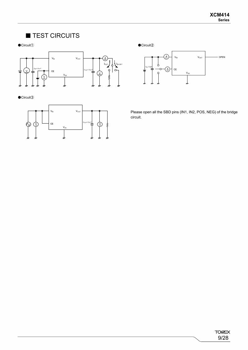
●Circuit① ●Circuit② ●Circuit③
■ TEST CIRCUITS VIN
VSS
CE
VOUT
A
OPENA
CIN=1.0uF
VIN
VSS
CE
VOUT
V
VV
A
IOUT ISH OR T
CIN=1.0μFCOUT=1.0μF
VIN
VSS
CE
VOUT
V~
V~
COUT=1.0μF
Please open all the SBD pins (IN1, IN2, POS, NEG) of the bridge circuit.
10/28
XCM414 Series
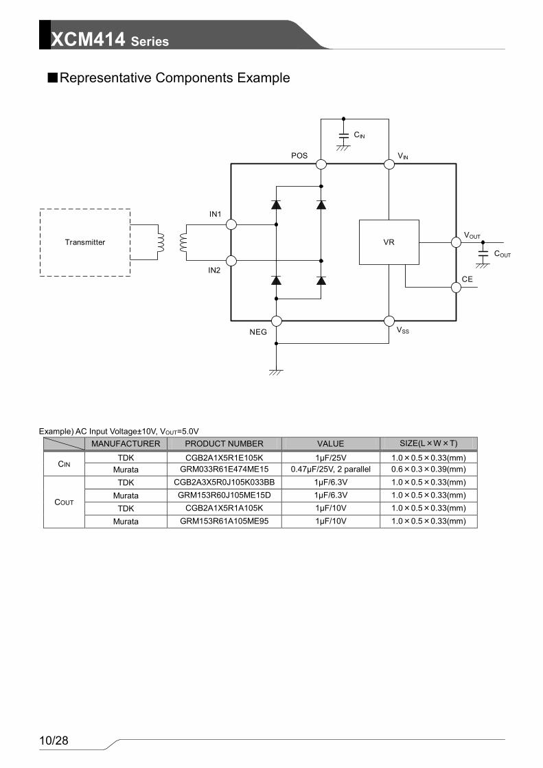
Example) AC Input Voltage±10V, VOUT=5.0V
MANUFACTURER PRODUCT NUMBER VALUE SIZE(L×W×T)
CIN TDK CGB2A1X5R1E105K 1μF/25V 1.0×0.5×0.33(mm)
Murata GRM033R61E474ME15 0.47μF/25V, 2 parallel 0.6×0.3×0.39(mm)
COUT
TDK CGB2A3X5R0J105K033BB 1μF/6.3V 1.0×0.5×0.33(mm) Murata GRM153R60J105ME15D 1μF/6.3V 1.0×0.5×0.33(mm)
TDK CGB2A1X5R1A105K 1μF/10V 1.0×0.5×0.33(mm) Murata GRM153R61A105ME95 1μF/10V 1.0×0.5×0.33(mm)
■Representative Components Example
VRTransmitter
IN1
IN2
NEG VSS
POS VIN
VOUT
CE
COUT
CIN
11/28
XCM414 Series
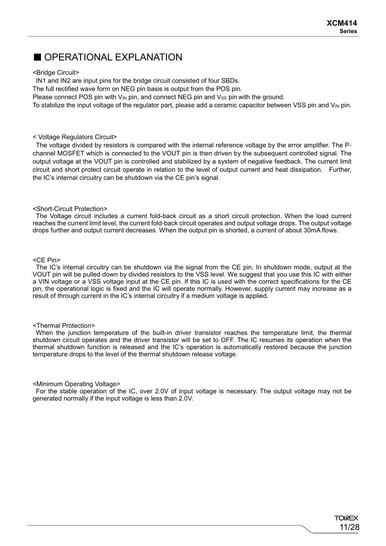
<Bridge Circuit> IN1 and IN2 are input pins for the bridge circuit consisted of four SBDs.
The full rectified wave form on NEG pin basis is output from the POS pin. Please connect POS pin with VIN pin, and connect NEG pin and VSS pin with the ground. To stabilize the input voltage of the regulator part, please add a ceramic capacitor between VSS pin and VIN pin.
< Voltage Regulators Circuit> The voltage divided by resistors is compared with the internal reference voltage by the error amplifier. The P-
channel MOSFET which is connected to the VOUT pin is then driven by the subsequent controlled signal. The output voltage at the VOUT pin is controlled and stabilized by a system of negative feedback. The current limit circuit and short protect circuit operate in relation to the level of output current and heat dissipation. Further, the IC’s internal circuitry can be shutdown via the CE pin’s signal.
<Short-Circuit Protection> The Voltage circuit includes a current fold-back circuit as a short circuit protection. When the load current
reaches the current limit level, the current fold-back circuit operates and output voltage drops. The output voltage drops further and output current decreases. When the output pin is shorted, a current of about 30mA flows.
<CE Pin> The IC’s internal circuitry can be shutdown via the signal from the CE pin. In shutdown mode, output at the
VOUT pin will be pulled down by divided resistors to the VSS level. We suggest that you use this IC with either a VIN voltage or a VSS voltage input at the CE pin. If this IC is used with the correct specifications for the CE pin, the operational logic is fixed and the IC will operate normally. However, supply current may increase as a result of through current in the IC’s internal circuitry if a medium voltage is applied.
<Thermal Protection> When the junction temperature of the built-in driver transistor reaches the temperature limit, the thermal
shutdown circuit operates and the driver transistor will be set to OFF. The IC resumes its operation when the thermal shutdown function is released and the IC’s operation is automatically restored because the junction temperature drops to the level of the thermal shutdown release voltage.
<Minimum Operating Voltage> For the stable operation of the IC, over 2.0V of input voltage is necessary. The output voltage may not be
generated normally if the input voltage is less than 2.0V.
■ OPERATIONAL EXPLANATION
12/28
XCM414 Series
■ NOTES ON USE
1. Please use this IC within the stated absolute maximum ratings. The IC is liable to malfunction should the ratings be exceeded.
2. Where wiring impedance is high, operations may become unstable due to the noise and/or phase lag depending on output current. Please strengthen VIN and VSS wiring in particular.
3. Since the absolute maximum rated voltage of the Schottky Barrier Diode is 40V, the AC input voltage input to the IN 1 terminal and IN 2 terminal should not exceed ± 20V.
4. In order to smooth the full-wave rectified output by the bridge circuit and stabilize the input of the voltage regulator, an input capacitor CIN of about 1.0μF is required between the power supply input pin (VIN) and the ground pin (VSS). When increasing the capacitance value, select the input capacitor (CIN) so that the inrush current at power-on will not exceed the peak forward surge current 1A of the Schottky Barrier Diode. In addition, it is necessary to connect the NEG terminal of the bridge circuit and the ground terminal (VSS) of the voltage regulator circuit.
5. The output voltage fluctuation such as under shoot or over shoot, which occurs because of the load change can be controlled by placing the output capacitor COUT around 0.1μF~1.0μF between the VOUT pin and VSS pin. The input capacitor (CIN) and the output capacitor (COUT) should be placed to the IC as close as possible with a shorter wiring.
6. Torex places an importance on improving our products and their reliability. We request that users incorporate fail-safe designs and post-aging protection treatment when using Torex products in their systems.
13/28
XCM414 Series
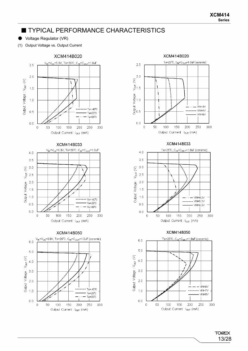
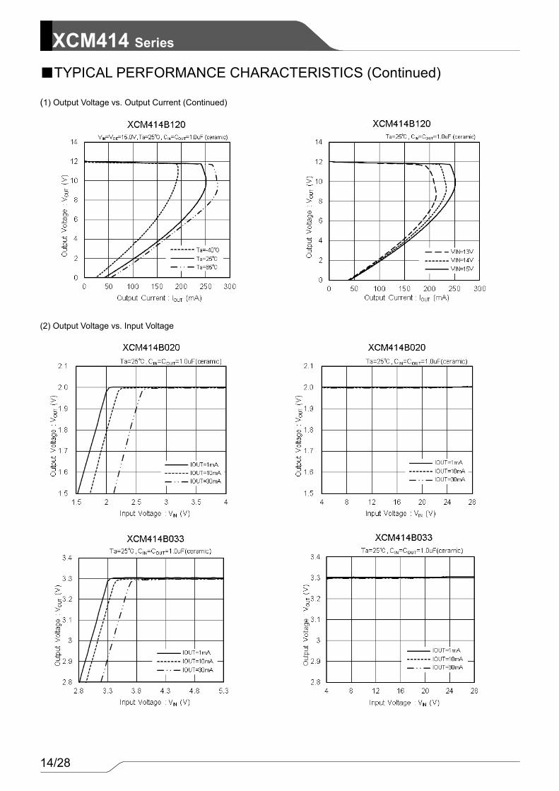
(1) Output Voltage vs. Output Current
■ TYPICAL PERFORMANCE CHARACTERISTICS
● Voltage Regulator (VR)
14/28
XCM414 Series ■TYPICAL PERFORMANCE CHARACTERISTICS (Continued) (1) Output Voltage vs. Output Current (Continued)
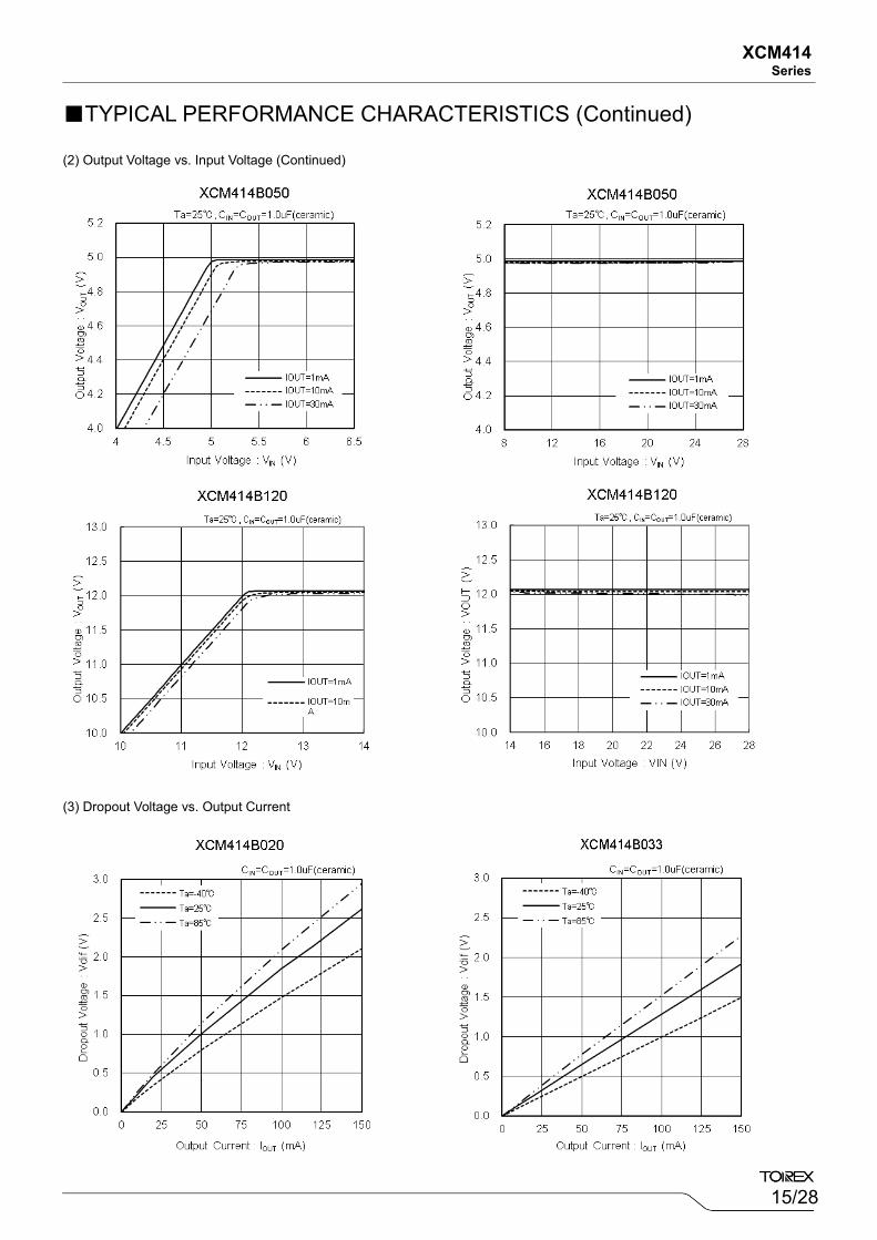
(2) Output Voltage vs. Input Voltage
15/28
XCM414 Series
■TYPICAL PERFORMANCE CHARACTERISTICS (Continued) (2) Output Voltage vs. Input Voltage (Continued)
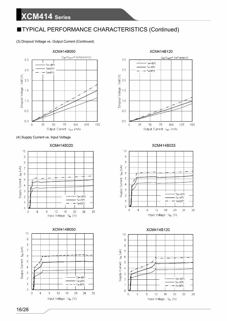
(3) Dropout Voltage vs. Output Current
16/28
XCM414 Series ■TYPICAL PERFORMANCE CHARACTERISTICS (Continued) (3) Dropout Voltage vs. Output Current (Continued)
(4) Supply Current vs. Input Voltage
17/28
XCM414 Series
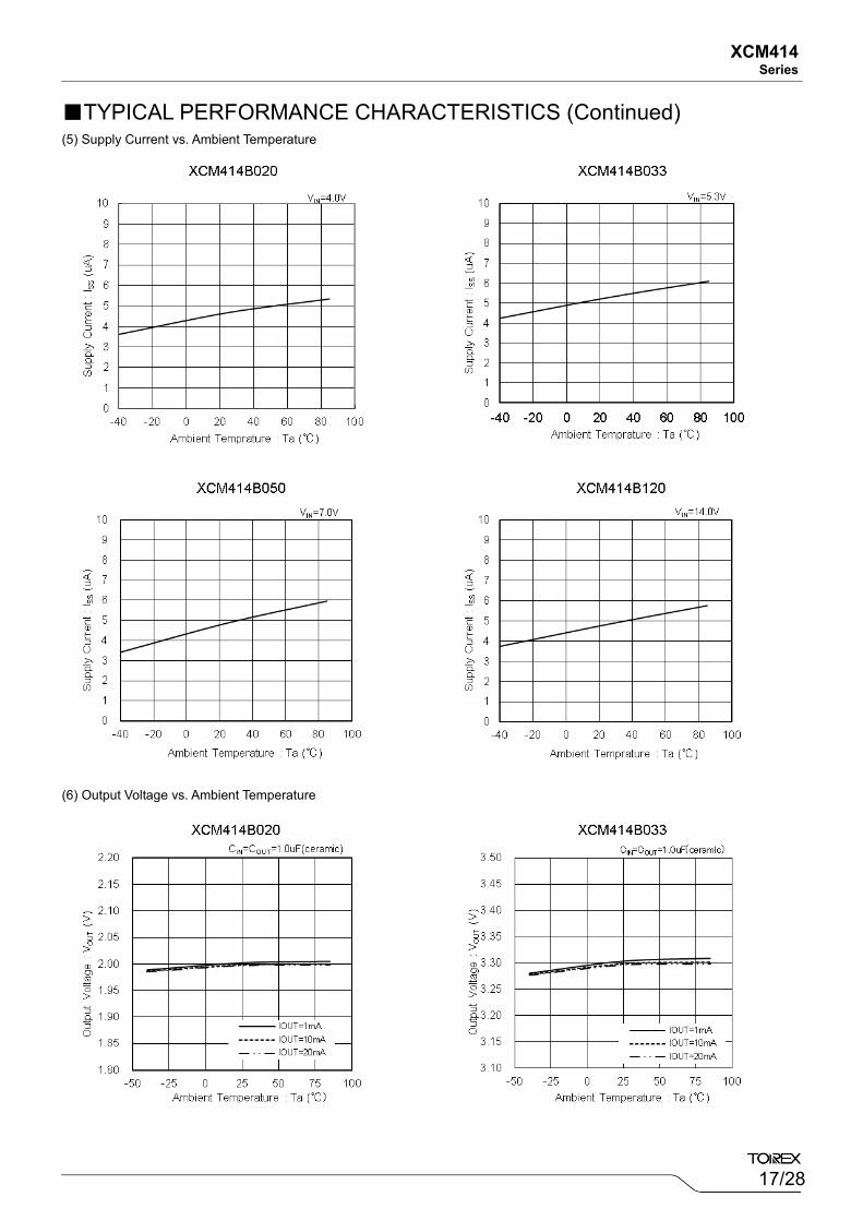
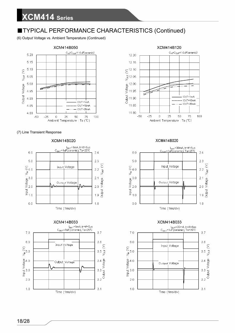
■TYPICAL PERFORMANCE CHARACTERISTICS (Continued) (5) Supply Current vs. Ambient Temperature
(6) Output Voltage vs. Ambient Temperature
18/28
XCM414 Series ■TYPICAL PERFORMANCE CHARACTERISTICS (Continued) (6) Output Voltage vs. Ambient Temperature (Continued)
(7) Line Transient Response
19/28
XCM414 Series
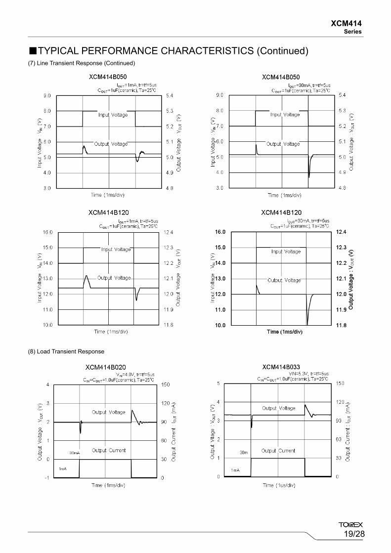
■TYPICAL PERFORMANCE CHARACTERISTICS (Continued) (7) Line Transient Response (Continued)
(8) Load Transient Response
20/28
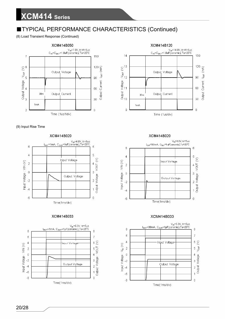
XCM414 Series ■TYPICAL PERFORMANCE CHARACTERISTICS (Continued) (8) Load Transient Response (Continued)
(9) Input Rise Time
21/28
XCM414 Series
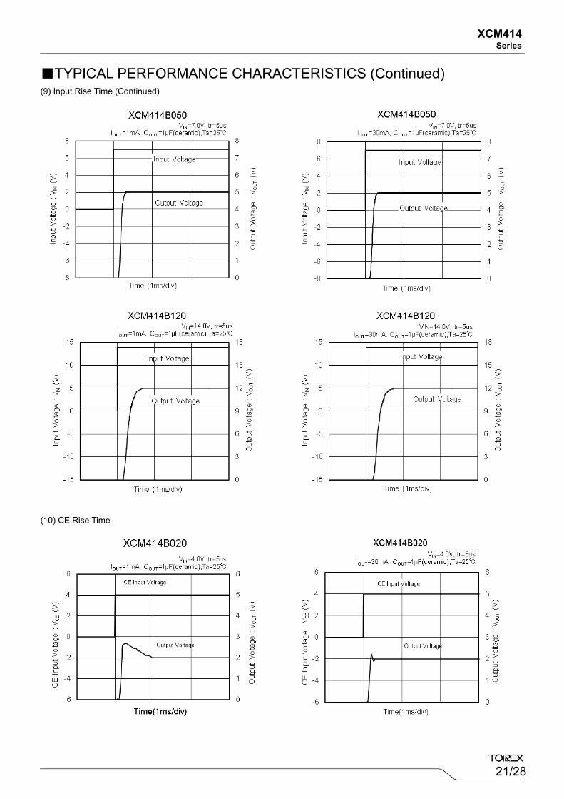
■TYPICAL PERFORMANCE CHARACTERISTICS (Continued) (9) Input Rise Time (Continued)
(10) CE Rise Time
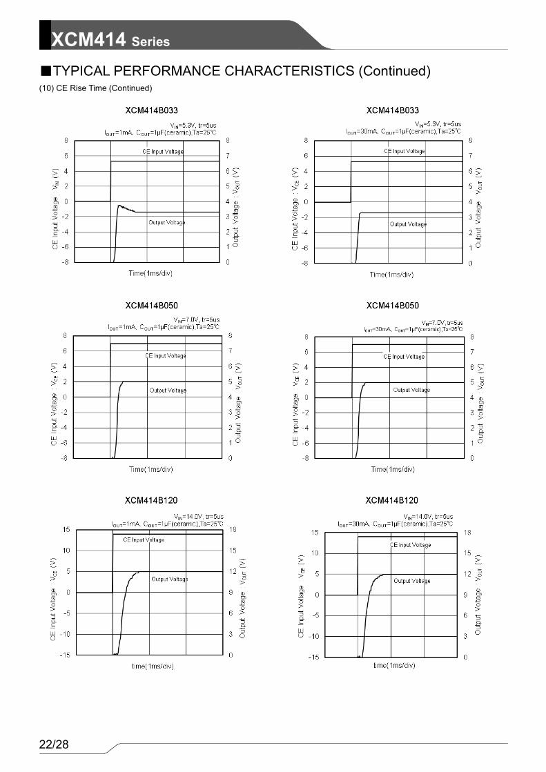
22/28
XCM414 Series ■TYPICAL PERFORMANCE CHARACTERISTICS (Continued) (10) CE Rise Time (Continued)
23/28
XCM414 Series
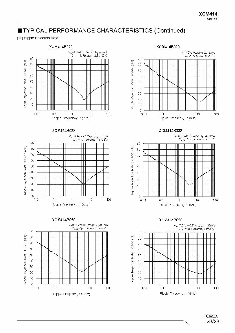
■TYPICAL PERFORMANCE CHARACTERISTICS (Continued) (11) Ripple Rejection Rate
24/28
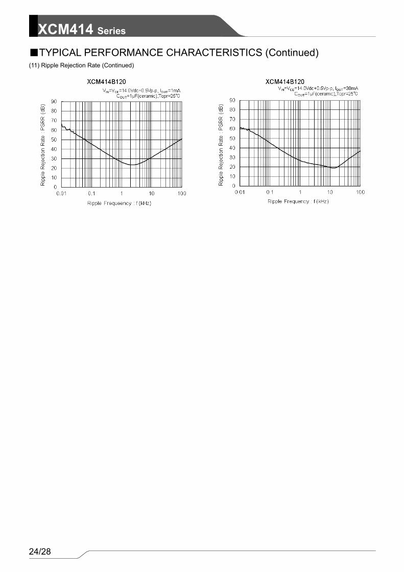
XCM414 Series ■TYPICAL PERFORMANCE CHARACTERISTICS (Continued) (11) Ripple Rejection Rate (Continued)
25/28
XCM414 Series
■TYPICAL PERFORMANCE CHARACTERISTICS (Continued)
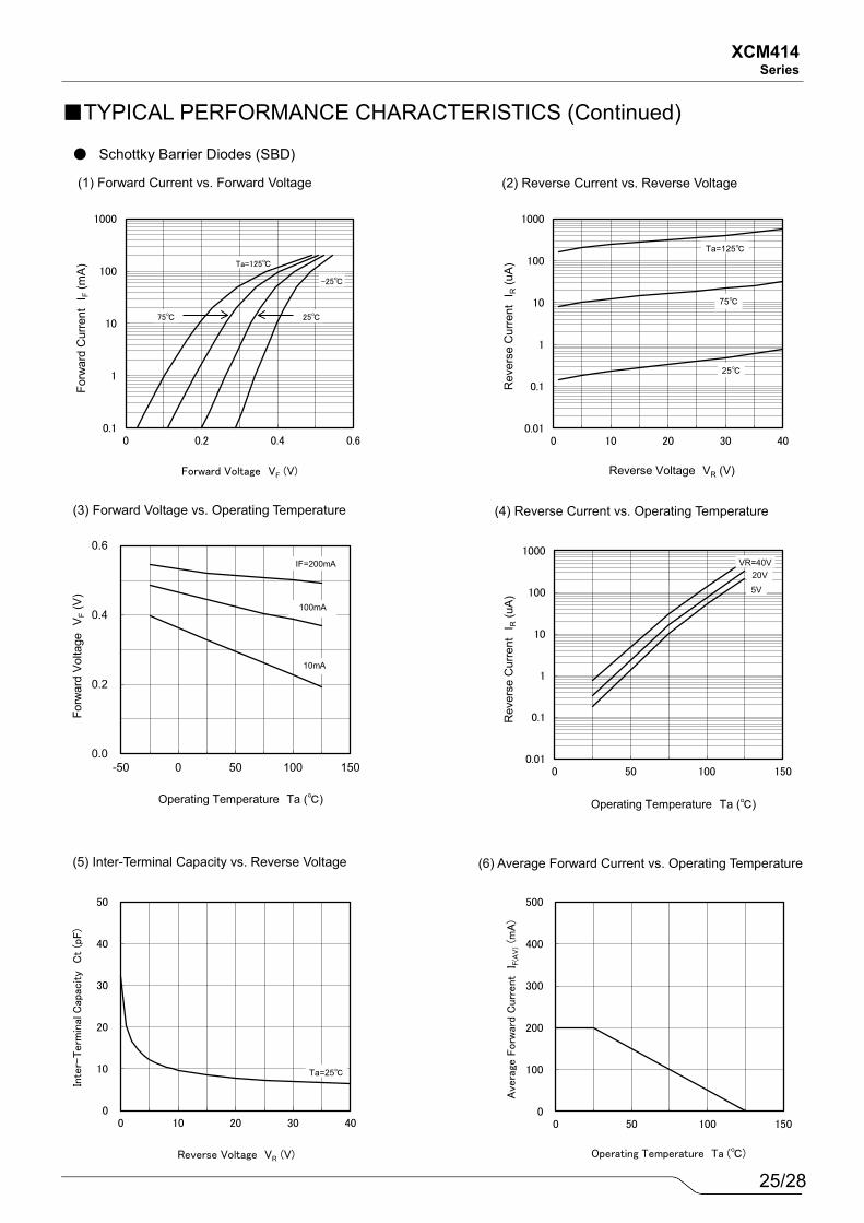
(1) Forward Current vs. Forward Voltage (2) Reverse Current vs. Reverse Voltage
(3) Forward Voltage vs. Operating Temperature (4) Reverse Current vs. Operating Temperature
(5) Inter-Terminal Capacity vs. Reverse Voltage (6) Average Forward Current vs. Operating Temperature
● Schottky Barrier Diodes (SBD)
0.1
1
10
100
1000
0 0.2 0.4 0.6
Forw
ard
Cur
rent
I F(m
A)
Forward Voltage VF (V)
Ta=125℃
-25℃
25℃75℃
0.01
0.1
1
10
100
1000
0 10 20 30 40
Rev
erse
Cur
rent
I R(u
A)
Reverse Voltage VR (V)
Ta=125℃
25℃
75℃
0.01
0.1
1
10
100
1000
0 50 100 150
Rev
erse
Cur
rent
I R(u
A)
Operating Temperature Ta (℃)
VR=40V20V5V
0.0
0.2
0.4
0.6
-50 0 50 100 150
Forw
ard
Volta
geV F
(V)
Operating Temperature Ta (℃)
IF=200mA
100mA
10mA
0
100
200
300
400
500
0 50 100 150
Ave
rage
Forw
ard
Curr
ent
I F(A
V)(m
A)
Operating Temperature Ta (℃)
0
10
20
30
40
50
0 10 20 30 40
Inte
r-Term
inal
Cap
acity
Ct
(pF)
Reverse Voltage VR (V)
Ta=25℃
26/28
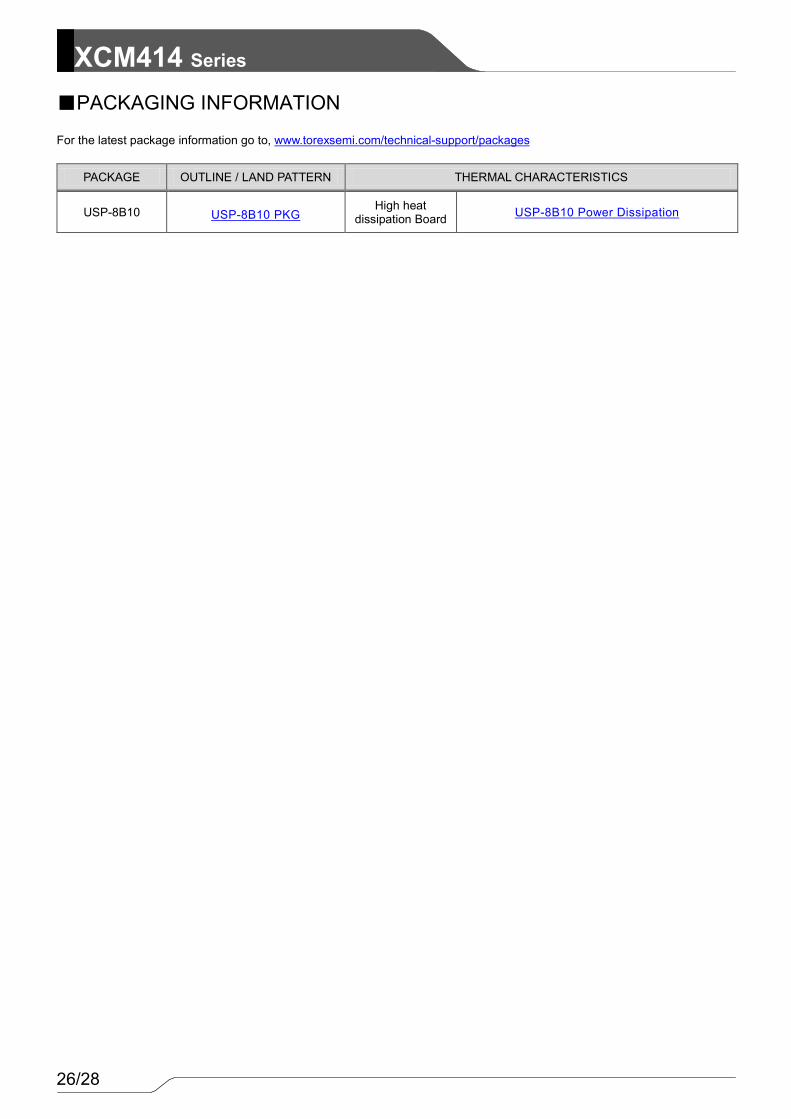
XCM414 Series ■PACKAGING INFORMATION
For the latest package information go to, www.torexsemi.com/technical-support/packages
PACKAGE OUTLINE / LAND PATTERN THERMAL CHARACTERISTICS
USP-8B10 USP-8B10 PKG High heat
dissipation Board USP-8B10 Power Dissipation
27/28
XCM414 Series
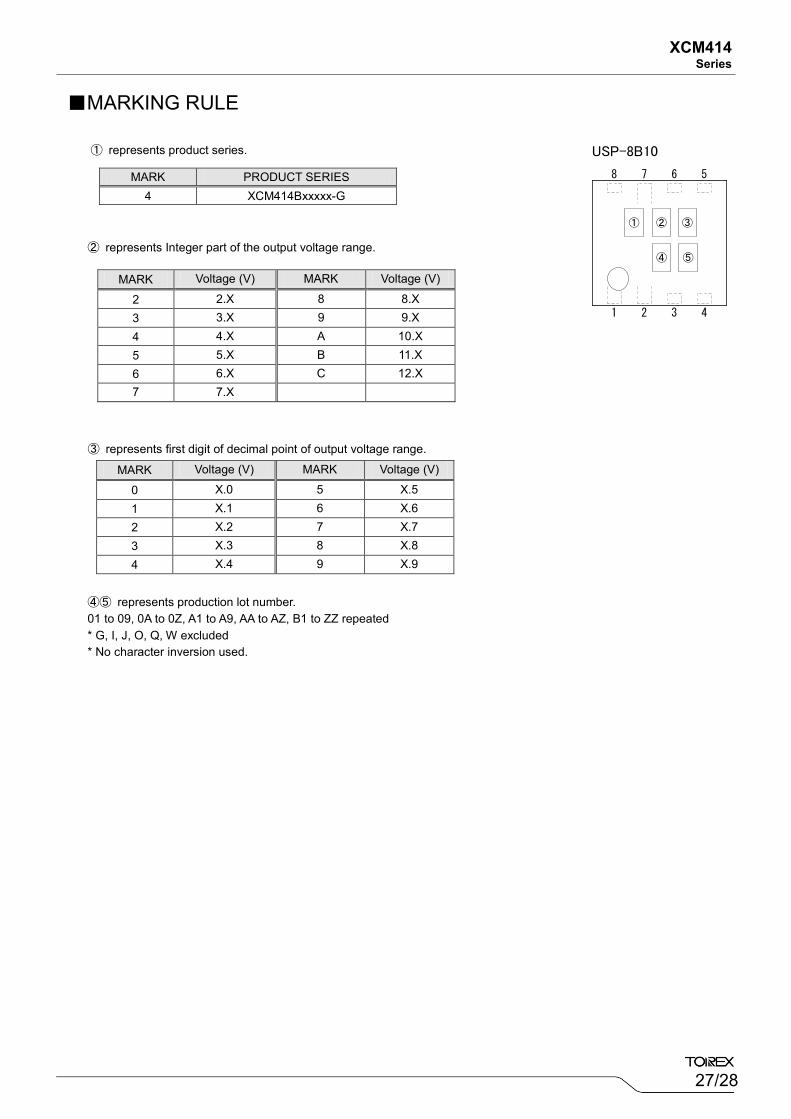
MARK Voltage (V) MARK Voltage (V)
2 2.X 8 8.X 3 3.X 9 9.X 4 4.X A 10.X 5 5.X B 11.X 6 6.X C 12.X 7 7.X
MARK PRODUCT SERIES 4 XCM414Bxxxxx-G
■MARKING RULE
USP-8B10
3 4
5678
1 2
① ② ③
④ ⑤
① represents product series.
② represents Integer part of the output voltage range.
③ represents first digit of decimal point of output voltage range.
MARK Voltage (V) MARK Voltage (V)
0 X.0 5 X.5 1 X.1 6 X.6 2 X.2 7 X.7 3 X.3 8 X.8 4 X.4 9 X.9
④⑤ represents production lot number. 01 to 09, 0A to 0Z, A1 to A9, AA to AZ, B1 to ZZ repeated * G, I, J, O, Q, W excluded * No character inversion used.
28/28
XCM414 Series
1. The product and product specifications contained herein are subject to change without notice to improve performance characteristics. Consult us, or our representatives before use, to confirm that the information in this datasheet is up to date.
2. The information in this datasheet is intended to illustrate the operation and characteristics of our
products. We neither make warranties or representations with respect to the accuracy or completeness of the information contained in this datasheet nor grant any license to any intellectual property rights of ours or any third party concerning with the information in this datasheet.
3. Applicable export control laws and regulations should be complied and the procedures required by
such laws and regulations should also be followed, when the product or any information contained in this datasheet is exported.
4. The product is neither intended nor warranted for use in equipment of systems which require extremely
high levels of quality and/or reliability and/or a malfunction or failure which may cause loss of human life, bodily injury, serious property damage including but not limited to devices or equipment used in 1) nuclear facilities, 2) aerospace industry, 3) medical facilities, 4) automobile industry and other transportation industry and 5) safety devices and safety equipment to control combustions and explosions. Do not use the product for the above use unless agreed by us in writing in advance.
5. Although we make continuous efforts to improve the quality and reliability of our products; nevertheless
Semiconductors are likely to fail with a certain probability. So in order to prevent personal injury and/or property damage resulting from such failure, customers are required to incorporate adequate safety measures in their designs, such as system fail safes, redundancy and fire prevention features.
6. Our products are not designed to be Radiation-resistant.
7. Please use the product listed in this datasheet within the specified ranges.
8. We assume no responsibility for damage or loss due to abnormal use.
9. All rights reserved. No part of this datasheet may be copied or reproduced unless agreed by Torex
Semiconductor Ltd in writing in advance.
TOREX SEMICONDUCTOR LTD.