
DesignofaVersatileandLowCost μVolt ...researchbank.rmit.edu.au/view/rmit:8355/n2006008507.pdfif...
6
Hindawi Publishing Corporation EURASIP Journal on Advances in Signal Processing Volume 2008, Article ID 370171, 6 pages doi:10.1155/2008/370171 Research Article Design of a Versatile and Low Cost μVolt Level A to D Conversion System for Use in Medical Instrumentation Applications Kerry Williams and Neil Robinson School of Applied Sciences, RMIT University, Melbourne, Victoria 3000, Australia Correspondence should be addressed to Kerry Williams, [email protected] Received 27 November 2007; Revised 3 April 2008; Accepted 14 August 2008 Recommended by P.-C. Chung Modern medical facilities place considerable reliance on electronic instrumentation for purposes of calibration and monitoring of therapeutic processes, many of which employ electrical and electronic apparatus that itself generates considerable levels of interference in the form of background electromagnetic radiation (EMR). Additionally diverse ambient conditions in the clinical environment such as uncontrolled temperature, humidity, noise, and vibration place added stress on sensitive instrumentation. In order to obtain accurate, repeatable, and reliable data in such environments, instrumentation used must be largely immune to these factors. Analogue instrumentation is particularly susceptible to unstable environmental conditions. Sensors typically output an analogue current or voltage and it can be demonstrated that considerable overall benefit to the measuring process would result if sensor outputs could be converted to a robust digital format at the earliest possible stage. A practical and low cost system for A to D conversion at μVolt signal levels is described in this work. It has been successfully employed in portable radiation dosimetry instrumentation and used under diverse clinical conditions and it affords an improvement in signal resolution in excess of an order of magnitude over commonly used analogue techniques. Copyright © 2008 K. Williams and N. Robinson. This is an open access article distributed under the Creative Commons Attribution License, which permits unrestricted use, distribution, and reproduction in any medium, provided the original work is properly cited. 1. INTRODUCTION Development of the instrument described in this paper was inspired by a requirement in our laboratories to measure X-ray fields using near tissue equivalent plastic organic scintillator materials as the sensor element. Under clinical conditions where beam energies in the KVp range are used, these sensors produce extremely low levels of light which when interfaced with the most sensitive of photodiodes yet only produce output currents in the nanoamp region. When coupled with a well shielded buffer amplifier, this arrangement still only provides usable output levels of a few microvolts. The task of raising such signal levels to a point where adequate resolution could be achieved, plus the potential to capture and store the data, presented particular difficulties. Laboratory systems operated in a controlled environment can be effective for the measurement of medium to high level signals but may lack stability and resolution when very low signal levels are encountered [1] and are generally costly and lack portability. Our research has resulted in the design and development of a practical and portable instrument which has been effectively applied in clinical dosimetry situations involving near tissue equivalent radiation dose measurements [2, 3]. Technical details outlining the practical implementation of the system are given below. Analogue circuitry is readily affected by changes in ambient temperature, vibration, unexpected variations in power supply voltages, and the like. In many instances, interference levels from these sources and extraneous EMR generated by adjacent clinical equipment such as X-ray generators, linear accelerators, and general control and computing devices can readily exceed wanted signal levels by several orders of magnitude. The ability to achieve reliable very low level analogue amplification in anything but controlled laboratory con- ditions presents a considerable challenge, and without a guaranteed level of performance and stability in front end
-
Upload
truongngoc -
Category
Documents
-
view
221 -
download
0
Transcript of DesignofaVersatileandLowCost μVolt ...researchbank.rmit.edu.au/view/rmit:8355/n2006008507.pdfif...
Hindawi Publishing CorporationEURASIP Journal on Advances in Signal ProcessingVolume 2008, Article ID 370171, 6 pagesdoi:10.1155/2008/370171
Research ArticleDesign of a Versatile and Low Cost μVoltLevel A to D Conversion System for Use inMedical Instrumentation Applications
Kerry Williams and Neil Robinson
School of Applied Sciences, RMIT University, Melbourne, Victoria 3000, Australia
Correspondence should be addressed to Kerry Williams, [email protected]
Received 27 November 2007; Revised 3 April 2008; Accepted 14 August 2008
Recommended by P.-C. Chung
Modern medical facilities place considerable reliance on electronic instrumentation for purposes of calibration and monitoringof therapeutic processes, many of which employ electrical and electronic apparatus that itself generates considerable levels ofinterference in the form of background electromagnetic radiation (EMR). Additionally diverse ambient conditions in the clinicalenvironment such as uncontrolled temperature, humidity, noise, and vibration place added stress on sensitive instrumentation.In order to obtain accurate, repeatable, and reliable data in such environments, instrumentation used must be largely immune tothese factors. Analogue instrumentation is particularly susceptible to unstable environmental conditions. Sensors typically outputan analogue current or voltage and it can be demonstrated that considerable overall benefit to the measuring process would resultif sensor outputs could be converted to a robust digital format at the earliest possible stage. A practical and low cost system for Ato D conversion at μVolt signal levels is described in this work. It has been successfully employed in portable radiation dosimetryinstrumentation and used under diverse clinical conditions and it affords an improvement in signal resolution in excess of an orderof magnitude over commonly used analogue techniques.
Copyright © 2008 K. Williams and N. Robinson. This is an open access article distributed under the Creative CommonsAttribution License, which permits unrestricted use, distribution, and reproduction in any medium, provided the original work isproperly cited.
1. INTRODUCTION
Development of the instrument described in this paper wasinspired by a requirement in our laboratories to measureX-ray fields using near tissue equivalent plastic organicscintillator materials as the sensor element. Under clinicalconditions where beam energies in the KVp range are used,these sensors produce extremely low levels of light whichwhen interfaced with the most sensitive of photodiodes yetonly produce output currents in the nanoamp region.
When coupled with a well shielded buffer amplifier,this arrangement still only provides usable output levelsof a few microvolts. The task of raising such signal levelsto a point where adequate resolution could be achieved,plus the potential to capture and store the data, presentedparticular difficulties. Laboratory systems operated in acontrolled environment can be effective for the measurementof medium to high level signals but may lack stabilityand resolution when very low signal levels are encountered
[1] and are generally costly and lack portability. Ourresearch has resulted in the design and development of apractical and portable instrument which has been effectivelyapplied in clinical dosimetry situations involving near tissueequivalent radiation dose measurements [2, 3]. Technicaldetails outlining the practical implementation of the systemare given below.
Analogue circuitry is readily affected by changes inambient temperature, vibration, unexpected variations inpower supply voltages, and the like. In many instances,interference levels from these sources and extraneous EMRgenerated by adjacent clinical equipment such as X-raygenerators, linear accelerators, and general control andcomputing devices can readily exceed wanted signal levels byseveral orders of magnitude.
The ability to achieve reliable very low level analogueamplification in anything but controlled laboratory con-ditions presents a considerable challenge, and without aguaranteed level of performance and stability in front end
E72964
Typewritten Text
E72964
Typewritten Text
E72964
Typewritten Text
Citation: Williams, K and Robinson, N 2008, 'Design of a versatile and low cost microvolt level A to D conversion system for use in medical instrumentation applications', Eurasip Journal on Advances in Signal Processing, vol. 2008, pp. 1-6.
E72964
Typewritten Text
E72964
Typewritten Text
2 EURASIP Journal on Advances in Signal Processing
Calibrationfactor
Bias currentgenerator
Sensingdevice
Bufferamplifier
Current tofrequencyconverter
Linedriver
Readoutdevice orcomputer
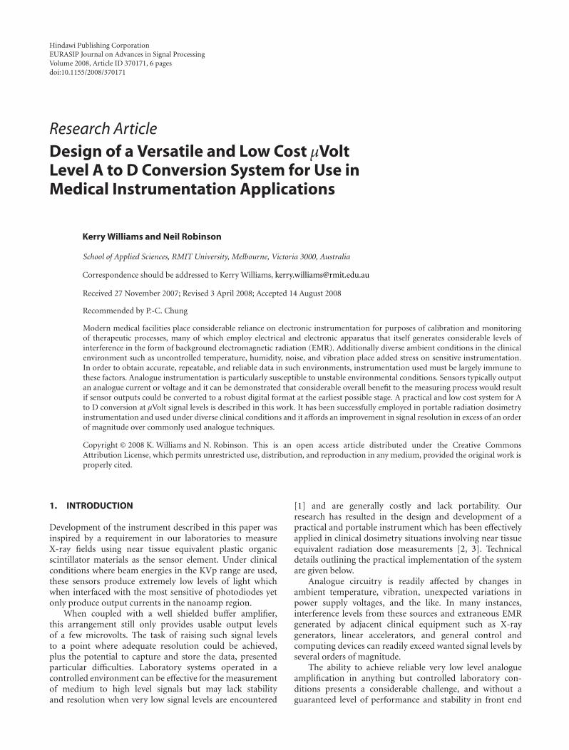
Figure 1: Block diagram showing overview of concept and signal processing chain.
21
123
4
123
4
123
4
8
3
1
23
45
MC33464
LMV751MAX4122
1N4148
LMV751
Select
Hold
ZRB 500
PIN 5
BC549B
Reset
C3
R3
U1
D1
C2
C1
C5
R6
U4
8
8 LTC 1799
R1
R2
R9
U3C4
R5
U2R4
Cont
D2
R7
U5
R11
U7 D3
R13R12
R10
C7
U6ZRB 500
Q1
R8
C6
GND
LEDLow bat.
+VCC1 k6
F-out
3 k3100 k
1 k3
62 k
0.22μ
−+
100 k
100 n
−+
1 k1 k
0.22μ
0.22μ36 k
36 k0.22μ
47 p
10 M
−+
100 k
0.22μ
1 k
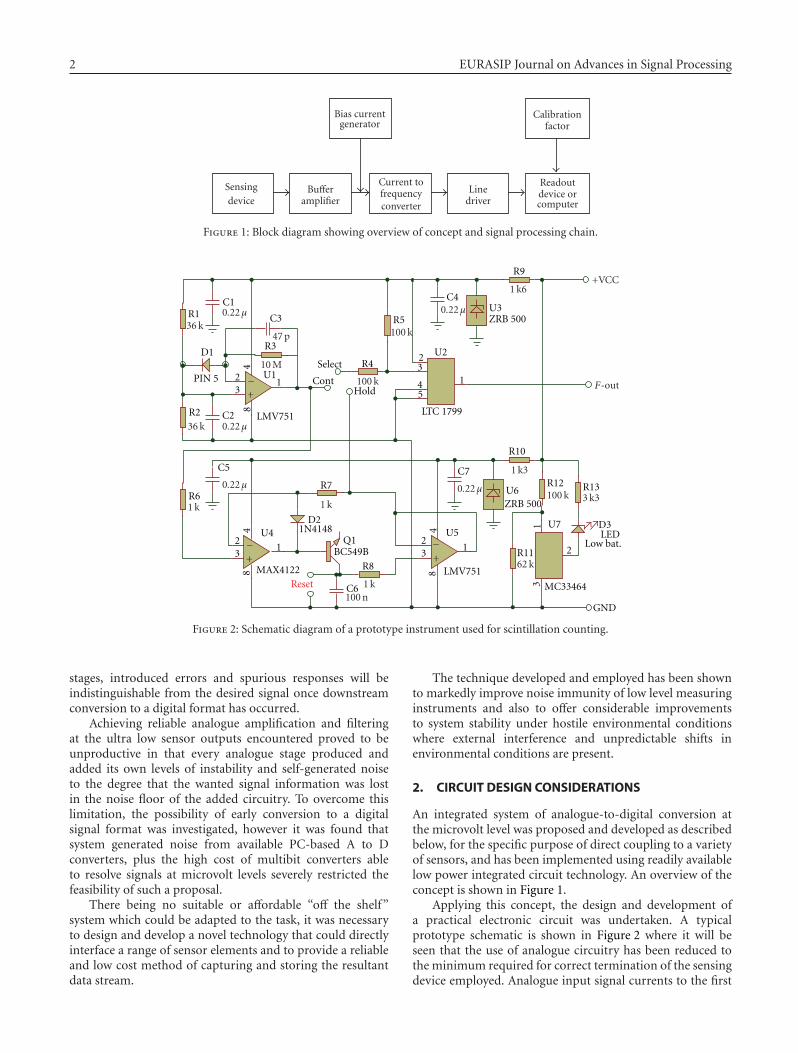
Figure 2: Schematic diagram of a prototype instrument used for scintillation counting.
stages, introduced errors and spurious responses will beindistinguishable from the desired signal once downstreamconversion to a digital format has occurred.
Achieving reliable analogue amplification and filteringat the ultra low sensor outputs encountered proved to beunproductive in that every analogue stage produced andadded its own levels of instability and self-generated noiseto the degree that the wanted signal information was lostin the noise floor of the added circuitry. To overcome thislimitation, the possibility of early conversion to a digitalsignal format was investigated, however it was found thatsystem generated noise from available PC-based A to Dconverters, plus the high cost of multibit converters ableto resolve signals at microvolt levels severely restricted thefeasibility of such a proposal.
There being no suitable or affordable “off the shelf”system which could be adapted to the task, it was necessaryto design and develop a novel technology that could directlyinterface a range of sensor elements and to provide a reliableand low cost method of capturing and storing the resultantdata stream.
The technique developed and employed has been shownto markedly improve noise immunity of low level measuringinstruments and also to offer considerable improvementsto system stability under hostile environmental conditionswhere external interference and unpredictable shifts inenvironmental conditions are present.
2. CIRCUIT DESIGN CONSIDERATIONS
An integrated system of analogue-to-digital conversion atthe microvolt level was proposed and developed as describedbelow, for the specific purpose of direct coupling to a varietyof sensors, and has been implemented using readily availablelow power integrated circuit technology. An overview of theconcept is shown in Figure 1.
Applying this concept, the design and development ofa practical electronic circuit was undertaken. A typicalprototype schematic is shown in Figure 2 where it will beseen that the use of analogue circuitry has been reduced tothe minimum required for correct termination of the sensingdevice employed. Analogue input signal currents to the first
K. Williams and N. Robinson 3
stage device U2 can be less than a microamp and yet producea reliable response.
The particular configuration shown in Figure 2 employsa photodiode sensor in an instrument intended to be used asa scintillation counter. The buffered voltage from the sensoris coupled via a resistance selected to provide the requiredlevel of current injection into pin 3 of U2. A bias currentgenerator adds a fixed current to enable an appropriatebaseline to be set. The functions of U4 and U5 are not part ofthe conversion process but have been added in this instanceto provide a conventional sample and hold facility which, inthe case of a hand-held instrument, allows for a “snapshot”of the data stream to be made manually at a time chosen bythe operator. Use of this additional facility does not interruptthe data stream being processed and stored by an associatedpersonal computer (PC). The base collector junction of Q1 isused for reverse voltage blocking and level shifting and couldbe replaced with a low leakage diode if desired. Device U7is a battery condition indicator and may be omitted if theinstrument is to be mains powered.
Once conversion from current-to-frequency has beenperformed by U1 and U2 the resulting logic level data stream,which has a pulse rate directly proportional to the electricaloutput of the sensor, is passed to a line drive circuit U8(not shown). The low output impedance of this device iscapable of direct connection to a readout device such asfrequency meter or pulse counter, or of driving tens of metresof coaxial cable for remote connection to a PC or data loggerwhere further analysis and storage of measurement data canoccur.
The change in output frequency bears a linear relation-ship to the magnitude of the sensed phenomena, thus it isonly necessary to include an appropriate calibration factorin order to provide automatic interpretation of the outputpulse train and to offer a direct readout in the numericalunits desired. In the case of PC-based data storage, a simplealgorithm and graphing software may be used to provide adirect scaled onscreen display.
Employing modern low power surface mount compo-nents to conserve space and to enhance battery life, aNational Semiconductor LMV 751 [4] low voltage opera-tional amplifier is used as the buffer stage required to inter-face the detector, in this case a precision photodiode, UDTSensors PIN 5DPI, with a current-to-frequency converter.
It is important to keep the gain of this analogue stage toa minimum as it is the primary source of circuit generatednoise. In practice it has been shown that a gain of tencombined with its impedance matching function is adequate,although gains of up to 40 have been used effectively whereminute signal levels need to be accommodated.
Output from this stage is coupled through a 10 kΩ or100 kΩ precision resistor (R4) to set the required conversiongain and thence to the current injection input of currentcontrolled oscillator U2.
The DC supply for the circuit comprises a 9-volt batteryregulated down to 5 volt by the use of a temperaturecompensated, surface mount bandgap reference device. Thissupplies a highly stable +5 volt to the active devices. Thevery low current drain of the circuit allows the use of this
ultrastable and low noise method of regulation, in preferenceto the considerably less precise commonly employed three-terminal voltage regulator integrated circuit.
The output signal characteristics of U2, in this casean LTC 1799 [5], are a considerable improvement overthe older industry standard LM 331N devices and arecompatible with typical logic level specifications. No furtherwaveform processing is required between this point and thefrequency counter unless a remote monitoring facility isrequired. In this case, normal instrumentation practice callsfor a conventional cable driver stage to be added in orderto preserve waveform integrity and device stability whendriving the reactive elements of a long run of coaxial cable.
3. SIGNAL RESOLUTION
To establish resolution, accuracy, and repeatability of mea-surements it was necessary to quantify the level of residualnoise from the analogue stage plus its stability over time, asany drift in the DC bias level arising from the buffer stagewould be additive and indistinguishable from the wantedinput signal. A UDT PIN 5DPI precision photodiode wasused as a sensor during these tests and measurements. Thedata obtained was then used to establish the sensitivityand margins of uncertainty in the current-to-frequencyconversion process.
A precise reference level used to establish the basefrequency of the current-to-frequency converter stage wasgenerated using a high-precision temperature compensatedlaboratory standard which may be regarded as sufficientlystable for the purposes of providing a reference currentsource for the instrument. After an initial warmup periodof 15 minutes to obtain thermal equilibrium of the circuitsinside the sealed instrument case, measurement of voltagefrom the buffer stage to a 10 000Ω input resistor to thecurrent-to-frequency converter was made using a precisiondata acquisition system having a base resolution of 100 μV.
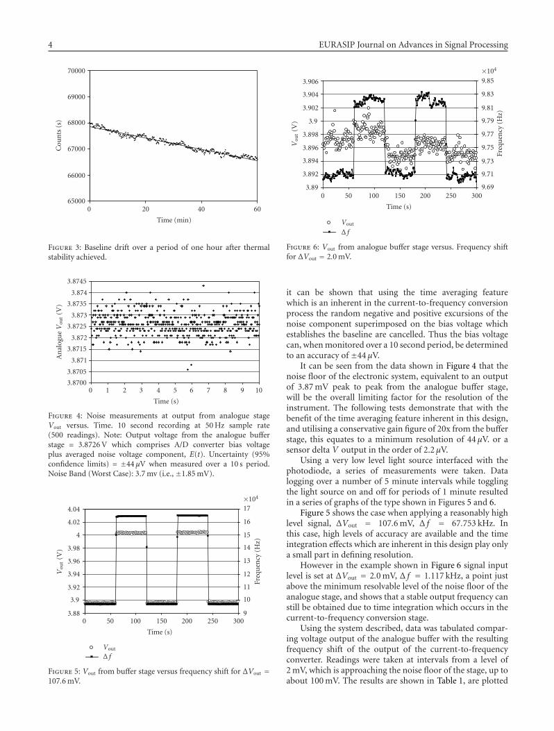
During this test no light was allowed to reach thephotodiode. Bearing in mind the adequate but limiting factorof the 100 μV resolution for the measuring equipment, theinput voltage noise floor and drift of the instrument’s inputstages were logged and the results are shown graphically inFigures 3 and 4 below. These noise voltages are related to theinput current to the current-to-frequency converter stage bythe function E(t) = 10 000I(t).
Figure 3 shows the low level of baseline drift of about19 Hz/min. after initial component thermal stability hasbeen attained. This represents a level of output signal driftin the order of 0.02% per minute. Since most clinicalmeasurements may be taken over durations shorter than aminute, this level of drift would not be significant.
The horizontal bands evident in Figure 4 are an artefactof the lower limit of resolution (100 μV) achievable from thedata acquisition system used in capturing this informationand are not in any way a function of the buffer or frequencyconversion. It can be seen that the characteristic of thetotal circuit and incidental noise is random with a worst-case peak to peak spread of 3.87 mV. As the negative andpositive excursions are relatively uniform about a mean,
4 EURASIP Journal on Advances in Signal Processing
0 20 40 60
Time (min)
65000
66000
67000
68000
69000
70000
Cou
nts
(s)
Figure 3: Baseline drift over a period of one hour after thermalstability achieved.
0 1 2 3 4 5 6 7 8 9 10
Time (s)
3.8700
3.8705
3.871
3.8715
3.872
3.8725
3.873
3.8735
3.874
3.8745
An
alog
ueV
out
(V)
Figure 4: Noise measurements at output from analogue stageVout versus. Time. 10 second recording at 50 Hz sample rate(500 readings). Note: Output voltage from the analogue bufferstage = 3.8726 V which comprises A/D converter bias voltageplus averaged noise voltage component, E(t). Uncertainty (95%confidence limits) = ±44 μV when measured over a 10 s period.Noise Band (Worst Case): 3.7 mv (i.e., ±1.85 mV).
0 50 100 150 200 250 300
Time (s)
3.88
3.9
3.92
3.94
3.96
3.98
4
4.02
4.04
Vou
t(V
)
9
10
11
12
13
14
15
16
17×104
Freq
uen
cy(H
z)
Vout
Δ f
Figure 5: Vout from buffer stage versus frequency shift for ΔVout =107.6 mV.
0 50 100 150 200 250 300
Time (s)
3.89
3.892
3.894
3.896
3.898
3.9
3.902
3.904
3.906
Vou
t(V
)
9.69
9.71
9.73
9.75
9.77
9.79
9.81
9.83
9.85×10⁴
Freq
uen
cy(H
z)
Vout
Δ f
Figure 6: Vout from analogue buffer stage versus. Frequency shiftfor ΔVout = 2.0 mV.
it can be shown that using the time averaging featurewhich is an inherent in the current-to-frequency conversionprocess the random negative and positive excursions of thenoise component superimposed on the bias voltage whichestablishes the baseline are cancelled. Thus the bias voltagecan, when monitored over a 10 second period, be determinedto an accuracy of ±44 μV.
It can be seen from the data shown in Figure 4 that thenoise floor of the electronic system, equivalent to an outputof 3.87 mV peak to peak from the analogue buffer stage,will be the overall limiting factor for the resolution of theinstrument. The following tests demonstrate that with thebenefit of the time averaging feature inherent in this design,and utilising a conservative gain figure of 20x from the bufferstage, this equates to a minimum resolution of 44 μV. or asensor delta V output in the order of 2.2 μV.
Using a very low level light source interfaced with thephotodiode, a series of measurements were taken. Datalogging over a number of 5 minute intervals while togglingthe light source on and off for periods of 1 minute resultedin a series of graphs of the type shown in Figures 5 and 6.
Figure 5 shows the case when applying a reasonably highlevel signal, ΔVout = 107.6 mV, Δ f = 67.753 kHz. Inthis case, high levels of accuracy are available and the timeintegration effects which are inherent in this design play onlya small part in defining resolution.
However in the example shown in Figure 6 signal inputlevel is set at ΔVout = 2.0 mV, Δ f = 1.117 kHz, a point justabove the minimum resolvable level of the noise floor of theanalogue stage, and shows that a stable output frequency canstill be obtained due to time integration which occurs in thecurrent-to-frequency conversion stage.
Using the system described, data was tabulated compar-ing voltage output of the analogue buffer with the resultingfrequency shift of the output of the current-to-frequencyconverter. Readings were taken at intervals from a level of2 mV, which is approaching the noise floor of the stage, up toabout 100 mV. The results are shown in Table 1, are plotted
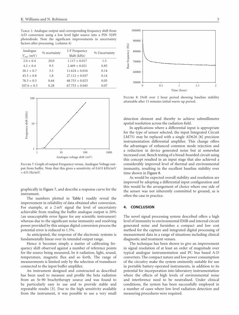
K. Williams and N. Robinson 5
Table 1: Analogue output and corresponding frequency shift fromA/D conversion using a low level light source into a PIN 5DPIphotodiode. Note the significant improvements in uncertaintyfactors after processing. (column 4)
Analogue% ncertainty
I-F Frequency% Uncertainty
Vout (mV) Shift (kHz)
2.0± 0.4 20.0 1.117± 0.017 1.5
4.2± 0.4 9.5 2.469± 0.021 0.85
20.1± 0.7 3.5 11.624± 0.016 0.14
45.5± 0.8 1.8 27.112± 0.037 0.14
78.3± 0.5 0.64 48.753± 0.023 0.05
107.6± 0.3 0.28 67.753± 0.045 0.07
1 10 100 1000
Analogue voltage shift (mV)
1
10
100
Freq
uen
cysh
ift
(kH
z)
Figure 7: Graph of output Frequency versus. Analogue Voltage out-put from buffer. Note that this gives a sensitivity of 0.631 kHz/mV= 631 Hz/mV.
graphically in Figure 7, and describe a response curve for theinstrument.
The numbers plotted in Table 1 readily reveal theimprovement in reliability of data obtained after conversion.For example, at a 2 mV signal the level of uncertaintyachievable from reading the buffer analogue output is 20%(an unacceptable error figure for any scientific instrument)whereas due to the significant noise immunity and resolvingpower provided by this unique digital conversion process thepotential error is reduced to 1.5%.
As anticipated, the response of the electronic systems isfundamentally linear over its intended output range.
Hence it becomes simply a matter of calibrating fre-quency shift observed against a number of reference pointsfor the source being measured, be it radiation, light, sound,temperature, magnetic flux and so forth. The range ofmeasurements is limited only by the selection of transducerconnected to the input buffer amplifier.
An instrument designed and constructed as describedhas been used to measure and profile the beta radiationfrom an Sr-90 brachytherapy source and was found tobe particularly easy to use and to provide stable andrepeatable results [3]. Due to the high sensitivity availablefrom the instrument, it was possible to use a very small
0 0.5 1 1.5 2
Time (hour)
50000
60000
70000
80000
90000
100000
Bas
efr
equ
ency
(Hz)
Figure 8: Drift over 2 hour period showing baseline stabilityattainable after 15 minutes initial warm-up period.
detection element and thereby to achieve submillimetrespatial resolution across the radiation field.
In applications where a differential input is appropriatefor the type of sensor selected, the input Integrated CircuitLM751 may be replaced with a single AD626 [6] precisioninstrumentation differential amplifier. This change offersthe advantages of enhanced common mode rejection anda reduction in device generated noise but at somewhatincreased cost. Bench testing of a bread-boarded circuit usingthis concept resulted in an input stage that also achieved aconsiderably improved level of thermal and environmentalimmunity, resulting in the excellent baseline stability overtime shown in Figure 8.
As would be expected overall stability and resolution areimproved by adopting a differential input configuration andthis would be the arrangement of choice where one side ofthe sensor was not inherently committed to ground, as isoften the case in practice.
4. CONCLUSION
The novel signal processing system described offers a highlevel of immunity to environmental EMR and internal circuitgenerated noise and furnishes a compact and low costmethod for the capture and integrated digital processing ofmeasurement data in a range of situations including clinicaldiagnostic and treatment venues.
The technique has been shown to give an improvementin signal resolution of at least an order of magnitude overtypical analogue instrumentation and PC bus based A-Dconverters. The compact nature and low power consumptionof the circuitry make the system eminently suitable for usein portable battery-operated instruments, in addition to itspotential for incorporation into laboratory instrumentationwhere the effects of high levels of environmental noiseand interference need to be neutralised. Under clinicalconditions, the system has been successfully employed ina number of cases where low level radiation detection andmeasuring procedures were required.
6 EURASIP Journal on Advances in Signal Processing
Coupled with an organic plastic scintillation elementfor detection and measurement of X rays, a prototypeinstrument incorporating this method of signal capture andprocessing has been found to be particularly effective inproviding direct readout of high intensity photon beams gen-erated by clinical linear accelerators in situations involvinghigh levels of background radiation and interference andwhere remote monitoring at distances of up to 30 metresfrom the detector has been required.
REFERENCES
[1] M. A. Clift, R. A. Sutton, and D. V. Webb, “Water equivalenceof plastic organic scintillators in megavoltage radiotherapybremsstrahlung beams,” Physics in Medicine and Biology, vol.45, no. 7, pp. 1885–1895, 2000.
[2] K. Williams, N. Robinson, J. Trapp, et al., “A portable organicplastic scintillator dosimetry system for low energy X-rays:a feasibility study using an intraoperative X-ray unit as theradiation source,” Journal of Medical Physics, vol. 32, no. 2, pp.73–76, 2007.
[3] M. Geso, N. Robinson, W. Schumer, and K. Williams,“Use of water-equivalent plastic scintillator for intravascularbrachytherapy dosimetry,” Australasian Physical & EngineeringSciences in Medicine, vol. 27, no. 1, pp. 5–10, 2004.
[4] http://www.national.com/catalog/.[5] http://www.linearteck.com/.[6] http://www.analog.com/product.


![SingaporeManagementUniversity arXiv:1801.00973v1 [econ.EM ... · arXiv:1801.00973v1 [econ.EM] 3 Jan 2018 A New Wald Test for Hypothesis Testing Based on MCMC outputs∗ YongLi RenminUniversity](https://static.fdocument.org/doc/165x107/5e8fba5a2e14ec660816560a/singaporemanagementuniversity-arxiv180100973v1-econem-arxiv180100973v1.jpg)