24C02C - Microchip Technologyww1.microchip.com/downloads/en/DeviceDoc/21202J.pdf · 24C02C...
30
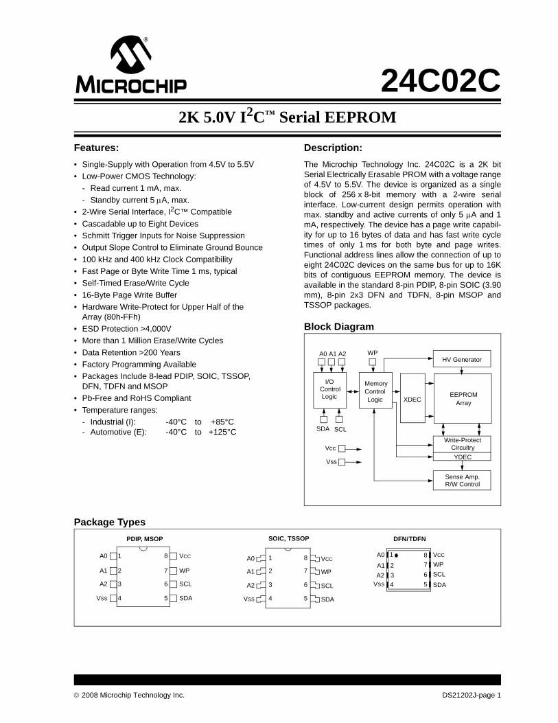
© 2008 Microchip Technology Inc. DS21202J-page 1 24C02C Features: • Single-Supply with Operation from 4.5V to 5.5V • Low-Power CMOS Technology: - Read current 1 mA, max. - Standby current 5 μA, max. • 2-Wire Serial Interface, I 2 C™ Compatible • Cascadable up to Eight Devices • Schmitt Trigger Inputs for Noise Suppression • Output Slope Control to Eliminate Ground Bounce • 100 kHz and 400 kHz Clock Compatibility • Fast Page or Byte Write Time 1 ms, typical • Self-Timed Erase/Write Cycle • 16-Byte Page Write Buffer • Hardware Write-Protect for Upper Half of the Array (80h-FFh) • ESD Protection >4,000V • More than 1 Million Erase/Write Cycles • Data Retention >200 Years • Factory Programming Available • Packages Include 8-lead PDIP, SOIC, TSSOP, DFN, TDFN and MSOP • Pb-Free and RoHS Compliant • Temperature ranges: Description: The Microchip Technology Inc. 24C02C is a 2K bit Serial Electrically Erasable PROM with a voltage range of 4.5V to 5.5V. The device is organized as a single block of 256 x 8-bit memory with a 2-wire serial interface. Low-current design permits operation with max. standby and active currents of only 5 μA and 1 mA, respectively. The device has a page write capabil- ity for up to 16 bytes of data and has fast write cycle times of only 1 ms for both byte and page writes. Functional address lines allow the connection of up to eight 24C02C devices on the same bus for up to 16K bits of contiguous EEPROM memory. The device is available in the standard 8-pin PDIP, 8-pin SOIC (3.90 mm), 8-pin 2x3 DFN and TDFN, 8-pin MSOP and TSSOP packages. Block Diagram Package Types - Industrial (I): -40°C to +85°C - Automotive (E): -40°C to +125°C I/O Control Logic Memory Control Logic XDEC HV Generator EEPROM Array Write-Protect Circuitry YDEC Vcc Vss Sense Amp. R/W Control SDA SCL A0 A1 A2 WP A0 A1 A2 VSS VCC WP SCL SDA 1 2 3 4 8 7 6 5 PDIP, MSOP SOIC, TSSOP A0 A1 A2 VSS 1 2 3 4 8 7 6 5 VCC WP SCL SDA DFN/TDFN A0 A1 A2 VSS WP SCL SDA VCC 8 7 6 5 1 2 3 4 2K 5.0V I 2 C ™ Serial EEPROM
Transcript of 24C02C - Microchip Technologyww1.microchip.com/downloads/en/DeviceDoc/21202J.pdf · 24C02C...
24C02C2K 5.0V I2C™ Serial EEPROM
Features:• Single-Supply with Operation from 4.5V to 5.5V• Low-Power CMOS Technology:
- Read current 1 mA, max.- Standby current 5 μA, max.
• 2-Wire Serial Interface, I2C™ Compatible• Cascadable up to Eight Devices• Schmitt Trigger Inputs for Noise Suppression• Output Slope Control to Eliminate Ground Bounce• 100 kHz and 400 kHz Clock Compatibility• Fast Page or Byte Write Time 1 ms, typical• Self-Timed Erase/Write Cycle• 16-Byte Page Write Buffer• Hardware Write-Protect for Upper Half of the
Array (80h-FFh)• ESD Protection >4,000V• More than 1 Million Erase/Write Cycles• Data Retention >200 Years• Factory Programming Available• Packages Include 8-lead PDIP, SOIC, TSSOP,
DFN, TDFN and MSOP• Pb-Free and RoHS Compliant• Temperature ranges:
Description:The Microchip Technology Inc. 24C02C is a 2K bitSerial Electrically Erasable PROM with a voltage rangeof 4.5V to 5.5V. The device is organized as a singleblock of 256 x 8-bit memory with a 2-wire serialinterface. Low-current design permits operation withmax. standby and active currents of only 5 μA and 1mA, respectively. The device has a page write capabil-ity for up to 16 bytes of data and has fast write cycletimes of only 1 ms for both byte and page writes.Functional address lines allow the connection of up toeight 24C02C devices on the same bus for up to 16Kbits of contiguous EEPROM memory. The device isavailable in the standard 8-pin PDIP, 8-pin SOIC (3.90mm), 8-pin 2x3 DFN and TDFN, 8-pin MSOP andTSSOP packages.
Block Diagram
Package Types
- Industrial (I): -40°C to +85°C- Automotive (E): -40°C to +125°C
I/OControl Logic
MemoryControl Logic XDEC
HV Generator
EEPROM Array
Write-Protect Circuitry
YDECVcc
Vss
Sense Amp.R/W Control
SDA SCL
A0 A1 A2 WP
A0
A1
A2
VSS
VCC
WP
SCL
SDA
1
2
3
4
8
7
6
5
PDIP, MSOP SOIC, TSSOP
A0
A1
A2
VSS
1
2
3
4
8
7
6
5
VCC
WP
SCL
SDA
DFN/TDFN
A0
A1A2
VSS
WPSCL
SDA
VCC8765
1
234
© 2008 Microchip Technology Inc. DS21202J-page 1
24C02C
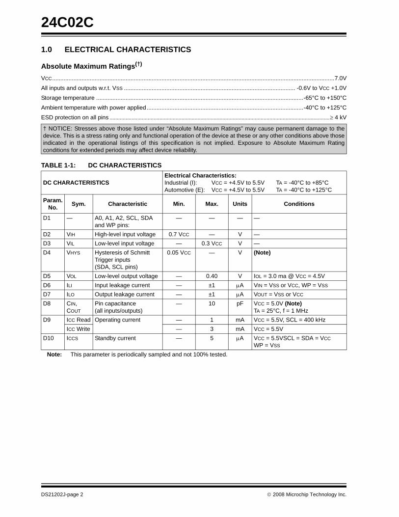
1.0 ELECTRICAL CHARACTERISTICS
Absolute Maximum Ratings(†)
VCC.............................................................................................................................................................................7.0V
All inputs and outputs w.r.t. VSS ......................................................................................................... -0.6V to VCC +1.0V
Storage temperature ...............................................................................................................................-65°C to +150°C
Ambient temperature with power applied................................................................................................-40°C to +125°C
ESD protection on all pins ......................................................................................................................................................≥ 4 kV
TABLE 1-1: DC CHARACTERISTICS
† NOTICE: Stresses above those listed under “Absolute Maximum Ratings” may cause permanent damage to thedevice. This is a stress rating only and functional operation of the device at these or any other conditions above thoseindicated in the operational listings of this specification is not implied. Exposure to Absolute Maximum Ratingconditions for extended periods may affect device reliability.
DC CHARACTERISTICSElectrical Characteristics:Industrial (I): VCC = +4.5V to 5.5V TA = -40°C to +85°CAutomotive (E): VCC = +4.5V to 5.5V TA = -40°C to +125°C
Param.No. Sym. Characteristic Min. Max. Units Conditions
D1 — A0, A1, A2, SCL, SDA and WP pins:
— — — —
D2 VIH High-level input voltage 0.7 VCC — V —D3 VIL Low-level input voltage — 0.3 VCC V —D4 VHYS Hysteresis of Schmitt
Trigger inputs(SDA, SCL pins)
0.05 VCC — V (Note)
D5 VOL Low-level output voltage — 0.40 V IOL = 3.0 ma @ VCC = 4.5VD6 ILI Input leakage current — ±1 μA VIN = VSS or VCC, WP = VSS
D7 ILO Output leakage current — ±1 μA VOUT = VSS or VCC
D8 CIN, COUT
Pin capacitance (all inputs/outputs)
— 10 pF VCC = 5.0V (Note)TA = 25°C, f = 1 MHz
D9 ICC Read Operating current — 1 mA VCC = 5.5V, SCL = 400 kHzICC Write — 3 mA VCC = 5.5V
D10 ICCS Standby current — 5 μA VCC = 5.5VSCL = SDA = VCCWP = VSS
Note: This parameter is periodically sampled and not 100% tested.
DS21202J-page 2 © 2008 Microchip Technology Inc.
24C02C
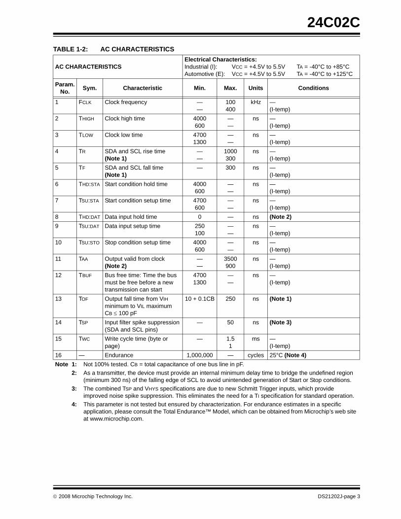
TABLE 1-2: AC CHARACTERISTICSAC CHARACTERISTICSElectrical Characteristics:Industrial (I): VCC = +4.5V to 5.5V TA = -40°C to +85°CAutomotive (E): VCC = +4.5V to 5.5V TA = -40°C to +125°C
Param.No. Sym. Characteristic Min. Max. Units Conditions
1 FCLK Clock frequency ——
100400
kHz —(I-temp)
2 THIGH Clock high time 4000600
——
ns —(I-temp)
3 TLOW Clock low time 47001300
——
ns —(I-temp)
4 TR SDA and SCL rise time (Note 1)
——
1000300
ns —(I-temp)
5 TF SDA and SCL fall time (Note 1)
— 300 ns —(I-temp)
6 THD:STA Start condition hold time 4000600
——
ns —(I-temp)
7 TSU:STA Start condition setup time 4700600
——
ns —(I-temp)
8 THD:DAT Data input hold time 0 — ns (Note 2)9 TSU:DAT Data input setup time 250
100——
ns —(I-temp)
10 TSU:STO Stop condition setup time 4000600
——
ns —(I-temp)
11 TAA Output valid from clock (Note 2)
——
3500900
ns —(I-temp)
12 TBUF Bus free time: Time the bus must be free before a new transmission can start
47001300
——
ns —(I-temp)
13 TOF Output fall time from VIHminimum to VIL maximumCB ≤ 100 pF
10 + 0.1CB 250 ns (Note 1)
14 TSP Input filter spike suppression(SDA and SCL pins)
— 50 ns (Note 3)
15 TWC Write cycle time (byte or page)
— 1.51
ms —(I-temp)
16 — Endurance 1,000,000 — cycles 25°C (Note 4)Note 1: Not 100% tested. CB = total capacitance of one bus line in pF.
2: As a transmitter, the device must provide an internal minimum delay time to bridge the undefined region (minimum 300 ns) of the falling edge of SCL to avoid unintended generation of Start or Stop conditions.
3: The combined TSP and VHYS specifications are due to new Schmitt Trigger inputs, which provide improved noise spike suppression. This eliminates the need for a TI specification for standard operation.
4: This parameter is not tested but ensured by characterization. For endurance estimates in a specific application, please consult the Total Endurance™ Model, which can be obtained from Microchip’s web site at www.microchip.com.
© 2008 Microchip Technology Inc. DS21202J-page 3
24C02C
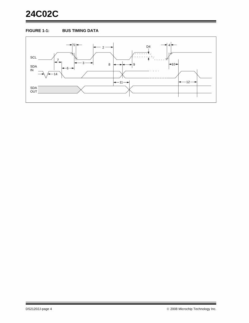
FIGURE 1-1: BUS TIMING DATASCL
SDAIN
SDAOUT
5
7
6
14
3
2
8 9
11
D4 4
10
12
DS21202J-page 4 © 2008 Microchip Technology Inc.
24C02C
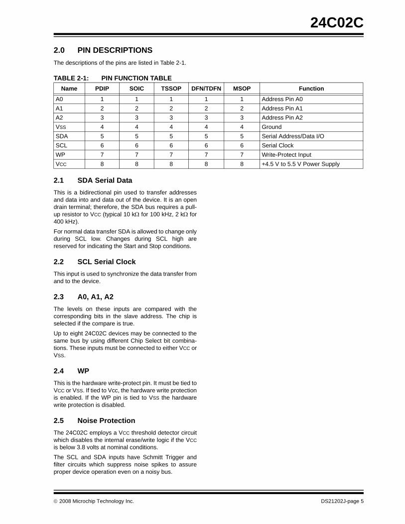
2.0 PIN DESCRIPTIONSThe descriptions of the pins are listed in Table 2-1.
TABLE 2-1: PIN FUNCTION TABLE
2.1 SDA Serial DataThis is a bidirectional pin used to transfer addressesand data into and data out of the device. It is an opendrain terminal; therefore, the SDA bus requires a pull-up resistor to VCC (typical 10 kΩ for 100 kHz, 2 kΩ for400 kHz).
For normal data transfer SDA is allowed to change onlyduring SCL low. Changes during SCL high arereserved for indicating the Start and Stop conditions.
2.2 SCL Serial Clock This input is used to synchronize the data transfer fromand to the device.
2.3 A0, A1, A2The levels on these inputs are compared with thecorresponding bits in the slave address. The chip isselected if the compare is true.
Up to eight 24C02C devices may be connected to thesame bus by using different Chip Select bit combina-tions. These inputs must be connected to either VCC orVSS.
2.4 WPThis is the hardware write-protect pin. It must be tied toVCC or VSS. If tied to Vcc, the hardware write protectionis enabled. If the WP pin is tied to VSS the hardwarewrite protection is disabled.
2.5 Noise ProtectionThe 24C02C employs a VCC threshold detector circuitwhich disables the internal erase/write logic if the VCCis below 3.8 volts at nominal conditions.
The SCL and SDA inputs have Schmitt Trigger andfilter circuits which suppress noise spikes to assureproper device operation even on a noisy bus.
Name PDIP SOIC TSSOP DFN/TDFN MSOP Function
A0 1 1 1 1 1 Address Pin A0A1 2 2 2 2 2 Address Pin A1A2 3 3 3 3 3 Address Pin A2VSS 4 4 4 4 4 GroundSDA 5 5 5 5 5 Serial Address/Data I/OSCL 6 6 6 6 6 Serial ClockWP 7 7 7 7 7 Write-Protect InputVCC 8 8 8 8 8 +4.5 V to 5.5 V Power Supply
© 2008 Microchip Technology Inc. DS21202J-page 5
24C02C
3.0 FUNCTIONAL DESCRIPTIONSThe 24C02C supports a bidirectional 2-wire bus anddata transmission protocol. A device that sends dataonto the bus is defined as transmitter, and a devicereceiving data as receiver. The bus has to be controlledby a master device that generates the Serial Clock(SCL), controls the bus access, and generates the Startand Stop conditions, while the 24C02C works as slave.Both master and slave can operate as transmitter orreceiver but the master device determines which modeis activated.
4.0 BUS CHARACTERISTICSThe following bus protocol has been defined:
• Data transfer may be initiated only when the bus is not busy.
• During data transfer, the data line must remain stable whenever the clock line is high. Changes in the data line while the clock line is high will be interpreted as a Start or Stop condition.
Accordingly, the following bus conditions have beendefined (Figure 4-1).
4.1 Bus Not Busy (A)Both data and clock lines remain high.
4.2 Start Data Transfer (B)A high-to-low transition of the SDA line while the clock(SCL) is high determines a Start condition. Allcommands must be preceded by a Start condition.
4.3 Stop Data Transfer (C)A low-to-high transition of the SDA line while the clock(SCL) is high determines a Stop condition. All opera-tions must be ended with a Stop condition.
4.4 Data Valid (D)The state of the data line represents valid data when,after a Start condition, the data line is stable for theduration of the high period of the clock signal.
The data on the line must be changed during the lowperiod of the clock signal. There is one bit of data perclock pulse.
Each data transfer is initiated with a Start condition andterminated with a Stop condition. The number of thedata bytes transferred between the Start and Stopconditions is determined by the master device and istheoretically unlimited, although only the last sixteenwill be stored when doing a write operation. When anoverwrite does occur it will replace data in a first-in first-out fashion.
4.5 AcknowledgeEach receiving device, when addressed, is required togenerate an acknowledge after the reception of eachbyte. The master device must generate an extra clockpulse, which is associated with this Acknowledge bit.
The device that acknowledges has to pull down theSDA line during the Acknowledge clock pulse in such away that the SDA line is stable low during the highperiod of the acknowledge related clock pulse. Ofcourse, setup and hold times must be taken intoaccount. A master must signal an end of data to theslave by not generating an Acknowledge bit on the lastbyte that has been clocked out of the slave. In thiscase, the slave must leave the data line high to enablethe master to generate the Stop condition (Figure 4-2).
Note: The 24C02C does not generate any Acknowledge bits if an internal programming cycle is in progress.
DS21202J-page 6 © 2008 Microchip Technology Inc.
24C02C
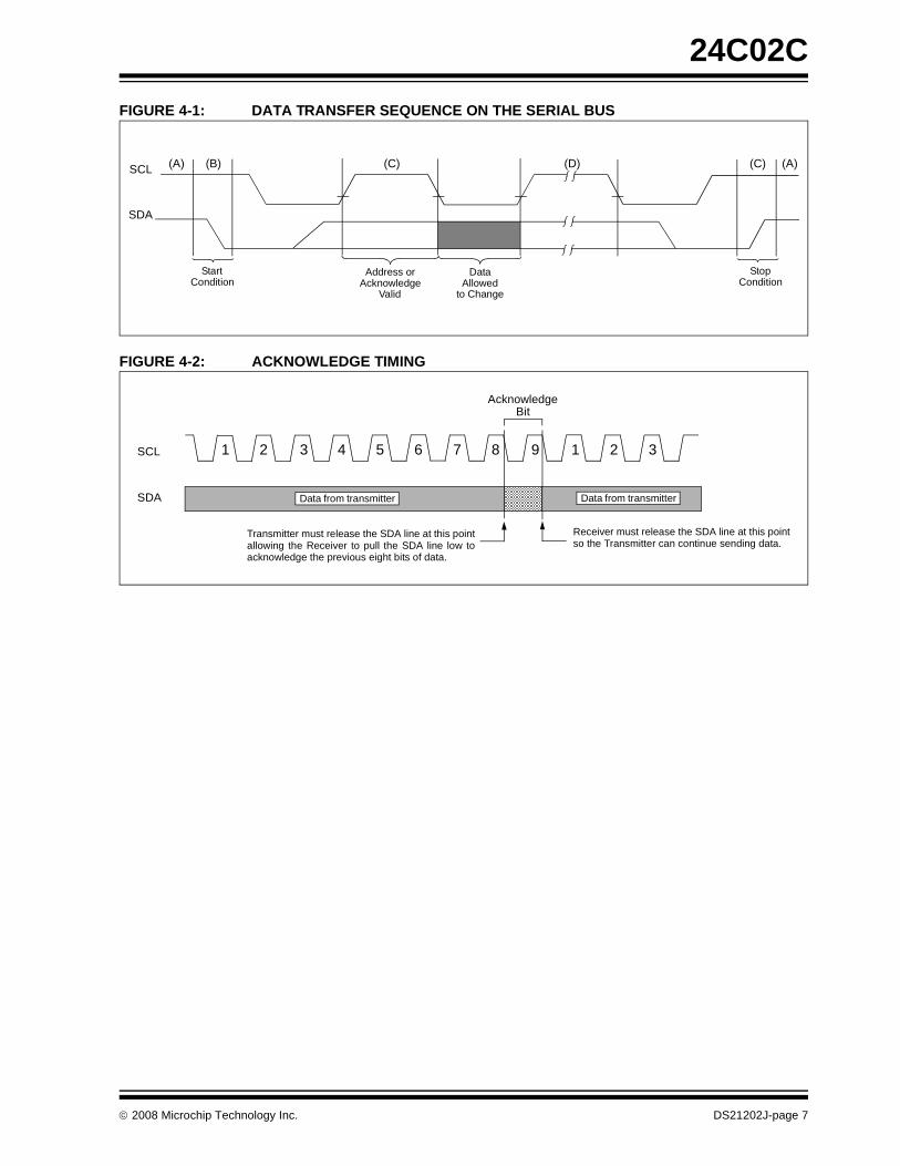
FIGURE 4-1: DATA TRANSFER SEQUENCE ON THE SERIAL BUSFIGURE 4-2: ACKNOWLEDGE TIMING
(A) (B) (C) (D) (A)(C)SCL
SDA
StartCondition
Address orAcknowledge
Valid
DataAllowed
to Change
StopCondition
SCL 987654321 1 2 3
Transmitter must release the SDA line at this pointallowing the Receiver to pull the SDA line low toacknowledge the previous eight bits of data.
Receiver must release the SDA line at this pointso the Transmitter can continue sending data.
Data from transmitter Data from transmitterSDA
AcknowledgeBit
© 2008 Microchip Technology Inc. DS21202J-page 7
24C02C
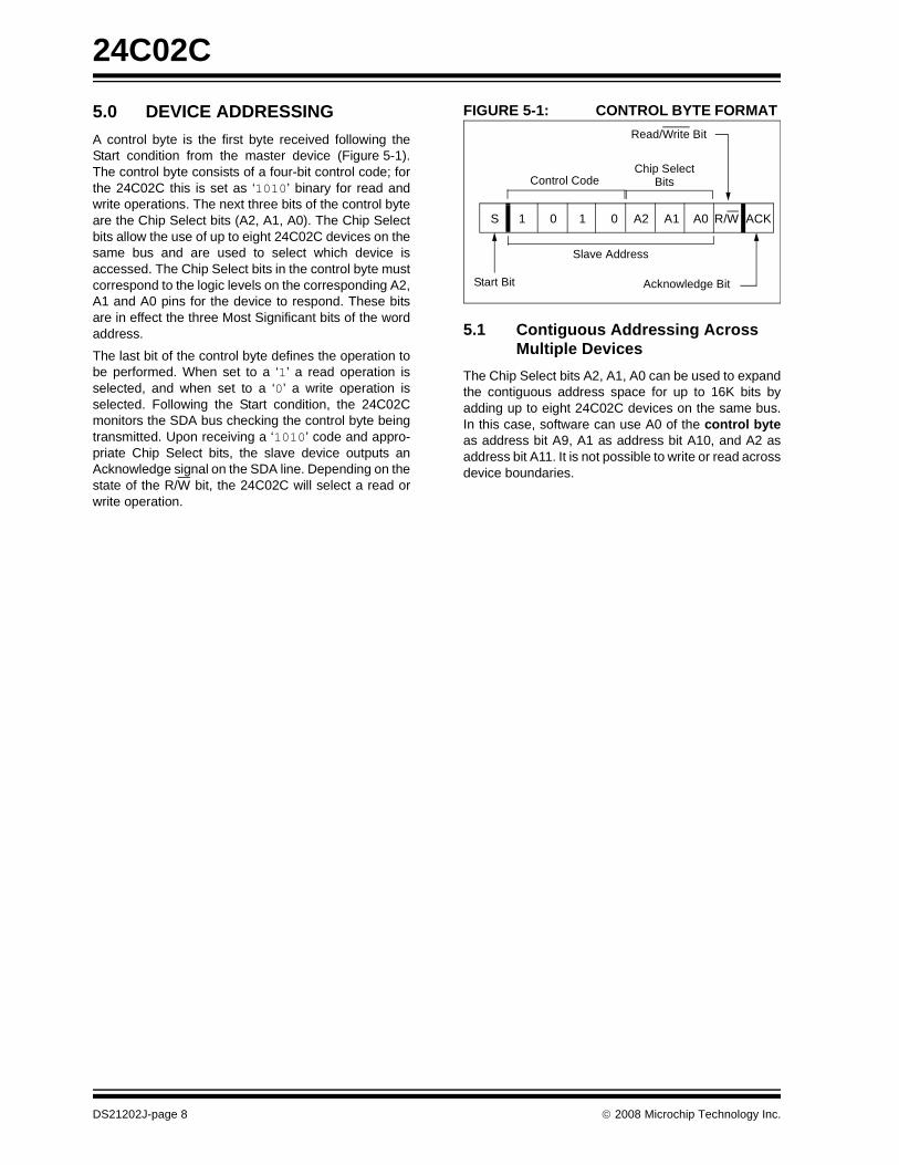
5.0 DEVICE ADDRESSINGA control byte is the first byte received following theStart condition from the master device (Figure 5-1).The control byte consists of a four-bit control code; forthe 24C02C this is set as ‘1010’ binary for read andwrite operations. The next three bits of the control byteare the Chip Select bits (A2, A1, A0). The Chip Selectbits allow the use of up to eight 24C02C devices on thesame bus and are used to select which device isaccessed. The Chip Select bits in the control byte mustcorrespond to the logic levels on the corresponding A2,A1 and A0 pins for the device to respond. These bitsare in effect the three Most Significant bits of the wordaddress.
The last bit of the control byte defines the operation tobe performed. When set to a ‘1’ a read operation isselected, and when set to a ‘0’ a write operation isselected. Following the Start condition, the 24C02Cmonitors the SDA bus checking the control byte beingtransmitted. Upon receiving a ‘1010’ code and appro-priate Chip Select bits, the slave device outputs anAcknowledge signal on the SDA line. Depending on thestate of the R/W bit, the 24C02C will select a read orwrite operation.
FIGURE 5-1: CONTROL BYTE FORMAT
5.1 Contiguous Addressing Across Multiple Devices
The Chip Select bits A2, A1, A0 can be used to expandthe contiguous address space for up to 16K bits byadding up to eight 24C02C devices on the same bus.In this case, software can use A0 of the control byteas address bit A9, A1 as address bit A10, and A2 asaddress bit A11. It is not possible to write or read acrossdevice boundaries.
1 0 1 0 A2 A1 A0S ACKR/W
Control CodeChip Select
Bits
Slave Address
Acknowledge BitStart Bit
Read/Write Bit
DS21202J-page 8 © 2008 Microchip Technology Inc.
24C02C
6.0 WRITE OPERATIONS
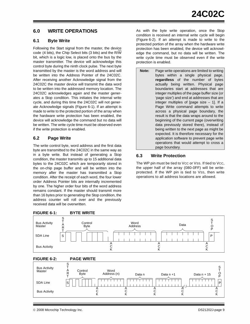
6.1 Byte WriteFollowing the Start signal from the master, the devicecode (4 bits), the Chip Select bits (3 bits) and the R/Wbit, which is a logic low, is placed onto the bus by themaster transmitter. The device will acknowledge thiscontrol byte during the ninth clock pulse. The next bytetransmitted by the master is the word address and willbe written into the Address Pointer of the 24C02C.After receiving another Acknowledge signal from the24C02C the master device will transmit the data wordto be written into the addressed memory location. The24C02C acknowledges again and the master gener-ates a Stop condition. This initiates the internal writecycle, and during this time the 24C02C will not gener-ate Acknowledge signals (Figure 6-1). If an attempt ismade to write to the protected portion of the array whenthe hardware write protection has been enabled, thedevice will acknowledge the command but no data willbe written. The write cycle time must be observed evenif the write protection is enabled.
6.2 Page WriteThe write control byte, word address and the first databyte are transmitted to the 24C02C in the same way asin a byte write. But instead of generating a Stopcondition, the master transmits up to 15 additional databytes to the 24C02C which are temporarily stored inthe on-chip page buffer and will be written into thememory after the master has transmitted a Stopcondition. After the receipt of each word, the four lowerorder Address Pointer bits are internally incrementedby one. The higher order four bits of the word addressremains constant. If the master should transmit morethan 16 bytes prior to generating the Stop condition, theaddress counter will roll over and the previouslyreceived data will be overwritten.
As with the byte write operation, once the Stopcondition is received an internal write cycle will begin(Figure 6-2). If an attempt is made to write to theprotected portion of the array when the hardware writeprotection has been enabled, the device will acknowl-edge the command, but no data will be written. Thewrite cycle time must be observed even if the writeprotection is enabled.
6.3 Write ProtectionThe WP pin must be tied to VCC or VSS. If tied to VCC,the upper half of the array (080-0FF) will be write-protected. If the WP pin is tied to VSS, then writeoperations to all address locations are allowed.
FIGURE 6-1: BYTE WRITE
FIGURE 6-2: PAGE WRITE
Note: Page write operations are limited to writingbytes within a single physical page,regardless of the number of bytesactually being written. Physical pageboundaries start at addresses that areinteger multiples of the page buffer size (or‘page size’) and end at addresses that areinteger multiples of [page size – 1]. If aPage Write command attempts to writeacross a physical page boundary, theresult is that the data wraps around to thebeginning of the current page (overwritingdata previously stored there), instead ofbeing written to the next page as might beexpected. It is therefore necessary for theapplication software to prevent page writeoperations that would attempt to cross apage boundary.
S P
Bus ActivityMaster
SDA Line
Bus Activity
START
STOP
ControlByte
WordAddress Data
ACK
ACK
ACK
S P
Bus ActivityMaster
SDA Line
Bus Activity
START
ControlByte
WordAddress (n) Data n Data n + 15
STOP
ACK
ACK
ACK
ACK
ACK
Data n +1
© 2008 Microchip Technology Inc. DS21202J-page 9
24C02C
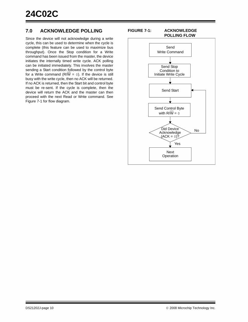
7.0 ACKNOWLEDGE POLLINGSince the device will not acknowledge during a writecycle, this can be used to determine when the cycle iscomplete (this feature can be used to maximize busthroughput). Once the Stop condition for a Writecommand has been issued from the master, the deviceinitiates the internally timed write cycle. ACK pollingcan be initiated immediately. This involves the mastersending a Start condition followed by the control bytefor a Write command (R/W = 0). If the device is stillbusy with the write cycle, then no ACK will be returned.If no ACK is returned, then the Start bit and control bytemust be re-sent. If the cycle is complete, then thedevice will return the ACK and the master can thenproceed with the next Read or Write command. SeeFigure 7-1 for flow diagram.
FIGURE 7-1: ACKNOWLEDGE POLLING FLOW
SendWrite Command
Send StopCondition to
Initiate Write Cycle
Send Start
Send Control Bytewith R/W = 0
Did DeviceAcknowledge(ACK = 0)?
NextOperation
No
Yes
DS21202J-page 10 © 2008 Microchip Technology Inc.
24C02C
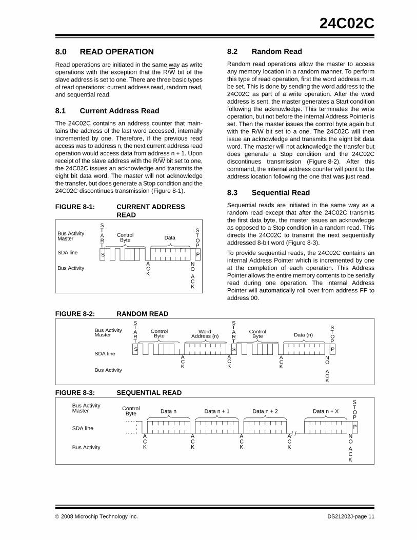
8.0 READ OPERATIONRead operations are initiated in the same way as writeoperations with the exception that the R/W bit of theslave address is set to one. There are three basic typesof read operations: current address read, random read,and sequential read.
8.1 Current Address ReadThe 24C02C contains an address counter that main-tains the address of the last word accessed, internallyincremented by one. Therefore, if the previous readaccess was to address n, the next current address readoperation would access data from address n + 1. Uponreceipt of the slave address with the R/W bit set to one,the 24C02C issues an acknowledge and transmits theeight bit data word. The master will not acknowledgethe transfer, but does generate a Stop condition and the24C02C discontinues transmission (Figure 8-1).
FIGURE 8-1: CURRENT ADDRESS READ
8.2 Random ReadRandom read operations allow the master to accessany memory location in a random manner. To performthis type of read operation, first the word address mustbe set. This is done by sending the word address to the24C02C as part of a write operation. After the wordaddress is sent, the master generates a Start conditionfollowing the acknowledge. This terminates the writeoperation, but not before the internal Address Pointer isset. Then the master issues the control byte again butwith the R/W bit set to a one. The 24C02C will thenissue an acknowledge and transmits the eight bit dataword. The master will not acknowledge the transfer butdoes generate a Stop condition and the 24C02Cdiscontinues transmission (Figure 8-2). After thiscommand, the internal address counter will point to theaddress location following the one that was just read.
8.3 Sequential ReadSequential reads are initiated in the same way as arandom read except that after the 24C02C transmitsthe first data byte, the master issues an acknowledgeas opposed to a Stop condition in a random read. Thisdirects the 24C02C to transmit the next sequentiallyaddressed 8-bit word (Figure 8-3).
To provide sequential reads, the 24C02C contains aninternal Address Pointer which is incremented by oneat the completion of each operation. This AddressPointer allows the entire memory contents to be seriallyread during one operation. The internal AddressPointer will automatically roll over from address FF toaddress 00.
FIGURE 8-2: RANDOM READ
FIGURE 8-3: SEQUENTIAL READ
Bus ActivityMaster
SDA line
Bus Activity
PS
STOP
ControlByte
START
Data
ACK
NOACK
S PS
START
STOP
ControlByte
ACK
WordAddress (n)
ControlByte
START
Data (n)
ACK
ACK
NO ACK
Bus ActivityMaster
SDA line
Bus Activity
ControlByte Data n Data n + 1 Data n + 2 Data n + X
NOACK
ACK
ACK
ACK
ACK
STOP
P
Bus ActivityMaster
SDA line
Bus Activity
© 2008 Microchip Technology Inc. DS21202J-page 11
24C02C
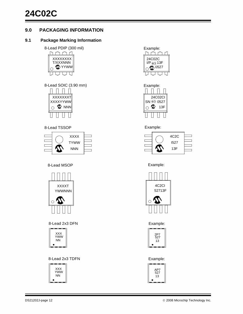
9.0 PACKAGING INFORMATION
9.1 Package Marking Information
XXXXXXXXT/XXXNNN
YYWW
8-Lead PDIP (300 mil) Example:
8-Lead SOIC (3.90 mm) Example:
XXXXXXXTXXXXYYWW
NNN
8-Lead TSSOP Example:
24C02CI/P 13F
0527
24C02CISN 0527
13F
8-Lead MSOP Example:
XXXX
TYWW
NNN
4C2C
I527
13F
XXXXTYWWNNN
3e
3e
8-Lead 2x3 DFN
XXXYWWNN
2P752713
Example:
4C2CI52713F
8-Lead 2x3 TDFN
XXXYWWNN
AP752713
Example:
DS21202J-page 12 © 2008 Microchip Technology Inc.
24C02C
Part Number
1st Line Marking Codes
TSSOP MSOPDFN TDFN
I Temp. E Temp. I Temp. E Temp.
24C02C 4C2C 4C2CT 2P7 2P8 AP7 AP8Note: T = Temperature grade (I, E)
Legend: XX...X Part number or part number codeT Temperature (I, E)Y Year code (last digit of calendar year)YY Year code (last 2 digits of calendar year)WW Week code (week of January 1 is week ‘01’)NNN Alphanumeric traceability code (2 characters for small packages)
Pb-free JEDEC designator for Matte Tin (Sn)
Note: For very small packages with no room for the Pb-free JEDEC designator , the marking will only appear on the outer carton or reel label.
Note: In the event the full Microchip part number cannot be marked on one line, it willbe carried over to the next line, thus limiting the number of availablecharacters for customer-specific information.
3e
3e
Note: Please visit www.microchip.com/Pbfree for the latest information on Pb-free conversion.
*Standard OTP marking consists of Microchip part number, year code, week code, and traceability code.
© 2008 Microchip Technology Inc. DS21202J-page 13
24C02C
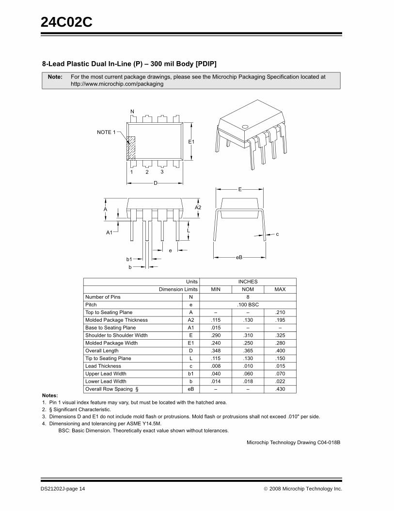
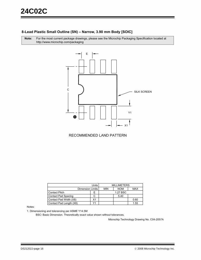
���������� ���������� ������������� ����������
�������� ������ �!"�����#�$�%��&"��'��� ��(�)"&�'"!&�)�����&�#�*�&��&�����&���#������� +������%����&�,����&��!&���-� ��'��!��!�����#�.��#��&�����"#��'�#�%��!����&"!��!����#�%��!����&"!��!�!������&��$���#�����/����!�#���� ��'��!��������#�&���������������.�0������
1�,2�1�!�����'��!���� ���&��������$��&� ��"��!�*��*�&�"&�&������!�
����� 3�&���'!&��"��&����4����#�*���!(�����!��!���&��������������4�����������%���&������&�#��&��&&�255***�'��������'5���4�����
6��&! �7,8.���'��!���9�'�&! ��7 7:� ��;
7"')��%����! 7 <��&�� � �����1�, ��&����&��������� � = = ������#�#����4���� ���4��!! �� ���� ��-� ����1�!��&����&��������� �� ���� = =��"�#��&���"�#��>�#&� . ���� �-�� �-����#�#����4����>�#&� .� ���� ���� ��<�: �����9���&� � �-�< �-?� ���� ���&����&��������� 9 ���� ��-� ����9��#� ���4��!! � ���< ���� ����6����9��#�>�#&� )� ���� ��?� ����9*��9��#�>�#&� ) ���� ���< ����: ������*����������+ �1 = = ��-�
N
E1
NOTE 1
D
1 2 3
A
A1
A2
L
b1b
e
E
eB
c
������� ������� ��*��� ,�����<1
DS21202J-page 14 © 2008 Microchip Technology Inc.
24C02C
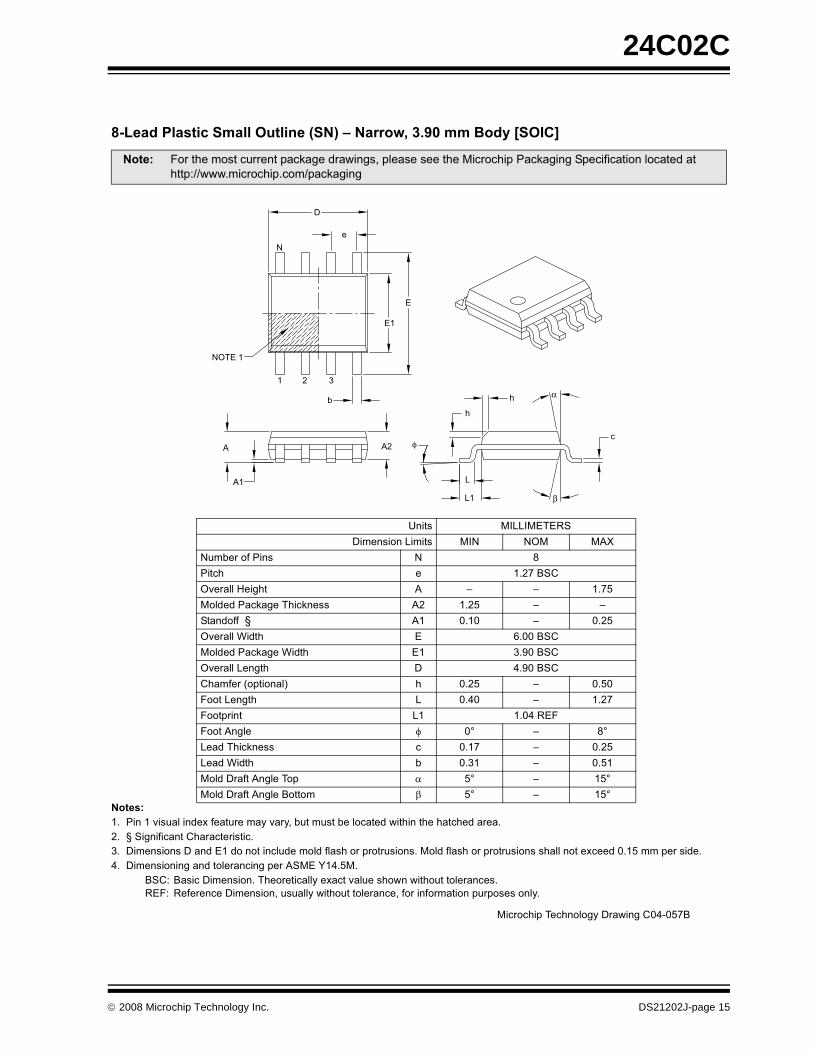
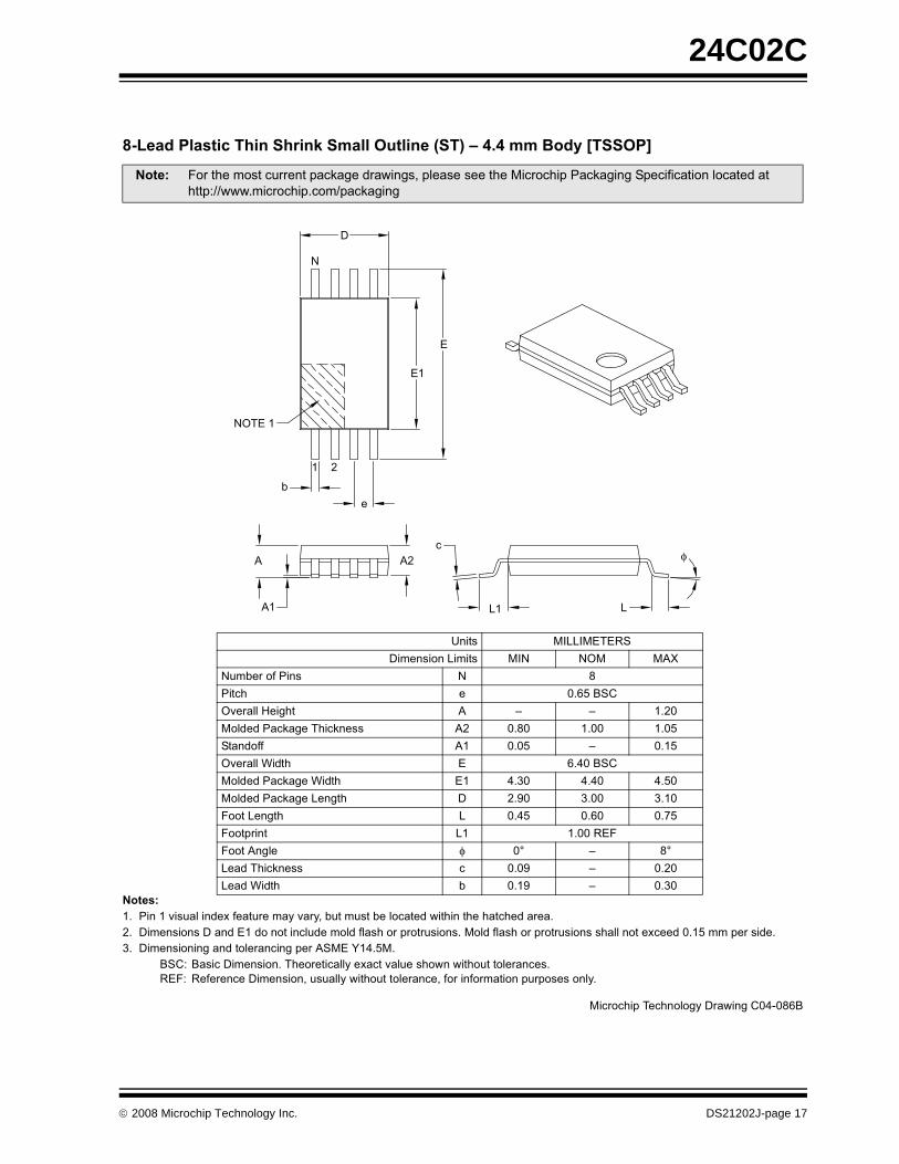
���������� �� ���!�� ���� �������""�#$��%&����������� !�'�
�������� ������ �!"�����#�$�%��&"��'��� ��(�)"&�'"!&�)�����&�#�*�&����&�����&���#������� +������%����&�,����&��!&���-� ��'��!��!�����#�.��#��&�����"#��'�#�%��!����&"!��!����#�%��!����&"!��!�!������&��$���#������''����!�#���� ��'��!��������#�&���������������.�0������
1�,2 1�!�����'��!���� ���&��������$��&� ��"��!�*��*�&�"&�&������!��.32 ��%��������'��!��(�"!"�����*�&�"&�&������(�%���%'�&����"�!�!�����
����� 3�&���'!&��"��&����4����#�*���!(�����!��!���&��������������4�����������%���&������&�#��&��&&�255***�'��������'5���4�����
6��&! ��99��. .����'��!���9�'�&! ��7 7:� ��;
7"')��%����! 7 <��&�� � �����1�,: �����8����& � = = ������#�#����4���� ���4��!! �� ���� = =�&��#%%��+ �� ���� = ����: �����>�#&� . ?����1�,��#�#����4����>�#&� .� -����1�,: �����9���&� � �����1�,,��'%��@�&����A � ���� = ����3&�9���&� 9 ���� = ����3&���& 9� ������.33&������ � �B = <B9��#� ���4��!! � ���� = ����9��#�>�#&� ) ��-� = ������#���%&������� � � �B = ��B��#���%&�������1&&' � �B = ��B
D
Ne
E
E1
NOTE 1
1 2 3
b
A
A1
A2
L
L1
c
h
h
φ
β
α
������� ������� ��*��� ,������1
© 2008 Microchip Technology Inc. DS21202J-page 15
24C02C
���������� �� ���!�� ���� �������""�#$��%&����������� !�'�
����� 3�&���'!&��"��&����4����#�*���!(�����!��!���&��������������4�����������%���&������&�#��&��&&�255***�'��������'5���4�����
DS21202J-page 16 © 2008 Microchip Technology Inc.
24C02C
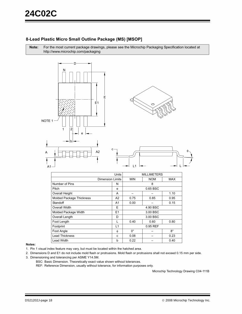
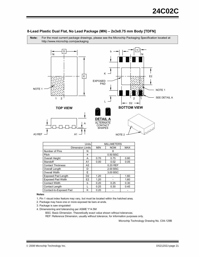
���������� ��() �� )" �*� ���!�� ���� (����+%+����������( !�
�������� ������ �!"�����#�$�%��&"��'��� ��(�)"&�'"!&�)�����&�#�*�&����&�����&���#������� ��'��!��!�����#�.��#��&�����"#��'�#�%��!����&"!��!����#�%��!����&"!��!�!������&��$���#������''����!�#��-� ��'��!��������#�&���������������.�0������
1�,2 1�!�����'��!���� ���&��������$��&� ��"��!�*��*�&�"&�&������!��.32 ��%��������'��!��(�"!"�����*�&�"&�&������(�%���%'�&����"�!�!�����
����� 3�&���'!&��"��&����4����#�*���!(�����!��!���&��������������4�����������%���&������&�#��&��&&�255***�'��������'5���4�����
6��&! ��99��. .����'��!���9�'�&! ��7 7:� ��;
7"')��%����! 7 <��&�� � ��?��1�,: �����8����& � = = ������#�#����4���� ���4��!! �� ��<� ���� �����&��#%%� �� ���� = ����: �����>�#&� . ?����1�,��#�#����4����>�#&� .� ��-� ���� ������#�#����4����9���&� � ���� -��� -���3&�9���&� 9 ���� ��?� ����3&���& 9� ������.33&������ � �B = <B9��#� ���4��!! � ���� = ����9��#�>�#&� ) ���� = ��-�
D
N
E
E1
NOTE 1
1 2
be
cA
A1
A2
L1 L
φ
������� ������� ��*��� ,����<?1
© 2008 Microchip Technology Inc. DS21202J-page 17
24C02C
���������� ��, �"�� ���!�� �����*�-���, ���, !�
�������� ������ �!"�����#�$�%��&"��'��� ��(�)"&�'"!&�)�����&�#�*�&����&�����&���#������� ��'��!��!�����#�.��#��&�����"#��'�#�%��!����&"!��!����#�%��!����&"!��!�!������&��$���#������''����!�#��-� ��'��!��������#�&���������������.�0������
1�,2 1�!�����'��!���� ���&��������$��&� ��"��!�*��*�&�"&�&������!��.32 ��%��������'��!��(�"!"�����*�&�"&�&������(�%���%'�&����"�!�!�����
����� 3�&���'!&��"��&����4����#�*���!(�����!��!���&��������������4�����������%���&������&�#��&��&&�255***�'��������'5���4�����
6��&! ��99��. .����'��!���9�'�&! ��7 7:� ��;
7"')��%����! 7 <��&�� � ��?��1�,: �����8����& � = = ������#�#����4���� ���4��!! �� ���� ��<� �����&��#%%� �� ���� = ����: �����>�#&� . �����1�,��#�#����4����>�#&� .� -����1�,: �����9���&� � -����1�,3&�9���&� 9 ���� ��?� ��<�3&���& 9� ������.33&������ � �B = <B9��#� ���4��!! � ���< = ���-9��#�>�#&� ) ���� = ����
D
N
E
E1
NOTE 1
1 2e
b
A
A1
A2c
L1 L
φ
������� ������� ��*��� ,������1
DS21202J-page 18 © 2008 Microchip Technology Inc.
24C02C
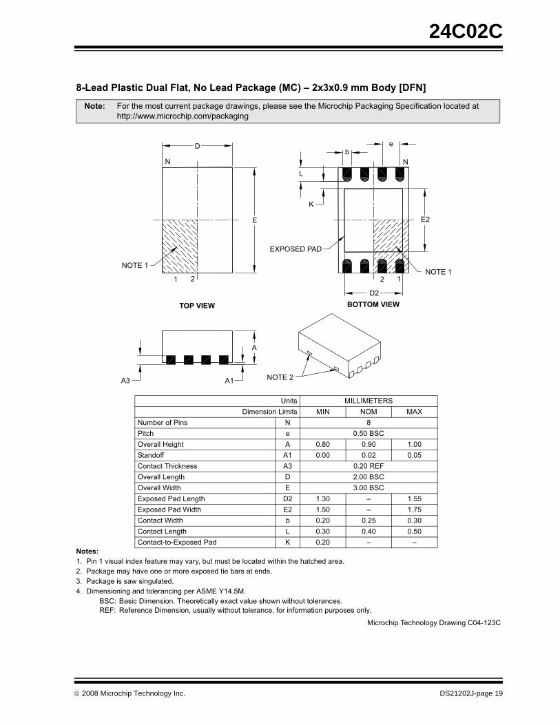
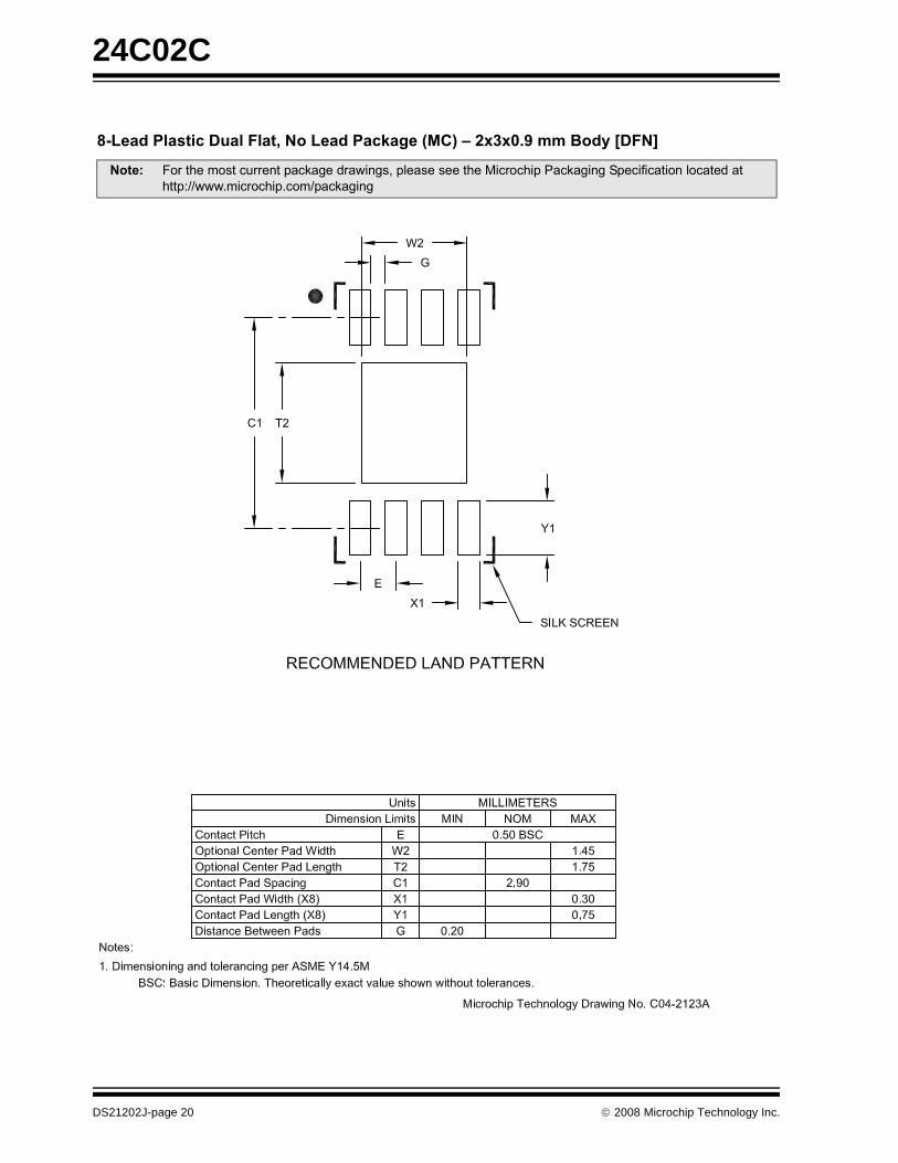
���������� ������.��$�����������*�-���,'����/0�0�%&�����������.��
�������� ������ �!"�����#�$�%��&"��'��� ��(�)"&�'"!&�)�����&�#�*�&����&�����&���#������� ���4����'����� ������'���$�!�#�&���)�!��&���#!�-� ���4�����!�!�*�!���"��&�#��� ��'��!��������#�&���������������.�0������
1�,2 1�!�����'��!���� ���&��������$��&� ��"��!�*��*�&�"&�&������!��.32 ��%��������'��!��(�"!"�����*�&�"&�&������(�%���%'�&����"�!�!�����
����� 3�&���'!&��"��&����4����#�*���!(�����!��!���&��������������4�����������%���&������&�#��&��&&�255***�'��������'5���4�����
6��&! ��99��. .����'��!���9�'�&! ��7 7:� ��;
7"')��%����! 7 <��&�� � �����1�,: �����8����& � ��<� ���� �����&��#%%� �� ���� ���� ����,�&��&� ���4��!! �- ������.3: �����9���&� � �����1�,: �����>�#&� . -����1�,.$�!�#���#�9���&� �� ��-� = ����.$�!�#���#�>�#&� .� ���� = ����,�&��&�>�#&� ) ���� ���� ��-�,�&��&�9���&� 9 ��-� ���� ����,�&��&�&�.$�!�#���# C ���� = =
D
N
E
NOTE 1
1 2
EXPOSED PAD
NOTE 12 1
D2
K
L
E2
N
eb
A3 A1
A
NOTE 2
BOTTOM VIEWTOP VIEW
������� ������� ��*��� ,�����-,
© 2008 Microchip Technology Inc. DS21202J-page 19
24C02C
���������� ������.��$�����������*�-���,'����/0�0�%&�����������.��
����� 3�&���'!&��"��&����4����#�*���!(�����!��!���&��������������4�����������%���&������&�#��&��&&�255***�'��������'5���4�����
DS21202J-page 20 © 2008 Microchip Technology Inc.
24C02C
���������� ������.��$�����������*�-���,�����/0�0�%12����������(�.��
����� 3�&���'!&��"��&����4����#�*���!(�����!��!���&��������������4�����������%���&������&�#��&��&&�255***�'��������'5���4�����
© 2008 Microchip Technology Inc. DS21202J-page 21

24C02C
���������� ������.��$�����������*�-���,�����/0�0�%12����������(�.��
����� 3�&���'!&��"��&����4����#�*���!(�����!��!���&��������������4�����������%���&������&�#��&��&&�255***�'��������'5���4�����
DS21202J-page 22 © 2008 Microchip Technology Inc.
24C02C
APPENDIX A: REVISION HISTORY
Revision DCorrections to Section 1.0, Electrical Characteristics.
Revision EAdded DFN package.
Revision F (02/2007)Revised Features section; Section 1.0 revised Ambienttemperature; Revised Tables 1-1, 1-2, (removed com-mercial temp); Revised Table 2-1; Replaced On-lineSupport page; Replaced Package Drawings; RevisedProduct ID section.
Revision G (03/2007)Replaced Package Drawings (Rev. AM).
Revision H (04/2008) Replaced Package Drawings; Added TDFN package;Revised Product ID section.
Revision J (08/2008)Corrections to Table 1-1, DC Characteristics; UpdatedTable 1-2, AC Characteristics; Revised Figure 1-1;Updated Package Drawings.
© 2008 Microchip Technology Inc. DS21202J-page 23
24C02C
NOTES:DS21202J-page 24 © 2008 Microchip Technology Inc.
24C02C
THE MICROCHIP WEB SITEMicrochip provides online support via our WWW site atwww.microchip.com. This web site is used as a meansto make files and information easily available tocustomers. Accessible by using your favorite Internetbrowser, the web site contains the followinginformation:
• Product Support – Data sheets and errata, application notes and sample programs, design resources, user’s guides and hardware support documents, latest software releases and archived software
• General Technical Support – Frequently Asked Questions (FAQ), technical support requests, online discussion groups, Microchip consultant program member listing
• Business of Microchip – Product selector and ordering guides, latest Microchip press releases, listing of seminars and events, listings of Microchip sales offices, distributors and factory representatives
CUSTOMER CHANGE NOTIFICATION SERVICEMicrochip’s customer notification service helps keepcustomers current on Microchip products. Subscriberswill receive e-mail notification whenever there arechanges, updates, revisions or errata related to aspecified product family or development tool of interest.
To register, access the Microchip web site atwww.microchip.com, click on Customer ChangeNotification and follow the registration instructions.
CUSTOMER SUPPORTUsers of Microchip products can receive assistancethrough several channels:
• Distributor or Representative• Local Sales Office• Field Application Engineer (FAE)• Technical Support• Development Systems Information Line
Customers should contact their distributor,representative or field application engineer (FAE) forsupport. Local sales offices are also available to helpcustomers. A listing of sales offices and locations isincluded in the back of this document.
Technical support is available through the web siteat: http://support.microchip.com
© 2008 Microchip Technology Inc. DS21202J-page 25

24C02C
READER RESPONSEIt is our intention to provide you with the best documentation possible to ensure successful use of your Microchip prod-uct. If you wish to provide your comments on organization, clarity, subject matter, and ways in which our documentationcan better serve you, please FAX your comments to the Technical Publications Manager at (480) 792-4150.
Please list the following information, and use this outline to provide us with your comments about this document.
To: Technical Publications Manager
RE: Reader ResponseTotal Pages Sent ________
From: Name
CompanyAddressCity / State / ZIP / Country
Telephone: (_______) _________ - _________
Application (optional):
Would you like a reply? Y N
Device: Literature Number:
Questions:
FAX: (______) _________ - _________
DS21202J24C02C
1. What are the best features of this document?
2. How does this document meet your hardware and software development needs?
3. Do you find the organization of this document easy to follow? If not, why?
4. What additions to the document do you think would enhance the structure and subject?
5. What deletions from the document could be made without affecting the overall usefulness?
6. Is there any incorrect or misleading information (what and where)?
7. How would you improve this document?
DS21202J-page 26 © 2008 Microchip Technology Inc.
24C02C
PRODUCT IDENTIFICATION SYSTEMTo order or obtain information, e.g., on pricing or delivery, refer to the factory or the listed sales office.
PART NO. X /XX
PackageTemperatureRange
Device
Device: 24C02C: 2K I2C™ Serial EEPROM
24C02CT: 2K I2C™ Serial EEPROM (Tape and Reel)
Temperature Range:
I = -40°C to +85°CE = -40°C to +125°C
Package: P = Plastic DIP (300 mil Body), 8-leadSN = Plastic SOIC, (3.90 mm Body), 8-leadST = TSSOP (4.4 mm Body), 8-leadMS = Plastic Micro Small Outline (MSOP), 8-leadMC = Plastic Dual Flat (DFN), No lead package,
2x3 mm body, 8-leadMNY(1) = Plastic Dual Flat (TDFN), No lead package,
2x3 mm body, 8-lead
Examples:
a) 24C02C-I/P: Industrial Temperature,PDIP Package
b) 24C02C-E/SN: Extended Temperature,SOIC Package
c) 24C02C-I/MNY: Industrial Temperature,2x3 TDFN Package
Note 1: “Y” indicates a Nickel, Palladium, Gold (NiPdAu) finish.
© 2008 Microchip Technology Inc. DS21202J-page 27

24C02C
NOTES:DS21202J-page 28 © 2008 Microchip Technology Inc.
Note the following details of the code protection feature on Microchip devices:• Microchip products meet the specification contained in their particular Microchip Data Sheet.
• Microchip believes that its family of products is one of the most secure families of its kind on the market today, when used in the intended manner and under normal conditions.
• There are dishonest and possibly illegal methods used to breach the code protection feature. All of these methods, to our knowledge, require using the Microchip products in a manner outside the operating specifications contained in Microchip’s Data Sheets. Most likely, the person doing so is engaged in theft of intellectual property.
• Microchip is willing to work with the customer who is concerned about the integrity of their code.
• Neither Microchip nor any other semiconductor manufacturer can guarantee the security of their code. Code protection does not mean that we are guaranteeing the product as “unbreakable.”
Code protection is constantly evolving. We at Microchip are committed to continuously improving the code protection features of ourproducts. Attempts to break Microchip’s code protection feature may be a violation of the Digital Millennium Copyright Act. If such actsallow unauthorized access to your software or other copyrighted work, you may have a right to sue for relief under that Act.
Information contained in this publication regarding deviceapplications and the like is provided only for your convenienceand may be superseded by updates. It is your responsibility toensure that your application meets with your specifications.MICROCHIP MAKES NO REPRESENTATIONS ORWARRANTIES OF ANY KIND WHETHER EXPRESS ORIMPLIED, WRITTEN OR ORAL, STATUTORY OROTHERWISE, RELATED TO THE INFORMATION,INCLUDING BUT NOT LIMITED TO ITS CONDITION,QUALITY, PERFORMANCE, MERCHANTABILITY ORFITNESS FOR PURPOSE. Microchip disclaims all liabilityarising from this information and its use. Use of Microchipdevices in life support and/or safety applications is entirely atthe buyer’s risk, and the buyer agrees to defend, indemnify andhold harmless Microchip from any and all damages, claims,suits, or expenses resulting from such use. No licenses areconveyed, implicitly or otherwise, under any Microchipintellectual property rights.
© 2008 Microchip Technology Inc.
Trademarks
The Microchip name and logo, the Microchip logo, Accuron, dsPIC, KEELOQ, KEELOQ logo, MPLAB, PIC, PICmicro, PICSTART, rfPIC and SmartShunt are registered trademarks of Microchip Technology Incorporated in the U.S.A. and other countries.
FilterLab, Linear Active Thermistor, MXDEV, MXLAB, SEEVAL, SmartSensor and The Embedded Control Solutions Company are registered trademarks of Microchip Technology Incorporated in the U.S.A.
Analog-for-the-Digital Age, Application Maestro, CodeGuard, dsPICDEM, dsPICDEM.net, dsPICworks, dsSPEAK, ECAN, ECONOMONITOR, FanSense, In-Circuit Serial Programming, ICSP, ICEPIC, Mindi, MiWi, MPASM, MPLAB Certified logo, MPLIB, MPLINK, mTouch, PICkit, PICDEM, PICDEM.net, PICtail, PIC32 logo, PowerCal, PowerInfo, PowerMate, PowerTool, REAL ICE, rfLAB, Select Mode, Total Endurance, UNI/O, WiperLock and ZENA are trademarks of Microchip Technology Incorporated in the U.S.A. and other countries.
SQTP is a service mark of Microchip Technology Incorporated in the U.S.A.
All other trademarks mentioned herein are property of their respective companies.
© 2008, Microchip Technology Incorporated, Printed in the U.S.A., All Rights Reserved.
Printed on recycled paper.
DS21202J-page 29
Microchip received ISO/TS-16949:2002 certification for its worldwide headquarters, design and wafer fabrication facilities in Chandler and Tempe, Arizona; Gresham, Oregon and design centers in California and India. The Company’s quality system processes and procedures are for its PIC® MCUs and dsPIC® DSCs, KEELOQ® code hopping devices, Serial EEPROMs, microperipherals, nonvolatile memory and analog products. In addition, Microchip’s quality system for the design and manufacture of development systems is ISO 9001:2000 certified.
DS21202J-page 30 © 2008 Microchip Technology Inc.
AMERICASCorporate Office2355 West Chandler Blvd.Chandler, AZ 85224-6199Tel: 480-792-7200 Fax: 480-792-7277Technical Support: http://support.microchip.comWeb Address: www.microchip.comAtlantaDuluth, GA Tel: 678-957-9614 Fax: 678-957-1455BostonWestborough, MA Tel: 774-760-0087 Fax: 774-760-0088ChicagoItasca, IL Tel: 630-285-0071 Fax: 630-285-0075DallasAddison, TX Tel: 972-818-7423 Fax: 972-818-2924DetroitFarmington Hills, MI Tel: 248-538-2250Fax: 248-538-2260KokomoKokomo, IN Tel: 765-864-8360Fax: 765-864-8387Los AngelesMission Viejo, CA Tel: 949-462-9523 Fax: 949-462-9608Santa ClaraSanta Clara, CA Tel: 408-961-6444Fax: 408-961-6445TorontoMississauga, Ontario, CanadaTel: 905-673-0699 Fax: 905-673-6509
ASIA/PACIFICAsia Pacific OfficeSuites 3707-14, 37th FloorTower 6, The GatewayHarbour City, KowloonHong KongTel: 852-2401-1200Fax: 852-2401-3431Australia - SydneyTel: 61-2-9868-6733Fax: 61-2-9868-6755China - BeijingTel: 86-10-8528-2100 Fax: 86-10-8528-2104China - ChengduTel: 86-28-8665-5511Fax: 86-28-8665-7889China - Hong Kong SARTel: 852-2401-1200 Fax: 852-2401-3431China - NanjingTel: 86-25-8473-2460Fax: 86-25-8473-2470China - QingdaoTel: 86-532-8502-7355Fax: 86-532-8502-7205China - ShanghaiTel: 86-21-5407-5533 Fax: 86-21-5407-5066China - ShenyangTel: 86-24-2334-2829Fax: 86-24-2334-2393China - ShenzhenTel: 86-755-8203-2660 Fax: 86-755-8203-1760China - WuhanTel: 86-27-5980-5300Fax: 86-27-5980-5118China - XiamenTel: 86-592-2388138 Fax: 86-592-2388130China - XianTel: 86-29-8833-7252Fax: 86-29-8833-7256China - ZhuhaiTel: 86-756-3210040 Fax: 86-756-3210049
ASIA/PACIFICIndia - BangaloreTel: 91-80-4182-8400 Fax: 91-80-4182-8422India - New DelhiTel: 91-11-4160-8631Fax: 91-11-4160-8632India - PuneTel: 91-20-2566-1512Fax: 91-20-2566-1513Japan - YokohamaTel: 81-45-471- 6166 Fax: 81-45-471-6122Korea - DaeguTel: 82-53-744-4301Fax: 82-53-744-4302Korea - SeoulTel: 82-2-554-7200Fax: 82-2-558-5932 or 82-2-558-5934Malaysia - Kuala LumpurTel: 60-3-6201-9857Fax: 60-3-6201-9859Malaysia - PenangTel: 60-4-227-8870Fax: 60-4-227-4068Philippines - ManilaTel: 63-2-634-9065Fax: 63-2-634-9069SingaporeTel: 65-6334-8870Fax: 65-6334-8850Taiwan - Hsin ChuTel: 886-3-572-9526Fax: 886-3-572-6459Taiwan - KaohsiungTel: 886-7-536-4818Fax: 886-7-536-4803Taiwan - TaipeiTel: 886-2-2500-6610 Fax: 886-2-2508-0102Thailand - BangkokTel: 66-2-694-1351Fax: 66-2-694-1350
EUROPEAustria - WelsTel: 43-7242-2244-39Fax: 43-7242-2244-393Denmark - CopenhagenTel: 45-4450-2828 Fax: 45-4485-2829France - ParisTel: 33-1-69-53-63-20 Fax: 33-1-69-30-90-79Germany - MunichTel: 49-89-627-144-0 Fax: 49-89-627-144-44Italy - Milan Tel: 39-0331-742611 Fax: 39-0331-466781Netherlands - DrunenTel: 31-416-690399 Fax: 31-416-690340Spain - MadridTel: 34-91-708-08-90Fax: 34-91-708-08-91UK - WokinghamTel: 44-118-921-5869Fax: 44-118-921-5820
WORLDWIDE SALES AND SERVICE
01/02/08
![Τα Θεμελιώδη Θεωρήματα του Piero Sraffa και η ......And new philosophy calls all in doubt, […] ’Tis all in pieces, all coherence gone, All just supply,](https://static.fdocument.org/doc/165x107/5fd4dd5d839bba543d442528/-piero-sraffa-.jpg)


![Πού είναι ο άρης [all]](https://static.fdocument.org/doc/165x107/568c34b61a28ab023591802a/-all568c34b61a28ab023591802a.jpg)