
WHITE PAPER SERIES / EDITION 1 BUSINESS...
12
AUTOIDLABS-WP-HARDWARE-010 System Modeling and Simulation of RFID Yifeng Han, Hao Min Auto-ID Labs at Fudan University, Shanghai, P. R. China, 200433 hanyf @ fudan.edu.cn, hmin @ fudan.edu.cn www.autoidlabs.org BUSINESS PROCESSES & APPLICATIONS SOFTWARE & NETWORK HARDWARE WHITE PAPER SERIES / EDITION 1 Copyright © September 2005
-
Upload
nguyennguyet -
Category
Documents
-
view
218 -
download
1
Transcript of WHITE PAPER SERIES / EDITION 1 BUSINESS...
AUTOIDLABS-WP-HARDWARE-010
System Modeling andSimulation of RFIDYifeng Han, Hao Min
Auto-ID Labs at Fudan University,Shanghai, P. R. China, 200433
[email protected], [email protected]
BU
SIN
ESS
PR
OCE
SS
ES &
AP
PLI
CAT
ION
SS
OFT
WA
RE
& N
ETW
OR
KH
AR
DW
AR
EWHITE PAPER SERIES / EDITION 1
Copyright © September 2005
1 System Modeling and Simulating of RFID
AbstractA system simulation environment in Matlab/Simulink of RFID is constructed in this paper. Special attention is emphasized on the analog/RF circuit. Negative effects are concerned in the system model, such as phase noise of the local oscillator, TX-RX coupling, reflection of the environment, AWGN noise, DC offset, I/Q mis-match, etc. Performance of the whole system can be evaluated by changing the coding method, parameters of building blocks, and operation distance. Finally, some simulation results are presented in this paper.
1. Introduction
UHF RFID system can be divided to two parts, readers and tags. Generally, an RFID system contains several readers and a large amount of tags in practical application. The collision problems of both tags and readers are resolved in the arithmetic [1] and MAC protocol [2].
For a simple analysis, a single reader and a single tag bi-direc-tional communication can be investigated to reveal the physical parameters. The communication link is half duplex, reader to tag and then tag to reader. In forward link, reader sends a modulated carrier to tags and powers up the tags. The tags arbitrate their state and determine which tag responds to reader. In return link, reader sends an continues wave carrier, tag receives the carrier for power supply and backscatters by changing the reflection coeffi-cients of antenna. In such a way, data is sent to reader from tag.
Readers should be designed to comply the local frequency regu-latory in transmitter. To detect the backscatter signals from tag, a relative high sensitivity (-85dBm e.g.) is chosen at a given bit error rate (BER=1e-3, e. g.).
This paper is to construct a system model of the forward link and return link.. In the simulation, protocol of EPC Class 1 Genera-tion 2 [3] is used as an example. If a few changes at coding, data rate, reflection method etc. are made, it is very convenient to simulate the system performance under other protocols. In sec-tion 2, a brief description of system model and system model in Matlab/Simulink is introduced. Section 3 describes the Models of building blocks of RFID by transmitter, tags, wireless channel and receiver respectively. Section 4 deals with the simulation results of transmitter, tags and receiver. Finally, section 5 presents the discussions and conclusions.
2 System Modeling and Simulating of RFID
2. System Model of RFID
RFID system can be partitioned into three simple blocks, reader, tag, and wireless channel, as Figure 1. Transmitter and receiver in Figure 1 are the front end of reader. To get the system performance and compatible for multi-protocol operation, signal-processing blocks are included in system model except the commands in protocols.
TransmitterTag
Wireless Channeld
Receiver
Reader
Fig. 1: General building blocks of RFID
Figure 2 is the simulation environment of transmitter in Simulink. The performance such as output spectrum can be seen by addi-tional signal processing using Matlab. In forward link, it is criti-cal to see whether the transmitting signal is under the frequency mask of the localregulation. Therefore raised cosine filter, Hilbert transform, DAC (quantization error) and filter, PLL, non-ideal mixer and high power amplifier etc. are added. The transmission types can be selected among SSB, DSB and continuous wave carrier by switching the manual switches in Figure 2.
Figure 3 is the simulation environment of return link. The trans-mitter sends a continuous carrier to power up tag. The free space is modeled by pass loss with phase changing due to distance between reader and tag. AWGN channel is added to model the noise sources from space. Another source of receiving power is the direct coupling from TX to RX. It is modeled by a proper gain and
phase delay. The tag is modeled by coding method, antenna gain, and percent of reflection. The receiver includes band pass filter, LNA, Mixer, AC coupling, channel select filter and the variable gain stages. The BER performance can be seen by comparing the re-ceived and down converted signal with the data tag backscattered
SourceCoding
Raise CosineHilbert
DACSmooth Filter
IQ Imbalance DSB/SSB/CW Switch
PLL
UpConversion
HPA/BPF/ANTAData
Processing
Fig. 2: Transmitter simulation environment in Simulink
3 System Modeling and Simulating of RFID
PLL
Transmitter
Free Space
Receiver
DirectCoupling
Tag Reflection
Fig. 3: Simulation of return link
3. Models of the Building Blocks of RFID System
3.1 Model of TransmitterThe architecture of transmitter is chosen to be I/Q-branches for the reasons of SSB transmission and different modulation meth-ods such as ASK or PSK.
The simulation in this paper is based on [3]. The coding for for-ward link is Manchester coding. The transmitter should fulfill the protocol and support the DSB or SSB transmitting for forward link, send an un-modulated carrier for return link. Figure 4 gives the configurations of transmitter for different modulations.
Data
Rasied CosineFilter Ilo
Qlo
DSB
0
Data
Raised CosineFilter
HilbertTransform
Ilo
Qlo
SSB
1
Ilo
Qlo
UnmodulatedCarrier
0
Fig. 4: Configurations for SSB, DSB and return link
3.1.1 CodingThe protocol this paper based on using Manchester coding for forward link, FM0 and Manchester subcarrier coding for return link [3]. The power spectral density of Manchester subcarrier is differ-ent with Manchester since a DC component is added by the asym-metric probability of two levels.
BER is introduced to evaluate the performance of a digital com-munication system. In forward link, the CNR is large enough for a tag to demodulate data by envelope detector. The tag reflects the incident power, and the reflect power is very weak for a pas-sive tag since it can only send the return data through changing RCS(what is RCS?, Please indicate) which is very small. If most of the power were reflected, the tag would not work. If less power were reflected, reader would not reach a high sensitivity physi-cally. The SNR requisition under a given BER for some modulation type is listed in Table 1. A BER of 1e-3 is chosen for RFID system in some products.
4 System Modeling and Simulating of RFID
BER 1e-3 1e-5 1e-7
PSK 6.8dB 9.6dB 11.4dB
FM0/Manchester subcarrier 9.8dB 12.6dB 14.4dB
FSK 11.0dB 13.4dB 14.9dB
ASK 12.6dB 15.2dB 18.6dB
Table 1: SNR requisition of different modulation types
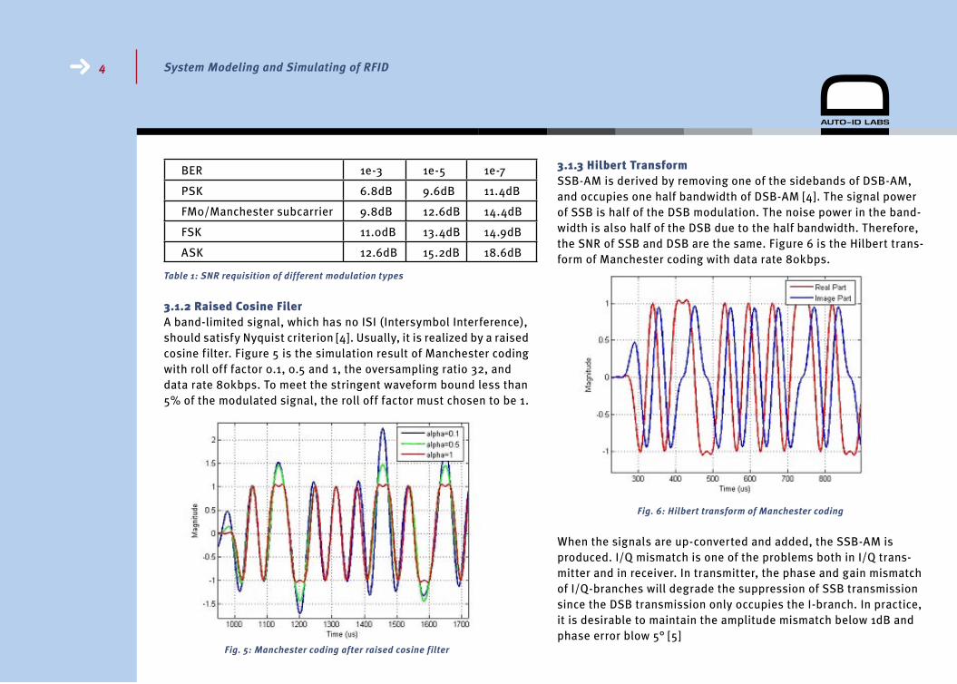
3.1.2 Raised Cosine FilerA band-limited signal, which has no ISI (Intersymbol Interference), should satisfy Nyquist criterion [4]. Usually, it is realized by a raised cosine filter. Figure 5 is the simulation result of Manchester coding with roll off factor 0.1, 0.5 and 1, the oversampling ratio 32, and data rate 80kbps. To meet the stringent waveform bound less than 5% of the modulated signal, the roll off factor must chosen to be 1.
Fig. 5: Manchester coding after raised cosine filter
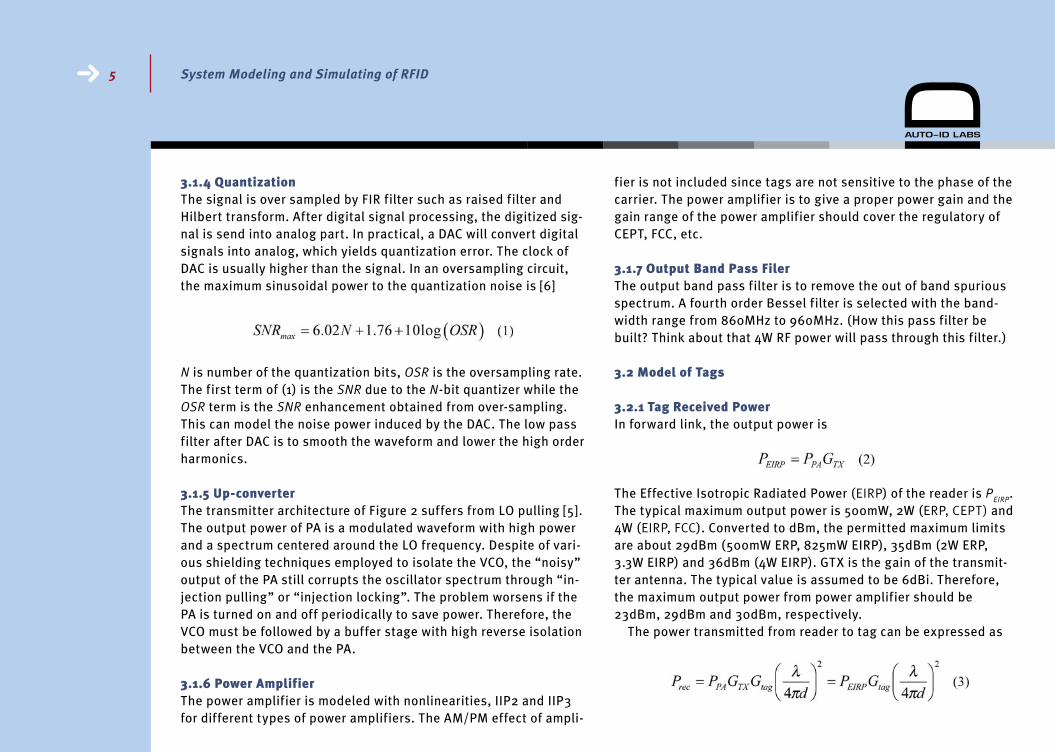
3.1.3 Hilbert TransformSSB-AM is derived by removing one of the sidebands of DSB-AM, and occupies one half bandwidth of DSB-AM [4]. The signal power of SSB is half of the DSB modulation. The noise power in the band-width is also half of the DSB due to the half bandwidth. Therefore, the SNR of SSB and DSB are the same. Figure 6 is the Hilbert trans-form of Manchester coding with data rate 80kbps.
Fig. 6: Hilbert transform of Manchester coding
When the signals are up-converted and added, the SSB-AM is produced. I/Q mismatch is one of the problems both in I/Q trans-mitter and in receiver. In transmitter, the phase and gain mismatch of I/Q-branches will degrade the suppression of SSB transmission since the DSB transmission only occupies the I-branch. In practice, it is desirable to maintain the amplitude mismatch below 1dB and phase error blow 5° [5]
5 System Modeling and Simulating of RFID
3.1.4 QuantizationThe signal is over sampled by FIR filter such as raised filter and Hilbert transform. After digital signal processing, the digitized sig-nal is send into analog part. In practical, a DAC will convert digital signals into analog, which yields quantization error. The clock of DAC is usually higher than the signal. In an oversampling circuit, the maximum sinusoidal power to the quantization noise is [6]
N is number of the quantization bits, OSR is the oversampling rate. The first term of (1) is the SNR due to the N-bit quantizer while the OSR term is the SNR enhancement obtained from over-sampling. This can model the noise power induced by the DAC. The low pass filter after DAC is to smooth the waveform and lower the high order harmonics.
3.1.5 Up-converterThe transmitter architecture of Figure 2 suffers from LO pulling [5]. The output power of PA is a modulated waveform with high power and a spectrum centered around the LO frequency. Despite of vari-ous shielding techniques employed to isolate the VCO, the “noisy” output of the PA still corrupts the oscillator spectrum through “in-jection pulling” or “injection locking”. The problem worsens if the PA is turned on and off periodically to save power. Therefore, the VCO must be followed by a buffer stage with high reverse isolation between the VCO and the PA.
3.1.6 Power AmplifierThe power amplifier is modeled with nonlinearities, IIP2 and IIP3 for different types of power amplifiers. The AM/PM effect of ampli-
fier is not included since tags are not sensitive to the phase of the carrier. The power amplifier is to give a proper power gain and the gain range of the power amplifier should cover the regulatory of CEPT, FCC, etc.
3.1.7 Output Band Pass FilerThe output band pass filter is to remove the out of band spurious spectrum. A fourth order Bessel filter is selected with the band-width range from 860MHz to 960MHz. (How this pass filter be built? Think about that 4W RF power will pass through this filter.)
3.2 Model of Tags
3.2.1 Tag Received PowerIn forward link, the output power is
The Effective Isotropic Radiated Power (EIRP) of the reader is PEIRP
. The typical maximum output power is 500mW, 2W (ERP, CEPT) and 4W (EIRP, FCC). Converted to dBm, the permitted maximum limits are about 29dBm (500mW ERP, 825mW EIRP), 35dBm (2W ERP, 3.3W EIRP) and 36dBm (4W EIRP). GTX is the gain of the transmit-ter antenna. The typical value is assumed to be 6dBi. Therefore, the maximum output power from power amplifier should be 23dBm, 29dBm and 30dBm, respectively.
The power transmitted from reader to tag can be expressed as
6 System Modeling and Simulating of RFID
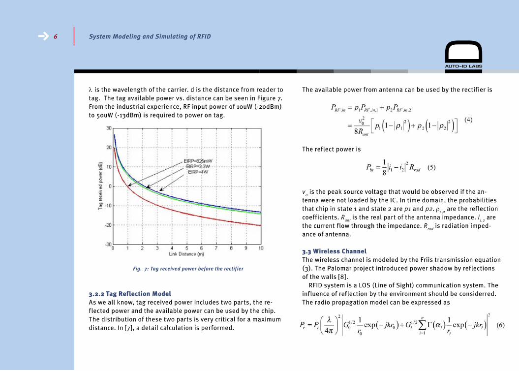
λ is the wavelength of the carrier. d is the distance from reader to tag. The tag available power vs. distance can be seen in Figure 7. From the industrial experience, RF input power of 10uW (-20dBm) to 50uW (-13dBm) is required to power on tag.
Fig. 7: Tag received power before the rectifier
3.2.2 Tag Reflection ModelAs we all know, tag received power includes two parts, the re-flected power and the available power can be used by the chip. The distribution of these two parts is very critical for a maximum distance. In [7] , a detail calculation is performed.
The available power from antenna can be used by the rectifier is
The reflect power is
v0 is the peak source voltage that would be observed if the an-
tenna were not loaded by the IC. In time domain, the probabilities that chip in state 1 and state 2 are p1 and p2. ρ1,2 are the reflection coefficients. R
ant is the real part of the antenna impedance. i
1,2 are
the current flow through the impedance. Rrad
is radiation imped-ance of antenna.
3.3 Wireless ChannelThe wireless channel is modeled by the Friis transmission equation (3). The Palomar project introduced power shadow by reflections of the walls [8].
RFID system is a LOS (Line of Sight) communication system. The influence of reflection by the environment should be considerred. The radio propagation model can be expressed as
7 System Modeling and Simulating of RFID
Pr is the received power. P
t is the transmitted power. The antenna
gain of transmitter is different in different direction. G0 is the an-
tenna gain of the direct path. Gi is the antenna gain of the propaga-
tion way numbered i. Γ(αi) is the reflection coefficient of each ray.
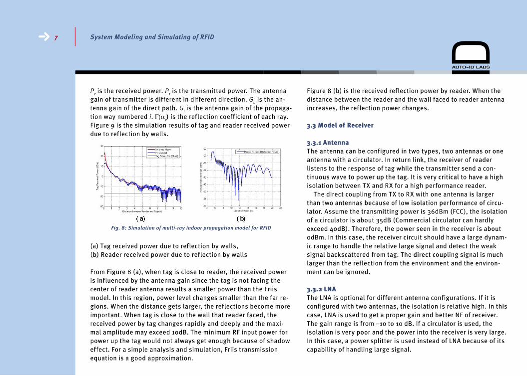
Figure 9 is the simulation results of tag and reader received power due to reflection by walls.
Fig. 8: Simulation of multi-ray indoor propagation model for RFID
(a) Tag received power due to reflection by walls, (b) Reader received power due to reflection by walls
From Figure 8 (a), when tag is close to reader, the received power is influenced by the antenna gain since the tag is not facing the center of reader antenna results a smaller power than the Friis model. In this region, power level changes smaller than the far re-gions. When the distance gets larger, the reflections become more important. When tag is close to the wall that reader faced, the received power by tag changes rapidly and deeply and the maxi-mal amplitude may exceed 10dB. The minimum RF input power for power up the tag would not always get enough because of shadow effect. For a simple analysis and simulation, Friis transmission equation is a good approximation.
Figure 8 (b) is the received reflection power by reader. When the distance between the reader and the wall faced to reader antenna increases, the reflection power changes.
3.3 Model of Receiver
3.3.1 AntennaThe antenna can be configured in two types, two antennas or one antenna with a circulator. In return link, the receiver of reader listens to the response of tag while the transmitter send a con-tinuous wave to power up the tag. It is very critical to have a high isolation between TX and RX for a high performance reader.
The direct coupling from TX to RX with one antenna is larger than two antennas because of low isolation performance of circu-lator. Assume the transmitting power is 36dBm (FCC), the isolation of a circulator is about 35dB (Commercial circulator can hardly exceed 40dB). Therefore, the power seen in the receiver is about 0dBm. In this case, the receiver circuit should have a large dynam-ic range to handle the relative large signal and detect the weak signal backscattered from tag. The direct coupling signal is much larger than the reflection from the environment and the environ-ment can be ignored.
3.3.2 LNAThe LNA is optional for different antenna configurations. If it is configured with two antennas, the isolation is relative high. In this case, LNA is used to get a proper gain and better NF of receiver. The gain range is from –10 to 10 dB. If a circulator is used, the isolation is very poor and the power into the receiver is very large. In this case, a power splitter is used instead of LNA because of its capability of handling large signal.
8 System Modeling and Simulating of RFID
3.3.3 Direct ConversionThe architecture of receiver is direct conversion receiver suitable for multi-protocol operation. The DC offsets are very large due to low isolation between the TX and RX. The receiver will have a multi-stage gain to amplifier the weak signal. Since the DC offset is much larger than the signal, the offset may saturate the ampli-fier if it is not removed. An ac coupling stage is inserted after the mixer filtering out the DC component.
The I/Q mismatch of the receiver is different with the transmit-ter. In receiver, the I/Q mismatch will corrupt the downconverted signal constellation such as QPSK. In RFID system, the modulation used in return link is AM and PSK [8]. It has less influence in the receiver with amplitude modulation.
3.3.4 FilterA high order channel select filter is applied to get a sufficient out of band suppression. The filter type in the receiver is a 5-order Butterworh filter due to it flatness in the passband and suitable for amplitude modulation.
3.3.5 Base-band DSPThe baseband DSP is to decode the signal from ADC. The DSP should combine the signal power of I/Q branch for maximizing the signal power to get the best BER performance. In additional, some filtering must be made to suppress the out of band interference in further. This part is not included in our simulation.
4. Simulation Results
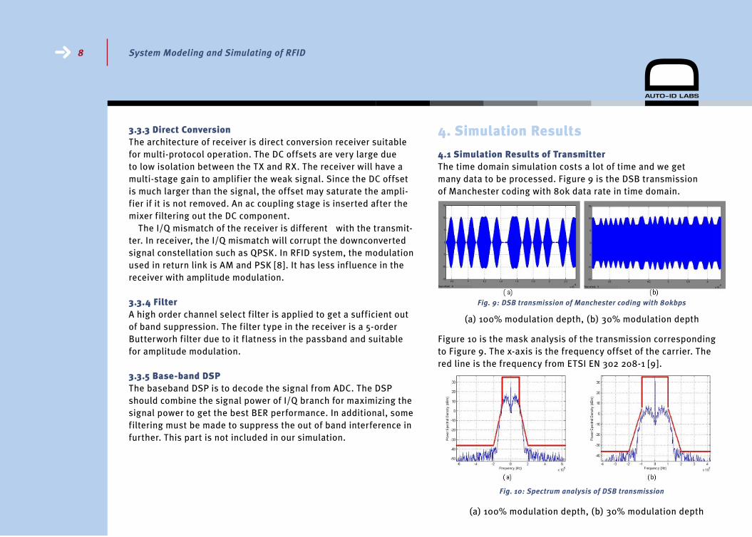
4.1 Simulation Results of TransmitterThe time domain simulation costs a lot of time and we get many data to be processed. Figure 9 is the DSB transmission of Manchester coding with 80k data rate in time domain.
Manchester coding with 80k data rate in time domain.Fig. 9: DSB transmission of Manchester coding with 80kbps
(a) 100% modulation depth, (b) 30% modulation depth
Figure 10 is the mask analysis of the transmission corresponding to Figure 9. The x-axis is the frequency offset of the carrier. The red line is the frequency from ETSI EN 302 208-1 [9].
Fig. 10: Spectrum analysis of DSB transmission
(a) 100% modulation depth, (b) 30% modulation depth
9 System Modeling and Simulating of RFID
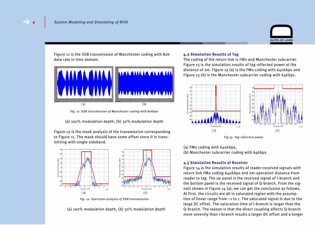
Figure 11 is the SSB transmission of Manchester coding with 80k data rate in time domain.
Fig. 11: SSB transmission of Manchester coding with 80kbps
(a) 100% modulation depth, (b) 30% modulation depth
Figure 12 is the mask analysis of the transmission corresponding to Figure 11. The mask should have some offset since it is trans-mitting with single sideband.
Fig. 12: Spectrum analysis of SSB transmission
(a) 100% modulation depth, (b) 30% modulation depth
4.2 Simulation Results of TagThe coding of the return link is FM0 and Manchester subcarrier. Figure 13 is the simulation results of tag reflected power at the distance of 2m. Figure 13 (a) is the FM0 coding with 640kbps and Figure 13 (b) is the Manchester subcarrier coding with 64kbps.
Fig 13: Tag reflected power
(a) FM0 coding with 640kbps,(b) Manchester subcarrier coding with 64kbps
4.3 Simulation Results of ReceiverFigure 14 is the simulation results of reader-received signals with return link FM0 coding 640kbps and 2m-operation distance from reader to tag. The up panel is the received signal of I-branch and the bottom panel is the received signal of Q-branch. From the sig-nals shown in Figure 14 (a), we can get the conclusion as follows. At first, the circuits are all in saturated region with the assump-tion of linear range from –1 to 1. The saturated signal is due to the large DC offset. The saturation time of I-branch is larger than the Q-branch. The reason is that the direct coupling affects Q-branch more severely than I-branch results a larger DC offset and a longer

10 System Modeling and Simulating of RFID
settling time. The SNR is better in I-branch than in Q-branch. Different results can be obtained by changing the phase delay of the direct coupling and the operation distance from reader to tag, Figure 14 (b). The low frequency noise because of LO phase noise and fluctuation of amplitude can hardly removed. Therefore, the circuit of detector is critical.
Fig. 14: Reader received signals
(a) Example 1, (b) Example 2
(Up panel is I-branch; bottom panel is Q-branch)
5. Conclusion
In this paper, a system model is developed with some simulation results. At first, the simulation model is introduced briefly. Mod-els of DSP, trasmitter and wireless channel, front-end of tag and receiver model are introduced. Finally, some simulation results are presented.
There are some critical problems to be discussed. The raised cosine filter affects the spectrum of the output, and the param-eters should be handled carefully. The SSB transmission is not very ideal from the simulation results since a finite length of data is processed. In receiver of reader, the suppression of DC offset and transient response may drive the follow-up circuits into satu-ration. The bandwidth of channel select filters is also important because it is related to noise floor. Baseband circuits, variable gain stage and detector of receiver are also challenges. The reflec-tion of the objects in environment will mainly affect the operation of tag, and special attention should be paid to diminish the ef-fect of Fresnel zones. All the problems mentioned above should be solved in further study and cost much of efforts to get a best performance.
The system simulation is focused on reader side with a simple wireless channel and a simple reflection model of tag for evaluat-ing the performance of reader. More complicated models should be constructed in frequency domain simulation to determine and optimize the parameters of building blocks of reader and tag.
11 System Modeling and Simulating of RFID
References
[1] MIT Auto-ID Center Publications: http://www.autoidcenter.org
[2] Daniel W. Engels, “The Reader Collision Problem”, MIT-AUTOID-WH-007
[3] EPC Radio-Frequency Identity Protocols Generation 2 Identity Tag (Class 1): Protocol for Communications at 860MHz-960MHz. EPC Global Hardware Action Group (HAG), EPC Identity Tag (Class 1) Generation 2, Last-Call Working Draft Version 1.0.2, 2003-11-24
[4] John G. Proakis, “Digital Communications (Fourth Edition)”, McGraw-Hill Companies, Inc, 2001
[5] Behzad Razavi, “RF Microelectronics”, Prentice Hall, Inc. 1998
[6] David Johns, Ken Martin, “Analog Intergrated Circuit Design”, John Wiley & Sons, Inc, 1997
[7] Udo Karthaus�Martin Fischer�“Fully Integrated Passive UHF RFID Transponder IC With 16.7-uW Minimum RF Input Power” IEEE Journal of Solid-State Circuits, Vol.38, No. 10,
October 2003.
[8] The Palomar system Deliverable D7, Version V2.1,2002
[9] European Standard (Telecommunications series), “Electro-magnetic compatibility and Radio spectrum Matters (ERM); Radio Frequency Identification Equipment operating in the band 865MHz to 868MHz with power levels up to 2W; Part 1: Technical requirements and methods of measurement”, Draft ETSI EN 302 208-1 V1.1.1, 2003-12