Design Equations for Spiral and Scalable Cross Inductors ...
13
Journal of Microwaves, Optoelectronics and Electromagnetic Applications, Vol. 17, No. 3, September 2018 DOI: http://dx.doi.org/10.1590/2179-10742018v17i31215 403 Brazilian Microwave and Optoelectronics Society-SBMO received 20 Jan 2018; for review 25 Jan 2018; accepted 7 Jul 2018 Brazilian Society of Electromagnetism-SBMag © 2012 SBMO/SBMag ISSN 2179-1074 Abstract— This paper presents a set of design equations for spiral and new scalable cross inductors in CMOS 0.35 μm technology, relating electrical parameters of the inductor’s equivalent circuit as functions of its geometric dimensions. The procedure used to derive the design equations is described and involves electromagnetic simulation of inductors with different geometric dimensions, extraction of values for equivalent circuit model elements for each inductor and the use of multivariate regression analysis applied to generalized linear models (GLM) based on Design of Experiments (DoE). A nine element -type equivalent electrical circuit was used for the inductors, where all element values are constants, allowing simulation on SPICE-like software. Results from the models obtained for both spiral and scalable cross inductors presented closely match to the simulated results. Index Terms— Planar inductor, Design of Experiments, EM simulation, Mathematical model. I. INTRODUCTION The design of integrated circuits at the schematic representation level is a fast tool for analog CMOS circuit designers. However, the physical design of components with complex layout, such as planar inductors, is time-consuming and complicated. In most situations, it is not possible to develop simple mathematical models from Maxwell equations that correspond to the geometry of the device and its electrical characteristics, pushing the designer in a cycle of numerous trial and error attempts. Inductors are geometrically much larger than integrated resistors and capacitors used in planar technology, being strongly affected by resistive and capacitive effects that cannot be ignored at high frequencies, requiring complex models and time-consuming simulations. To solve this problem, many researchers have been working to implement simple and efficient electrical equivalent circuit models for planar inductors, to assist RF circuit designers. Some approaches are based on simplified solutions of the Maxwell equations [1] – [2], others use transmission line models [3], and others employ equivalent electric circuits using single-π [4], double- π [5] or T [6] configuration. All these models produce an efficient simulation of the actual behavior of planar inductors. However, they are developed to represent a specific inductor ’s geometry, Design Equations for Spiral and Scalable Cross Inductors on 0.35 μm CMOS Technology José Fontebasso Neto 1 , Luiz Carlos Moreira 1 , Fatima Salete Correra 2 1 Digital and Analog Integrated Circuits Design Laboratory (LPCIAD) Catholic University of Santos, Santos, SP 11015-002 Brazil [email protected], [email protected] 2 Microelectronics Laboratory (LME) Polytechnic School at University of São Paulo, São Paulo, SP 05508-010 Brazil [email protected]
Transcript of Design Equations for Spiral and Scalable Cross Inductors ...
Journal of Microwaves, Optoelectronics and Electromagnetic Applications, Vol. 17, No. 3, September 2018 DOI: http://dx.doi.org/10.1590/2179-10742018v17i31215 403
Brazilian Microwave and Optoelectronics Society-SBMO received 20 Jan 2018; for review 25 Jan 2018; accepted 7 Jul 2018
Brazilian Society of Electromagnetism-SBMag © 2012 SBMO/SBMag ISSN 2179-1074
Abstract— This paper presents a set of design equations for spiral
and new scalable cross inductors in CMOS 0.35 μm technology,
relating electrical parameters of the inductor’s equivalent circuit as
functions of its geometric dimensions. The procedure used to derive
the design equations is described and involves electromagnetic
simulation of inductors with different geometric dimensions,
extraction of values for equivalent circuit model elements for each
inductor and the use of multivariate regression analysis applied to
generalized linear models (GLM) based on Design of Experiments
(DoE). A nine element -type equivalent electrical circuit was used
for the inductors, where all element values are constants, allowing
simulation on SPICE-like software. Results from the models
obtained for both spiral and scalable cross inductors presented
closely match to the simulated results.
Index Terms— Planar inductor, Design of Experiments, EM simulation,
Mathematical model.
I. INTRODUCTION
The design of integrated circuits at the schematic representation level is a fast tool for analog
CMOS circuit designers. However, the physical design of components with complex layout, such as
planar inductors, is time-consuming and complicated. In most situations, it is not possible to develop
simple mathematical models from Maxwell equations that correspond to the geometry of the device
and its electrical characteristics, pushing the designer in a cycle of numerous trial and error attempts.
Inductors are geometrically much larger than integrated resistors and capacitors used in planar
technology, being strongly affected by resistive and capacitive effects that cannot be ignored at high
frequencies, requiring complex models and time-consuming simulations.
To solve this problem, many researchers have been working to implement simple and efficient
electrical equivalent circuit models for planar inductors, to assist RF circuit designers. Some
approaches are based on simplified solutions of the Maxwell equations [1] – [2], others use
transmission line models [3], and others employ equivalent electric circuits using single-π [4], double-
π [5] or T [6] configuration. All these models produce an efficient simulation of the actual behavior of
planar inductors. However, they are developed to represent a specific inductor’s geometry,
Design Equations for Spiral and Scalable
Cross Inductors on 0.35 μm CMOS
Technology José Fontebasso Neto
1, Luiz Carlos Moreira
1, Fatima Salete Correra
2
1Digital and Analog Integrated Circuits Design Laboratory (LPCIAD)
Catholic University of Santos, Santos, SP 11015-002 Brazil [email protected], [email protected]
2Microelectronics Laboratory (LME)
Polytechnic School at University of São Paulo, São Paulo, SP 05508-010 Brazil
Journal of Microwaves, Optoelectronics and Electromagnetic Applications, Vol. 17, No. 3, September 2018 DOI: http://dx.doi.org/10.1590/2179-10742018v17i31215 404
Brazilian Microwave and Optoelectronics Society-SBMO received 20 Jan 2018; for review 25 Jan 2018; accepted 7 Jul 2018
Brazilian Society of Electromagnetism-SBMag © 2012 SBMO/SBMag ISSN 2179-1074
manufactured using a given semiconductor technology, or the procedure used to extract the value of
the model elements is complicated. Alternatively, the electrical characteristics of the inductor are
obtained considering the individual contribution of all its segments, requiring a considerable number
of calculations to model the inductor behavior from its geometry.
As a contribution, this paper presents a procedure to develop design equations to express the value
of each element of the inductor equivalent circuit model as a function of its geometric dimensions.
The equations are generated by multivariate regression analysis applied to generalized linear models
(GLM) [7] based on Design of Experiments (DoE) [8]. The proposed procedure was applied to
develop –type equivalent circuit models for spiral and scalable cross inductors on CMOS 0.35 µm
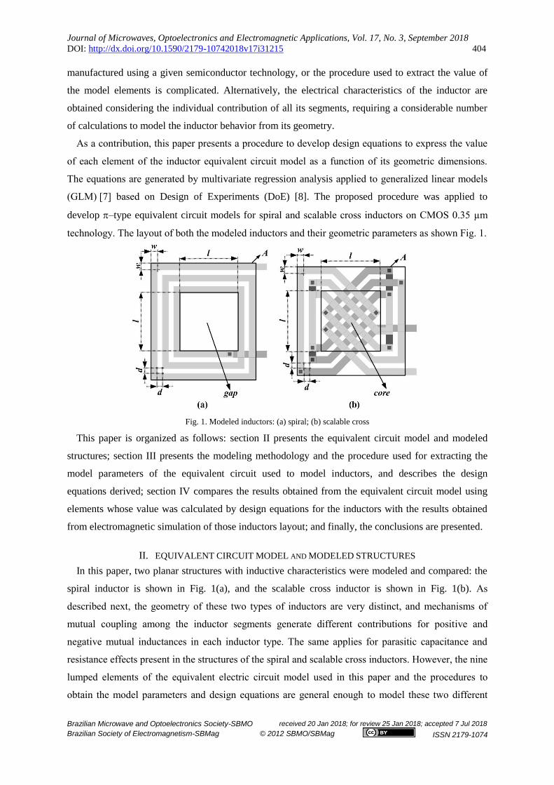
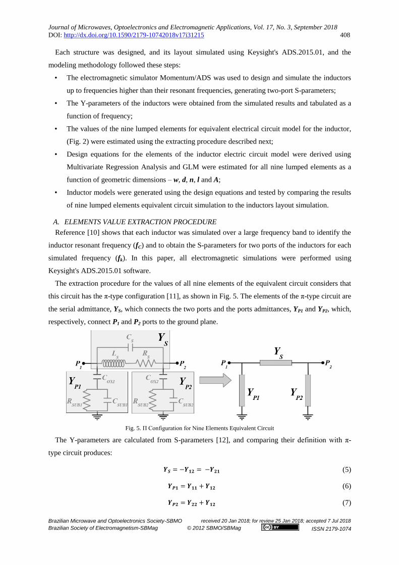
technology. The layout of both the modeled inductors and their geometric parameters as shown Fig. 1.
Fig. 1. Modeled inductors: (a) spiral; (b) scalable cross
This paper is organized as follows: section II presents the equivalent circuit model and modeled
structures; section III presents the modeling methodology and the procedure used for extracting the
model parameters of the equivalent circuit used to model inductors, and describes the design
equations derived; section IV compares the results obtained from the equivalent circuit model using
elements whose value was calculated by design equations for the inductors with the results obtained
from electromagnetic simulation of those inductors layout; and finally, the conclusions are presented.
II. EQUIVALENT CIRCUIT MODEL AND MODELED STRUCTURES
In this paper, two planar structures with inductive characteristics were modeled and compared: the
spiral inductor is shown in Fig. 1(a), and the scalable cross inductor is shown in Fig. 1(b). As
described next, the geometry of these two types of inductors are very distinct, and mechanisms of
mutual coupling among the inductor segments generate different contributions for positive and
negative mutual inductances in each inductor type. The same applies for parasitic capacitance and
resistance effects present in the structures of the spiral and scalable cross inductors. However, the nine
lumped elements of the equivalent electric circuit model used in this paper and the procedures to
obtain the model parameters and design equations are general enough to model these two different
Journal of Microwaves, Optoelectronics and Electromagnetic Applications, Vol. 17, No. 3, September 2018 DOI: http://dx.doi.org/10.1590/2179-10742018v17i31215 405
Brazilian Microwave and Optoelectronics Society-SBMO received 20 Jan 2018; for review 25 Jan 2018; accepted 7 Jul 2018
Brazilian Society of Electromagnetism-SBMag © 2012 SBMO/SBMag ISSN 2179-1074
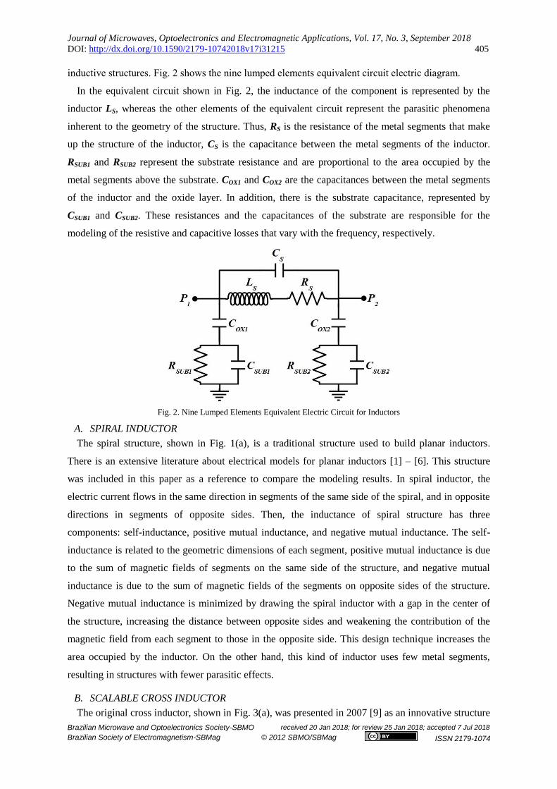
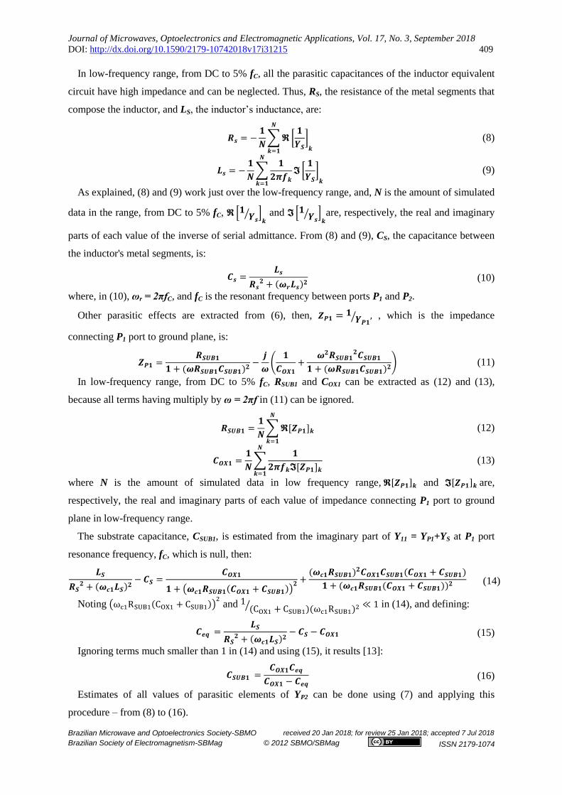
inductive structures. Fig. 2 shows the nine lumped elements equivalent circuit electric diagram.
In the equivalent circuit shown in Fig. 2, the inductance of the component is represented by the
inductor LS, whereas the other elements of the equivalent circuit represent the parasitic phenomena
inherent to the geometry of the structure. Thus, RS is the resistance of the metal segments that make
up the structure of the inductor, CS is the capacitance between the metal segments of the inductor.
RSUB1 and RSUB2 represent the substrate resistance and are proportional to the area occupied by the
metal segments above the substrate. COX1 and COX2 are the capacitances between the metal segments
of the inductor and the oxide layer. In addition, there is the substrate capacitance, represented by
CSUB1 and CSUB2. These resistances and the capacitances of the substrate are responsible for the
modeling of the resistive and capacitive losses that vary with the frequency, respectively.
Fig. 2. Nine Lumped Elements Equivalent Electric Circuit for Inductors
A. SPIRAL INDUCTOR
The spiral structure, shown in Fig. 1(a), is a traditional structure used to build planar inductors.
There is an extensive literature about electrical models for planar inductors [1] – [6]. This structure
was included in this paper as a reference to compare the modeling results. In spiral inductor, the
electric current flows in the same direction in segments of the same side of the spiral, and in opposite
directions in segments of opposite sides. Then, the inductance of spiral structure has three
components: self-inductance, positive mutual inductance, and negative mutual inductance. The self-
inductance is related to the geometric dimensions of each segment, positive mutual inductance is due
to the sum of magnetic fields of segments on the same side of the structure, and negative mutual
inductance is due to the sum of magnetic fields of the segments on opposite sides of the structure.
Negative mutual inductance is minimized by drawing the spiral inductor with a gap in the center of
the structure, increasing the distance between opposite sides and weakening the contribution of the
magnetic field from each segment to those in the opposite side. This design technique increases the
area occupied by the inductor. On the other hand, this kind of inductor uses few metal segments,
resulting in structures with fewer parasitic effects.
B. SCALABLE CROSS INDUCTOR
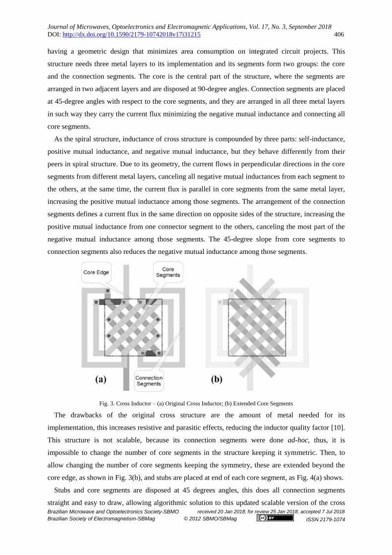
The original cross inductor, shown in Fig. 3(a), was presented in 2007 [9] as an innovative structure
Journal of Microwaves, Optoelectronics and Electromagnetic Applications, Vol. 17, No. 3, September 2018 DOI: http://dx.doi.org/10.1590/2179-10742018v17i31215 406
Brazilian Microwave and Optoelectronics Society-SBMO received 20 Jan 2018; for review 25 Jan 2018; accepted 7 Jul 2018
Brazilian Society of Electromagnetism-SBMag © 2012 SBMO/SBMag ISSN 2179-1074
having a geometric design that minimizes area consumption on integrated circuit projects. This
structure needs three metal layers to its implementation and its segments form two groups: the core
and the connection segments. The core is the central part of the structure, where the segments are
arranged in two adjacent layers and are disposed at 90-degree angles. Connection segments are placed
at 45-degree angles with respect to the core segments, and they are arranged in all three metal layers
in such way they carry the current flux minimizing the negative mutual inductance and connecting all
core segments.
As the spiral structure, inductance of cross structure is compounded by three parts: self-inductance,
positive mutual inductance, and negative mutual inductance, but they behave differently from their
peers in spiral structure. Due to its geometry, the current flows in perpendicular directions in the core
segments from different metal layers, canceling all negative mutual inductances from each segment to
the others, at the same time, the current flux is parallel in core segments from the same metal layer,
increasing the positive mutual inductance among those segments. The arrangement of the connection
segments defines a current flux in the same direction on opposite sides of the structure, increasing the
positive mutual inductance from one connector segment to the others, canceling the most part of the
negative mutual inductance among those segments. The 45-degree slope from core segments to
connection segments also reduces the negative mutual inductance among those segments.
Fig. 3. Cross Inductor – (a) Original Cross Inductor; (b) Extended Core Segments
The drawbacks of the original cross structure are the amount of metal needed for its
implementation, this increases resistive and parasitic effects, reducing the inductor quality factor [10].
This structure is not scalable, because its connection segments were done ad-hoc, thus, it is
impossible to change the number of core segments in the structure keeping it symmetric. Then, to
allow changing the number of core segments keeping the symmetry, these are extended beyond the
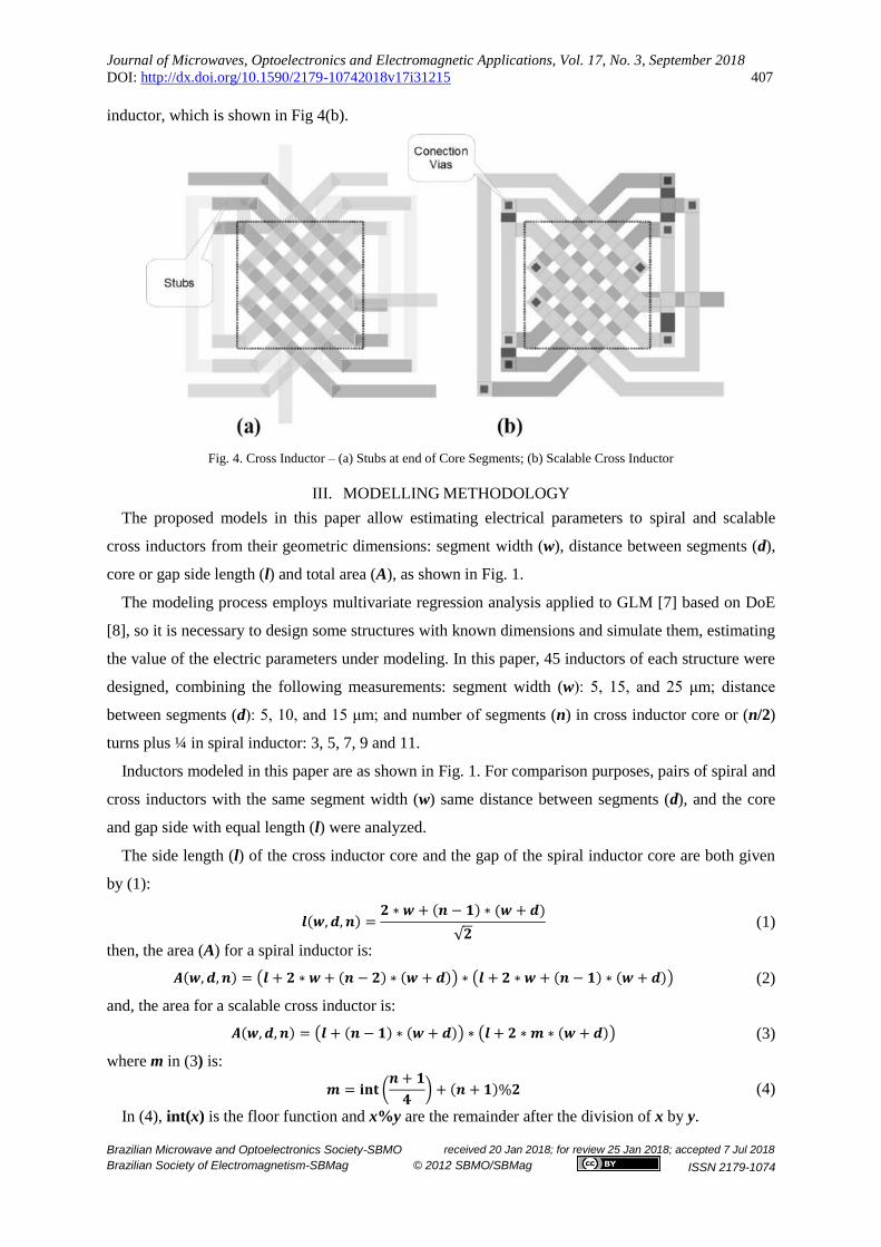
core edge, as shown in Fig. 3(b), and stubs are placed at end of each core segment, as Fig. 4(a) shows.
Stubs and core segments are disposed at 45 degrees angles, this does all connection segments
straight and easy to draw, allowing algorithmic solution to this updated scalable version of the cross
Journal of Microwaves, Optoelectronics and Electromagnetic Applications, Vol. 17, No. 3, September 2018 DOI: http://dx.doi.org/10.1590/2179-10742018v17i31215 407
Brazilian Microwave and Optoelectronics Society-SBMO received 20 Jan 2018; for review 25 Jan 2018; accepted 7 Jul 2018
Brazilian Society of Electromagnetism-SBMag © 2012 SBMO/SBMag ISSN 2179-1074
inductor, which is shown in Fig 4(b).
Fig. 4. Cross Inductor – (a) Stubs at end of Core Segments; (b) Scalable Cross Inductor
III. MODELLING METHODOLOGY
The proposed models in this paper allow estimating electrical parameters to spiral and scalable
cross inductors from their geometric dimensions: segment width (w), distance between segments (d),
core or gap side length (l) and total area (A), as shown in Fig. 1.
The modeling process employs multivariate regression analysis applied to GLM [7] based on DoE
[8], so it is necessary to design some structures with known dimensions and simulate them, estimating
the value of the electric parameters under modeling. In this paper, 45 inductors of each structure were
designed, combining the following measurements: segment width (w): 5, 15, and 25 μm; distance
between segments (d): 5, 10, and 15 μm; and number of segments (n) in cross inductor core or (n/2)
turns plus ¼ in spiral inductor: 3, 5, 7, 9 and 11.
Inductors modeled in this paper are as shown in Fig. 1. For comparison purposes, pairs of spiral and
cross inductors with the same segment width (w) same distance between segments (d), and the core
and gap side with equal length (l) were analyzed.
The side length (l) of the cross inductor core and the gap of the spiral inductor core are both given
by (1):
(1)
then, the area (A) for a spiral inductor is:
(2)
and, the area for a scalable cross inductor is:
(3)
where m in (3) is:
(4)
In (4), int(x) is the floor function and x%y are the remainder after the division of x by y.
Journal of Microwaves, Optoelectronics and Electromagnetic Applications, Vol. 17, No. 3, September 2018 DOI: http://dx.doi.org/10.1590/2179-10742018v17i31215 408
Brazilian Microwave and Optoelectronics Society-SBMO received 20 Jan 2018; for review 25 Jan 2018; accepted 7 Jul 2018
Brazilian Society of Electromagnetism-SBMag © 2012 SBMO/SBMag ISSN 2179-1074
Each structure was designed, and its layout simulated using Keysight's ADS.2015.01, and the
modeling methodology followed these steps:
• The electromagnetic simulator Momentum/ADS was used to design and simulate the inductors
up to frequencies higher than their resonant frequencies, generating two-port S-parameters;
• The Y-parameters of the inductors were obtained from the simulated results and tabulated as a
function of frequency;
• The values of the nine lumped elements for equivalent electrical circuit model for the inductor,
(Fig. 2) were estimated using the extracting procedure described next;
• Design equations for the elements of the inductor electric circuit model were derived using
Multivariate Regression Analysis and GLM were estimated for all nine lumped elements as a
function of geometric dimensions – w, d, n, l and A;
• Inductor models were generated using the design equations and tested by comparing the results
of nine lumped elements equivalent circuit simulation to the inductors layout simulation.
A. ELEMENTS VALUE EXTRACTION PROCEDURE
Reference [10] shows that each inductor was simulated over a large frequency band to identify the
inductor resonant frequency (fC) and to obtain the S-parameters for two ports of the inductors for each
simulated frequency (fk). In this paper, all electromagnetic simulations were performed using
Keysight's ADS.2015.01 software.
The extraction procedure for the values of all nine elements of the equivalent circuit considers that
this circuit has the π-type configuration [11], as shown in Fig. 5. The elements of the π-type circuit are
the serial admittance, YS, which connects the two ports and the ports admittances, YP1 and YP2, which,
respectively, connect P1 and P2 ports to the ground plane.
Fig. 5. Π Configuration for Nine Elements Equivalent Circuit
The Y-parameters are calculated from S-parameters [12], and comparing their definition with π-
type circuit produces:
(5)
(6)
(7)
Journal of Microwaves, Optoelectronics and Electromagnetic Applications, Vol. 17, No. 3, September 2018 DOI: http://dx.doi.org/10.1590/2179-10742018v17i31215 409
Brazilian Microwave and Optoelectronics Society-SBMO received 20 Jan 2018; for review 25 Jan 2018; accepted 7 Jul 2018
Brazilian Society of Electromagnetism-SBMag © 2012 SBMO/SBMag ISSN 2179-1074
In low-frequency range, from DC to 5% fC, all the parasitic capacitances of the inductor equivalent
circuit have high impedance and can be neglected. Thus, RS, the resistance of the metal segments that
compose the inductor, and LS, the inductor’s inductance, are:
(8)
(9)
As explained, (8) and (9) work just over the low-frequency range, and, N is the amount of simulated
data in the range, from DC to 5% fC,
and
are, respectively, the real and imaginary
parts of each value of the inverse of serial admittance. From (8) and (9), CS, the capacitance between
the inductor's metal segments, is:
(10)
where, in (10), ωr = 2πfC, and fC is the resonant frequency between ports P1 and P2.
Other parasitic effects are extracted from (6), then, , which is the impedance
connecting P1 port to ground plane, is:
(11)
In low-frequency range, from DC to 5% fC, RSUB1 and COX1 can be extracted as (12) and (13),
because all terms having multiply by ω = 2πf in (11) can be ignored.
(12)
(13)
where N is the amount of simulated data in low frequency range, and are,
respectively, the real and imaginary parts of each value of impedance connecting P1 port to ground
plane in low-frequency range.
The substrate capacitance, CSUB1, is estimated from the imaginary part of Y11 = YP1+YS at P1 port
resonance frequency, fC, which is null, then:
(14)
Noting and
in (14), and defining:
(15)
Ignoring terms much smaller than 1 in (14) and using (15), it results [13]:
(16)
Estimates of all values of parasitic elements of YP2 can be done using (7) and applying this
procedure – from (8) to (16).
Journal of Microwaves, Optoelectronics and Electromagnetic Applications, Vol. 17, No. 3, September 2018 DOI: http://dx.doi.org/10.1590/2179-10742018v17i31215 410
Brazilian Microwave and Optoelectronics Society-SBMO received 20 Jan 2018; for review 25 Jan 2018; accepted 7 Jul 2018
Brazilian Society of Electromagnetism-SBMag © 2012 SBMO/SBMag ISSN 2179-1074
B. DESIGN EQUATIONS
Parameter extraction procedure estimates values for electrical parameters only to designed
inductors but it does not help the design of inductors with different geometrical dimensions. Thus, a
set of equations relating the inductor geometric dimensions to the electrical parameters of its
equivalent circuit model were derived, allowing to design any similar inductor in the range of
dimensions used in the element values extraction procedure.
The procedure using GLM based on DoE and Multivariate Regression Analysis is an excellent tool
to relate the geometric dimensions to the electrical parameters in this case because it can relate any
kind of free variables to the output ones. In this paper, the geometric dimensions of inductors – w, d,
n, l and A – are free variables and the electrical parameters of nine elements equivalent circuit for
inductors – LS, RS, CS, COX1, RSUB1, CSUB1, COX2, RSUB2 and CSUB2 – are output variables.
In few words, DoE [8] is a method to estimate how a group of free variables affects an output
variable by a limited number of attempts to discover how this happens. This is possible by a choice of
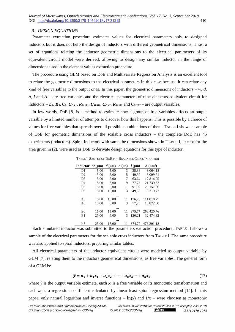
values for free variables that spreads over all possible combinations of them. TABLE I shows a sample
of DoE for geometric dimensions of the scalable cross inductors – the complete DoE has 45
experiments (inductors). Spiral inductors with same the dimensions shown in TABLE I, except for the
area given in (2), were used as DoE to derivate design equations for this type of inductor.
TABLE I: SAMPLE OF DOE FOR SCALABLE CROSS INDUCTOR
Inductor w (μm) d (μm) n (un) l (μm) A (μm2)
I01 5,00 5,00 3 35,36 3.064,18
I02 5,00 5,00 5 49,50 8.009,71
I03 5,00 5,00 7 63,64 12.814,05
I04 5,00 5,00 9 77,78 21.739,52
I05 5,00 5,00 11 91,92 29.157,86
I06 5,00 10,00 3 49,50 6.319,77
...
I15 5,00 15,00 11 176,78 111.818,75
I16 15,00 5,00 3 77,78 13.872,60
...
I30 15,00 15,00 11 275,77 262.420,76
I31 25,00 5,00 3 120,21 32.474,92
...
I45 25,00 15,00 11 374,77 476.301,18
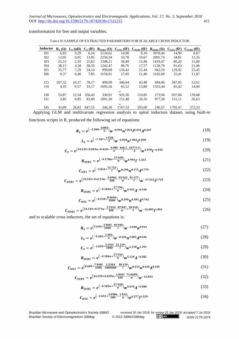
Each simulated inductor was submitted to the parameters extraction procedure, TABLE II shows a
sample of the electrical parameters for the scalable cross inductors from TABLE I. The same procedure
was also applied to spiral inductors, preparing similar tables.
All electrical parameters of the inductor equivalent circuit were modeled as output variable by
GLM [7], relating them to the inductors geometrical dimensions, as free variables. The general form
of a GLM is:
(17)
where ŷ is the output variable estimate, each xi is a free variable or its monotonic transformation and
each αi is a regression coefficient calculated by linear least spiral regression method [14]. In this
paper, only natural logarithm and inverse functions – ln(x) and 1/x – were choosen as monotonic
Journal of Microwaves, Optoelectronics and Electromagnetic Applications, Vol. 17, No. 3, September 2018 DOI: http://dx.doi.org/10.1590/2179-10742018v17i31215 411
Brazilian Microwave and Optoelectronics Society-SBMO received 20 Jan 2018; for review 25 Jan 2018; accepted 7 Jul 2018
Brazilian Society of Electromagnetism-SBMag © 2012 SBMO/SBMag ISSN 2179-1074
transformation for free and output variables.
TABLE II: SAMPLE OF EXTRACTED PARAMETERS FOR SCALABLE CROSS INDUCTOR
Inductor RS (Ω) LS (nH) CS (fF) RSUB1 (Ω) COX1 (fF) CSUB1 (fF) RSUB2 (Ω) COX2 (fF) CSUB2 (fF)
I01 6,83 0,29 6,24 3124,62 14,90 8,10 3078,44 14,90 8,67
I02 13,95 0,91 13,85 2250,34 33,78 10,67 2091,74 34,81 12,35
I03 25,23 2,10 25,63 1508,21 58,49 13,46 1419,47 60,20 15,80
I04 38,13 4,18 38,35 1242,47 88,76 17,57 1128,79 91,63 21,06
I05 55,77 7,29 54,14 999,69 126,42 21,44 942,59 129,92 25,45
I06 9,37 0,48 7,85 3159,91 27,85 11,40 3182,68 25,41 11,87
... I15 107,52 16,37 78,17 499,09 346,64 43,48 494,96 347,95 52,61
I16 4,35 0,57 33,17 1695,56 65,52 13,80 1555,44 65,42 14,00
... I30 53,87 22,54 356,43 330,91 925,56 110,85 273,94 937,06 139,68
I31 3,85 0,85 83,00 1091,50 151,48 26,16 977,58 151,11 26,63
... I45 43,09 28,82 847,55 246,30 1767,53 293,00 240,57 1795,47 372,33
Applying GLM and multivariate regression analysis to spiral inductors dataset, using built-in
functions scripts in R, produced the following set of equations:
(18)
(19)
(20)
(21)
(22)
(23)
(24)
(25)
(26)
and to scalable cross inductors, the set of equations is:
(27)
(28)
(29)
(30)
(31)
(32)
(33)
(34)
Journal of Microwaves, Optoelectronics and Electromagnetic Applications, Vol. 17, No. 3, September 2018 DOI: http://dx.doi.org/10.1590/2179-10742018v17i31215 412
Brazilian Microwave and Optoelectronics Society-SBMO received 20 Jan 2018; for review 25 Jan 2018; accepted 7 Jul 2018
Brazilian Society of Electromagnetism-SBMag © 2012 SBMO/SBMag ISSN 2179-1074
(35)
There are many combinations of free variables and their monotonic transformations to model the
output variable. Then, multivariate regression analysis, controlled by t-test and analysis of variance
for the free variables coefficients, helps to choose a combination of free variables which has statistical
significance to estimate the output variable [7] [8]. This explains why some free variables, like
distance between segments, d, appear only in few equations, whereas others, like segment width, w,
appear in all equations.
Equations (18) to (35) are design equations for spiral and scalable cross inductors in CMOS
0.35 µm technology. However, the procedures used to obtain these equations can be applied to
generate design equations for different inductive structures fabricated in other technologies
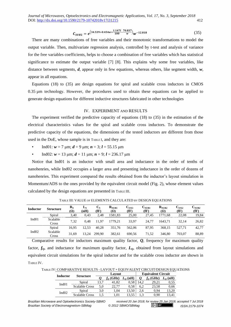
IV. EXPERIMENT AND RESULTS
The experiment verified the predictive capacity of equations (18) to (35) in the estimation of the
electrical characteristics values for the spiral and scalable cross inductors. To demonstrate the
predictive capacity of the equations, the dimensions of the tested inductors are different from those
used in the DoE, whose sample is in TABLE I, and they are:
• Ind01: w = 7 μm; d = 9 μm; n = 3; l = 55.15 μm
• Ind02: w = 13 μm; d = 11 μm; n = 9; l = 236.17 μm
Notice that Ind01 is an inductor with small area and inductance in the order of tenths of
nanohenries, while Ind02 occupies a larger area and presenting inductance in the order of dozens of
nanohenries. This experiment compared the results obtained from the inductor’s layout simulation in
Momentum/ADS to the ones provided by the equivalent circuit model (Fig. 2), whose element values
calculated by the design equations are presented in TABLE III.
TABLE III: VALUE OF ELEMENTS CALCULATED BY DESIGN EQUATIONS
Inductor Structure RS
(Ω)
LS
(nH)
CS
(fF)
RSUB1
(Ω)
COX1
(fF)
CSUB1
(fF)
RSUB2
(Ω)
COX2
(fF)
CSUB2
(fF)
Ind01
Spiral 3,40 0,43 2,48 1581,83 25,00 27,45 1771,68 22,08 19,84
Scalable
Cross 7,32 0,48 11,97 1779,21 33,97 24,77 1643,71 32,14 26,82
Ind02
Spiral 16,95 12,53 40,28 351,76 562,06 87,95 368,15 527,71 42,77
Scalable
Cross 31,69 13,24 299,90 382,61 690,56 71,52 346,80 703,07 88,89
Comparative results for inductors maximum quality factor, Q, frequency for maximum quality
factor, fQ, and inductance for maximum quality factor, LQ, obtained from layout simulations and
equivalent circuit simulations for the spiral inductor and for the scalable cross inductor are shown in
TABLE IV.
TABLE IV: COMPARATIVE RESULTS - LAYOUT × EQUIVALENT CIRCUIT/DESIGN EQUATIONS
Inductor Structure Layout Equivalent Circuit
Q fQ (GHz) LQ (nH) Q fQ (GHz) LQ (nH)
Ind01 Spiral 13,7 41,82 0,58 14,2 29,21 0,55
Scalable Cross 5,0 22,77 0,58 6,2 23,58 0,66
Ind02 Spiral 3,0 1,04 13,50 2,6 0,94 13,20
Scalable Cross 1,5 1,01 13,55 1,3 0,90 13,41
Journal of Microwaves, Optoelectronics and Electromagnetic Applications, Vol. 17, No. 3, September 2018 DOI: http://dx.doi.org/10.1590/2179-10742018v17i31215 413
Brazilian Microwave and Optoelectronics Society-SBMO received 20 Jan 2018; for review 25 Jan 2018; accepted 7 Jul 2018
Brazilian Society of Electromagnetism-SBMag © 2012 SBMO/SBMag ISSN 2179-1074
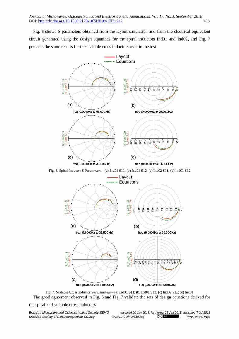
Fig. 6 shows S parameters obtained from the layout simulation and from the electrical equivalent
circuit generated using the design equations for the spiral inductors Ind01 and Ind02, and Fig. 7
presents the same results for the scalable cross inductors used in the test.
The good agreement observed in Fig. 6 and Fig. 7 validate the sets of design equations derived for
the spiral and scalable cross inductors.
Fig. 6. Spiral Inductor S-Parameters – (a) Ind01 S11; (b) Ind01 S12; (c) Ind02 S11; (d) Ind01 S12
Fig. 7. Scalable Cross Inductor S-Parameters – (a) Ind01 S11; (b) Ind01 S12; (c) Ind02 S11; (d) Ind01
S12
Journal of Microwaves, Optoelectronics and Electromagnetic Applications, Vol. 17, No. 3, September 2018 DOI: http://dx.doi.org/10.1590/2179-10742018v17i31215 414
Brazilian Microwave and Optoelectronics Society-SBMO received 20 Jan 2018; for review 25 Jan 2018; accepted 7 Jul 2018
Brazilian Society of Electromagnetism-SBMag © 2012 SBMO/SBMag ISSN 2179-1074
Paired t-tests at 95% confidence level [7] [8] applied at TABLE IV data, comparing each layout
column with each equivalent circuit column for inductor and structure, show a very good agreement
level between results of layout simulations and equivalent circuit simulations indicating that design
equations (18) – (35) produce correct predictions for the values of all nine equivalent circuit elements,
in spite of difference in maximum quality factor frequency, fQ, simulated and calculated for small
spiral inductor, Ind01. This difference happens because the parasitic effects on small spiral inductors
have an order of magnitude similar to the inductive effects and the electromagnetic simulation
reproduce them, while the equivalent circuit does not.
Other results that compare the characteristics of spiral and scalable cross inductors are extracted by
a simple nonlinear regression procedure [7] [8] using TABLE I and electromagnetic simulation data.
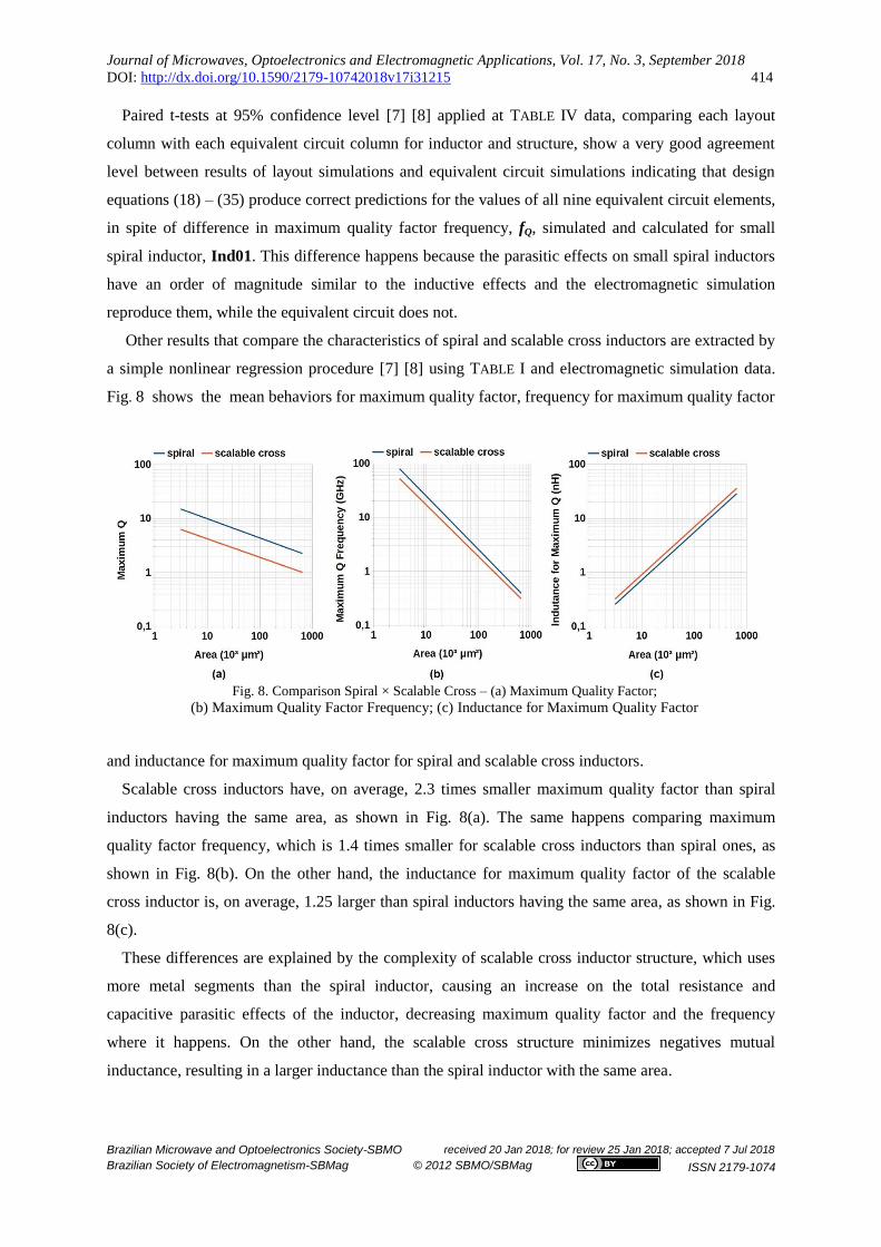
Fig. 8 shows the mean behaviors for maximum quality factor, frequency for maximum quality factor
and inductance for maximum quality factor for spiral and scalable cross inductors.
Scalable cross inductors have, on average, 2.3 times smaller maximum quality factor than spiral
inductors having the same area, as shown in Fig. 8(a). The same happens comparing maximum
quality factor frequency, which is 1.4 times smaller for scalable cross inductors than spiral ones, as
shown in Fig. 8(b). On the other hand, the inductance for maximum quality factor of the scalable
cross inductor is, on average, 1.25 larger than spiral inductors having the same area, as shown in Fig.
8(c).
These differences are explained by the complexity of scalable cross inductor structure, which uses
more metal segments than the spiral inductor, causing an increase on the total resistance and
capacitive parasitic effects of the inductor, decreasing maximum quality factor and the frequency
where it happens. On the other hand, the scalable cross structure minimizes negatives mutual
inductance, resulting in a larger inductance than the spiral inductor with the same area.
Fig. 8. Comparison Spiral × Scalable Cross – (a) Maximum Quality Factor; (b) Maximum Quality Factor Frequency; (c) Inductance for Maximum Quality Factor
Journal of Microwaves, Optoelectronics and Electromagnetic Applications, Vol. 17, No. 3, September 2018 DOI: http://dx.doi.org/10.1590/2179-10742018v17i31215 415
Brazilian Microwave and Optoelectronics Society-SBMO received 20 Jan 2018; for review 25 Jan 2018; accepted 7 Jul 2018
Brazilian Society of Electromagnetism-SBMag © 2012 SBMO/SBMag ISSN 2179-1074
V. CONCLUSIONS
The nine elements equivalent electrical circuit model calculated by design equations to represent
spiral and scalable cross inductors in CMOS 0.35 µm technology, produced results in good agreement
with electromagnetic simulations of the inductor’s layout.
The design equations derived for spiral and scalable cross inductors have good scalability, allowing
estimate inductors features for areas ranging from 3,000 to 650,000 μm2.
Scalable cross inductors were compared to spiral inductors, showing larger inductance per area, and
a smaller quality factor than typical spiral inductor, and they are an interesting choice for applications
where a large quality factor is not mandatory or having restrictions in the area.
The procedures used to develop the electrical equivalent circuit models and design equations for the
scalable cross and spiral inductors were validated and can be applied to other inductive structures and
manufacturing technologies.
REFERENCES
[1] F. W. Grover, Inductance Calculations, New York: D. Van Nostrand, 1946.
[2] R. Thüringer, “Characterization of integrated Lumped inductors and Transformers,” Technischen Universität Wien,
Wien, 2002.
[3] J. Brinkhoff, K. S. S. Koh, K. Kang e F. Lin, “Scalable Transmission Line and Inductor Models for CMOS Millimeter-
Wave Design,” EEE Transactions on Microwave Theory and Techniques, vol. 56, nº 12, pp. 2954-2962, 2008.
[4] J. Gil e H. Shin, “Simple wide-band on-chip inductor model for silicon-based RFICs,” em International Conference on
Simulation of Semiconductor Processes and Devices, SISPAD 2003, Boston, Massachusetts, USA, 2003.
[5] Y. Cao e e. alli, “Frequency-independent equivalent-circuit model for on-chip spiral inductors,” IEEE Journal of Solid-
State Circuits, vol. 38, nº 3, pp. 419-426, Mar 2003.
[6] J. W. Jeong e e. alli, “Modeling of T-model equivalent circuit for spiral inductors in 90 nm CMOS technology,” em
Proceedings of the 2015 International Conference on Microelectronic Test Structures, Tempe, Arizona, USA, 2015.
[7] D. G. Kleinbaum, L. L. Kupper, K. E. Muller e A. Nizam, Applied Regression Analysis and Other Multivariable
Methods, 3 ed., Pacific Grove, California, USA: Duxbury Press, 1997, p. 798.
[8] R. L. Mason, R. F. Gunst e J. L. Hess, Statistical Design and Analysis of Experiments, with Applications to
Engineering and Science, New York: Jonh Wiley & Sons, 1989, p. 720.
[9] L. Moreira, W. Van Noije, A. Farfan-Pelaez e A. dos Anjos, “Small area cross type integrated inductor in CMOS
Technology,” em IMOC 2007 - Microwave and Optoelectronics Conference, 2007.
[10] E. Rios, S. Garcia, L. Moreira, R. Torres e W. Van Noije, “Analysis of the effects of coupling through substrate and the
calculus of the Q factor,” em 2013 IEEE Fourth Latin American Symposium on Circuits and Systems (LASCAS), 2013.
[11] H. H. Chen, H. W. Zhang, S. J. Chung, J. T. Kuo e T. C. Wu, “Accurate Systematic Model-Parameter Extraction for
On-Chip Spiral Inductors,” IEEE Transactions on Electron Devices, vol. 55, nº 11, pp. 3267-3273, Nov 2008.
[12] D. A. Frickey, “Conversions between S, Z, Y, H, ABCD, and T parameters which are valid for complex source and
load impedances,” IEEE Transactions on Microwave Theory and Techniques, vol. 42, nº 2, pp. 205-211, Feb 1994.
[13] N.-J. Oh e S.-G. Lee, “A Simple Model Parameter Extraction Methodology for an On-Chip Spiral Inductor,” ETRI
Journal, vol. 28, p. 115–118, 2006.
[14] E. Pettenpaul e e. alli, “CAD models of lumped elements on GaAs up to 18 GHz,” IEEE Transactions on Microwave
Theory and Techniques, vol. 36, nº 2, pp. 294-304, 1988.
[15] A. M. Niknejad, “Analysis, Simulation, and Applications of Passive Devices on Conductive Substrates,” University of
California, Berkeley, 2000.