Atlas Simulation of a Wide Bandgap Ga O MOSFET 2 3 · eral times larger value of Baliga’s figure...
3
October, November, December 2013 Page 7 The Simulation Standard Atlas Simulation of a Wide Bandgap Ga 2 O 3 MOSFET Figure 1. Device structure and doping profile. 4H-SiC GaN β-Ga 2 O 3 Bandgap Eg [eV] 3.3 (3.23) 3.4 (3.43) 4.8 Electron mobility μ [cm 2 /Vs] 1000 (460) 1200 (400) 300 Breakdown field Eb [MV/cm] 2.5 3.3 8 Relative dielectric constant ε 9.7 (9.7) 9.0 (8.9) 10 BFOM a ε×μ×Eb 3 340 870 3444 Intrinsic carrier concentration Ni [1/cm 3 ] (1.73E-8) (1.06E-10) (1.79E-22) Table 1. “Material properties of wide bandgap semiconductors. These figures are taken from reference [2] except for the figures in parentheses which are from Atlas device simulator. Introduction Single-crystal gallium oxide (Ga 2 O 3 ) has attracted increas- ing attention as a promising material for power device applications. It possesses excellent material properties and has the potential for mass productivity of low-cost and high-quality bulk crystals by using methods such as the edge-defined film-fed growth (EFG) method [1]. Table 1 shows Ga 2 O 3 material properties compared with major wide bandgap semiconductors, 4H-SiC and GaN. It is remarkable that Ga 2 O 3 has a wider bandgap and sev- eral times larger value of Baliga’s figure of merit (BFOM) than those of 4H-SiC and GaN. This indicates that Ga 2 O 3 has an advantage in minimizing conduction losses of power FETs, and it can be expected to exceed 4H-SiC and GaN performances when used for high-power and high- voltage applications. On the other hand, from a numerical simulation point of view, the wider the bandgap becomes the more dif- ficult it is to get stable convergence, because the intrinsic carrier concentration becomes too low to estimate exact leakage current in the carrier continuity equations. The objective of this article is to show the Atlas appli- cability for this new wide bandgap oxide semiconduc- tor material Ga 2 O 3 and to reveal what kinds of physical models and settings (traps and charges, etc.) are needed in order to reproduce experimental I-V data. Device Structure and Material Parameters The experimental data used in this benchmark were select- ed from a recently reported paper on the first demonstra- tion of Ga 2 O 3 MOSFET [3]. The simulated device structure cross section and doping profile are shown in Figure 1. The substrate is a semi-insulating single-crystal β-Ga 2 O 3 , and a 300 [nm] thick n-type Ga 2 O 3 channel layer was grown on it. The dopant concentration of the layer is 7×10 17 [1/cm 3 ] and about half of this is considered to be activated. The source and drain contact regions were formed by multiple Si implantations with 150 [nm] deep box profile whose concentration is 5×10 19 [1/cm 3 ]. Judging from C-V measurement data shown in the paper [3], we assumed that 3×10 19 [1/cm 3 ] were activated. The distance between the source and the drain box regions is 20 [um] and a 20 [nm] thick Al 2 O 3 gate dielectric film was formed with a 2 [um] long Ti/Pt/Au metal gate on top. Some of the material parameters of Ga 2 O 3 are not ful- ly established yet. We calculated the local conduction band density of states Nc=3.72×10 18 [1/cm 3 ] from the value of an electron effective mass of 0.28m0 [4]. The electron affinity of β-Ga 2 O 3 and the work function of the gate were assumed to be 4.0 [eV] and 5.23 [eV] re- spectively from ref. [5].
Transcript of Atlas Simulation of a Wide Bandgap Ga O MOSFET 2 3 · eral times larger value of Baliga’s figure...
October, November, December 2013 Page 7 The Simulation Standard
Atlas Simulation of a Wide Bandgap Ga2O3 MOSFET
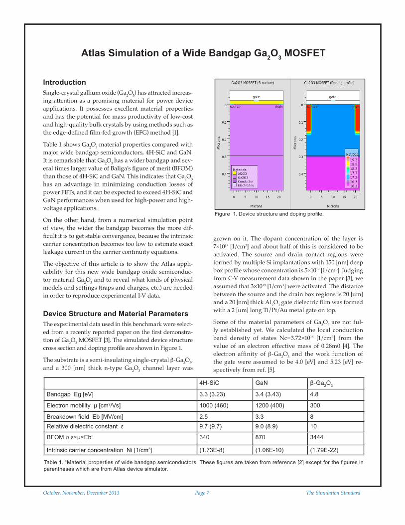
Figure 1. Device structure and doping profile.
4H-SiC GaN β-Ga2O3
Bandgap Eg [eV] 3.3 (3.23) 3.4 (3.43) 4.8
Electron mobility μ [cm2/Vs] 1000 (460) 1200 (400) 300
Breakdown field Eb [MV/cm] 2.5 3.3 8Relative dielectric constant ε 9.7 (9.7) 9.0 (8.9) 10
BFOM a ε×μ×Eb3 340 870 3444
Intrinsic carrier concentration Ni [1/cm3] (1.73E-8) (1.06E-10) (1.79E-22)
Table 1. “Material properties of wide bandgap semiconductors. These figures are taken from reference [2] except for the figures in parentheses which are from Atlas device simulator.
IntroductionSingle-crystal gallium oxide (Ga2O3) has attracted increas-ing attention as a promising material for power device applications. It possesses excellent material properties and has the potential for mass productivity of low-cost and high-quality bulk crystals by using methods such as the edge-defined film-fed growth (EFG) method [1].
Table 1 shows Ga2O3 material properties compared with major wide bandgap semiconductors, 4H-SiC and GaN. It is remarkable that Ga2O3 has a wider bandgap and sev-eral times larger value of Baliga’s figure of merit (BFOM) than those of 4H-SiC and GaN. This indicates that Ga2O3 has an advantage in minimizing conduction losses of power FETs, and it can be expected to exceed 4H-SiC and GaN performances when used for high-power and high-voltage applications.
On the other hand, from a numerical simulation point of view, the wider the bandgap becomes the more dif-ficult it is to get stable convergence, because the intrinsic carrier concentration becomes too low to estimate exact leakage current in the carrier continuity equations.
The objective of this article is to show the Atlas appli-cability for this new wide bandgap oxide semiconduc-tor material Ga2O3 and to reveal what kinds of physical models and settings (traps and charges, etc.) are needed in order to reproduce experimental I-V data.
Device Structure and Material ParametersThe experimental data used in this benchmark were select-ed from a recently reported paper on the first demonstra-tion of Ga2O3 MOSFET [3]. The simulated device structure cross section and doping profile are shown in Figure 1.
The substrate is a semi-insulating single-crystal β-Ga2O3, and a 300 [nm] thick n-type Ga2O3 channel layer was
grown on it. The dopant concentration of the layer is 7×10¹⁷ [1/cm3] and about half of this is considered to be activated. The source and drain contact regions were formed by multiple Si implantations with 150 [nm] deep box profile whose concentration is 5×10¹⁹ [1/cm3]. Judging from C-V measurement data shown in the paper [3], we assumed that 3×10¹⁹ [1/cm3] were activated. The distance between the source and the drain box regions is 20 [um] and a 20 [nm] thick Al2O3 gate dielectric film was formed with a 2 [um] long Ti/Pt/Au metal gate on top.
Some of the material parameters of Ga2O3 are not ful-ly established yet. We calculated the local conduction band density of states Nc=3.72×10¹⁸ [1/cm3] from the value of an electron effective mass of 0.28m0 [4]. The electron affinity of β-Ga2O3 and the work function of the gate were assumed to be 4.0 [eV] and 5.23 [eV] re-spectively from ref. [5].
The Simulation Standard Page 8 October, November, December 2013
We selected simple device models as much as possible. Only the LAT.TEMP parameter was set on the MODEL statement to solve the heat flow in the device and a con-stant thermal conductivity model was used. A basic constant low-field mobility model was selected with the lattice temperature coefficient for the temperature de-pendence of electron mobility TMUN=2.0 in equation (1).
(1)
Other parameters used for fittings are shown in Table 2.
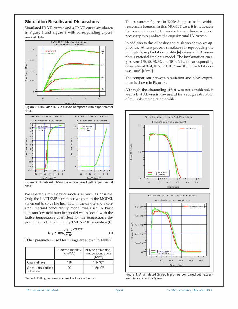
Figure 2. Simulated ID-VD curves compared with experimental data.
Figure 3. Simulated ID-VG curve compared with experimental data.
Electron mobility [cm2/Vs]
N-type active dop-ant concentration
[1/cm3]
Channel layer 118 1.1×10¹⁷
Semi - insulat ing substrate
20 1.5x10¹⁶
Table 2. Fitting parameters used in this simulation.Figure 4. A simulated Si depth profiles compared with experi-ment is show in this figure.
Simulation Results and DiscussionsSimulated ID-VD curves and a ID-VG curve are shown in Figure 2 and Figure 3 with corresponding experi-mental data.
The parameter figures in Table 2 appear to be within reasonable bounds. In this MOSFET case, it is noticeable that a complex model, trap and interface charge were not necessary to reproduce the experimental I-V curves.
In addition to the Atlas device simulation above, we ap-plied the Athena process simulator for reproducing the multiple Si implantation profile [6] using a BCA amor-phous material implants model. The implantation ener-gies were 175, 95, 60, 30, and 10 [keV] with corresponding dose ratio of 0.64, 0.15, 0.11, 0.07 and 0.03. The total dose was 1×10¹⁵ [1/cm2].
The comparison between simulation and SIMS experi-ment is shown in Figure 4.
Although the channeling effect was not considered, it seems that Athena is also useful for a rough estimation of multiple implantation profile.

October, November, December 2013 Page 9 The Simulation Standard
ConclusionWe demonstrated Atlas device simulation of a Ga2O3 MOSFET’s DC and transfer characteristics. Fairly good agreements with experimental data were obtained using constant mobility model even without any defect trap and interface charge. Also, Athena BCA Monte Carlo implantation simulation was applied to simulate dop-ing profiles successfully. In view of these results, Ga2O3 is a promising material free from serious crystal defects which are suitable for device fabrication, and expected to surpass 4H-SiC and GaN materials in power device applications.
References[1]. H. Aida, K. Nishiguchi, H. Takeda, N. Aota, K. Sunakawa and Y.
Yaguchi,“Growth of β-Ga2O3 Single Crystals by the Edge-Defined, Film Fed Growth Method”, Jpn. J. Appl. Phys. 47, 8506(2008).
[2]. M. Higashiwaki, K. Sasaki, A. Kuramata, T. Masui and S. Yama-koshi, “Gallium oxide (Ga2O3) metal-semiconductor field-effect transistors on single-crystal β-Ga2O3(010) substrates”, Appl. Phys. Lett. 100, 013504 (2012).
[3]. M.Higashiwaki, K. Sasaki, T. Kamimura, M. H. Wong, D. Krishna-murthy, A. Kuramata, T. Masui and S. Yamakoshi,”Depletion-mode Ga2O3 MOSFETs”, 71st Annual Device Research Conference (DRC), 10.1109/DRC.2013.6633890.
[4]. K. Irmscher, Z. Galazka, M. Pietsch, R. Uecher, and R. Fornari, “Electrical properties of β-Ga2O3 single crystals grown by the Czo-chralski method”, J. Appl. Phys. 110, 063720 (2011).
[5]. M. Mohamed, K. Irmscher, C. Jannowitz, Z. Galazka, R. Manzke, and R. Fornari, “Schottky barrier height of Au on transparent semi-conducting oxide β-Ga2O3”, Appl. Phys. Lett. 101, 132106 (2012).
[6]. K. Sasaki, M. Higashiwaki, A. Kuramata, T. Masui and S. Yamako-shi, “Si-Ion Implantation Doping in β-Ga2O3 and Its Application to Fabrication of Low-Resistance Ohmic Contacts”, Appl. Phys. Exp. 6, 086502 (2013).


![UCSUCSBUCSB - University of California, Santa Barbara · BFOM = Baliga’s figure of merit for power transistor performance [K*µ*Ec3] JFM = Johnson’s figure of merit for power](https://static.fdocument.org/doc/165x107/5b50d8ea7f8b9ac4368b6a80/ucsucsbucsb-university-of-california-santa-barbara-bfom-baligas-figure.jpg)