A1656A165 125nA nanoPoer Sperisor Circits it ... · SWT Ramp Threshold VRAMP2 VCC = 1.6V to 5V...
17
General Description The MAX16056–MAX16059 are ultra-low-current 125nA (typ) microprocessor (μP) supervisory circuits that moni- tor a single system supply voltage. These devices assert an active-low reset signal whenever the V CC supply voltage drops below the factory-trimmed reset threshold, manual reset is pulled low, or the watchdog timer runs out (MAX16056/MAX16058). The reset output remains asserted for an adjustable reset timeout period after V CC rises above the reset threshold. Factory-trimmed reset threshold voltages are offered from 1.575V to 4.625V in approximately 100mV increments (see Table 1). These devices feature adjustable reset and watchdog timeout using external capacitors. The MAX16056/ MAX16058 contain a watchdog timer with a watchdog select input (WDS) that multiplies the watchdog timeout period by 128. The MAX16057/MAX16059 do not have the watchdog feature. The MAX16056–MAX16059 are available in either push- pull or open-drain output-type configurations (see the Ordering Information). These devices are fully specified over the -40°C to +125°C automotive temperature range. The MAX16056/MAX16058 are available in an 8-pin TDFN package, and the MAX16057/MAX16059 are avail- able in a 6-pin TDFN package. Applications ● Portable/Battery-Powered Equipment ● PDAs/Cell Phones ● MP3 Players/Pagers ● Glucose Monitors/Patient Monitors ● Metering/HVAC Benefits and Features ● Reduced Power Requirements • Ultra-Low 125nA (typ) Supply Current • 1.1V to 5.5V Operating Supply Range ● Configurable Circuit Enables Flexible Designs • Factory-Set Reset Threshold Options from 1.575V to 4.625V in Approximately 100mV Increments • Capacitor-Adjustable Reset Timeout • Capacitor-Adjustable Watchdog Timeout (MAX16056/MAX16058) • Watchdog Timer Capacitor Open Detect Function • Optional Watchdog Disable Function (MAX16056/ MAX16058) • Manual-Reset Input • Push-Pull or Open-Drain RESET Output Options ● Integrated Features Increases System Robustness • Power-Supply Transient Immunity • Guaranteed RESET Valid for V CC ≥ 1.1V ● Saves Board Space • 3mm x 3mm TDFN Package Typical Operating Circuit and Ordering Information appear at end of data sheet. 19-4686; Rev 5; 3/17 1 1 2 3 6 5 4 3 4 8 6 5 VCC WDI SRT MAX16056 MAX16058 MAX16057 MAX16059 2 7 WDS VCC SRT N.C. RESET SWT EP EP MR GND TDFN TOP VIEW TDFN RESET *CONNECT EXPOSED PAD TO GND. MR GND Pin Configurations MAX16056–MAX16059 125nA nanoPower Supervisory Circuits with Capacitor-Adjustable Reset and Watchdog Timeouts
Transcript of A1656A165 125nA nanoPoer Sperisor Circits it ... · SWT Ramp Threshold VRAMP2 VCC = 1.6V to 5V...
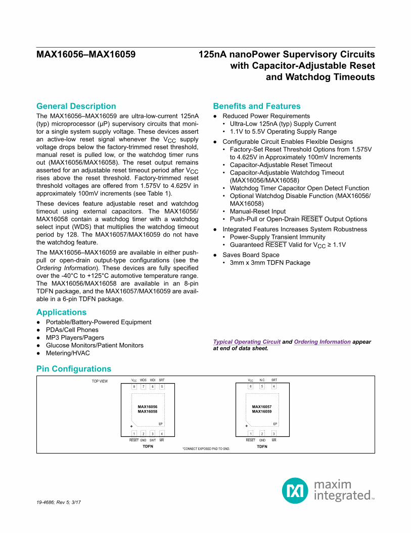
General DescriptionThe MAX16056–MAX16059 are ultra-low-current 125nA (typ) microprocessor (μP) supervisory circuits that moni-tor a single system supply voltage. These devices assert an active-low reset signal whenever the VCC supply voltage drops below the factory-trimmed reset threshold, manual reset is pulled low, or the watchdog timer runs out (MAX16056/MAX16058). The reset output remains asserted for an adjustable reset timeout period after VCC rises above the reset threshold. Factory-trimmed reset threshold voltages are offered from 1.575V to 4.625V in approximately 100mV increments (see Table 1).These devices feature adjustable reset and watchdog timeout using external capacitors. The MAX16056/MAX16058 contain a watchdog timer with a watchdog select input (WDS) that multiplies the watchdog timeout period by 128. The MAX16057/MAX16059 do not have the watchdog feature.The MAX16056–MAX16059 are available in either push-pull or open-drain output-type configurations (see the Ordering Information). These devices are fully specified over the -40°C to +125°C automotive temperature range. The MAX16056/MAX16058 are available in an 8-pin TDFN package, and the MAX16057/MAX16059 are avail-able in a 6-pin TDFN package.
Applications Portable/Battery-Powered Equipment PDAs/Cell Phones MP3 Players/Pagers Glucose Monitors/Patient Monitors Metering/HVAC
Benefits and Features Reduced Power Requirements
• Ultra-Low 125nA (typ) Supply Current• 1.1V to 5.5V Operating Supply Range
Configurable Circuit Enables Flexible Designs• Factory-Set Reset Threshold Options from 1.575V
to 4.625V in Approximately 100mV Increments• Capacitor-Adjustable Reset Timeout• Capacitor-Adjustable Watchdog Timeout
(MAX16056/MAX16058)• Watchdog Timer Capacitor Open Detect Function• Optional Watchdog Disable Function (MAX16056/
MAX16058)• Manual-Reset Input• Push-Pull or Open-Drain RESET Output Options
Integrated Features Increases System Robustness• Power-Supply Transient Immunity• Guaranteed RESET Valid for VCC ≥ 1.1V
Saves Board Space• 3mm x 3mm TDFN Package
Typical Operating Circuit and Ordering Information appear at end of data sheet.
19-4686; Rev 5; 3/17
1 1 2 3
6 5 4
3 4
8 6 5
VCC WDI SRT
MAX16056MAX16058
MAX16057MAX16059
2
7
WDS VCC SRTN.C.
RESET SWT
EP EP
MRGND
TDFN
TOP VIEW
TDFNRESET
*CONNECT EXPOSED PAD TO GND.
MRGND
Pin Configurations
MAX16056–MAX16059 125nA nanoPower Supervisory Circuits with Capacitor-Adjustable Reset
and Watchdog Timeouts
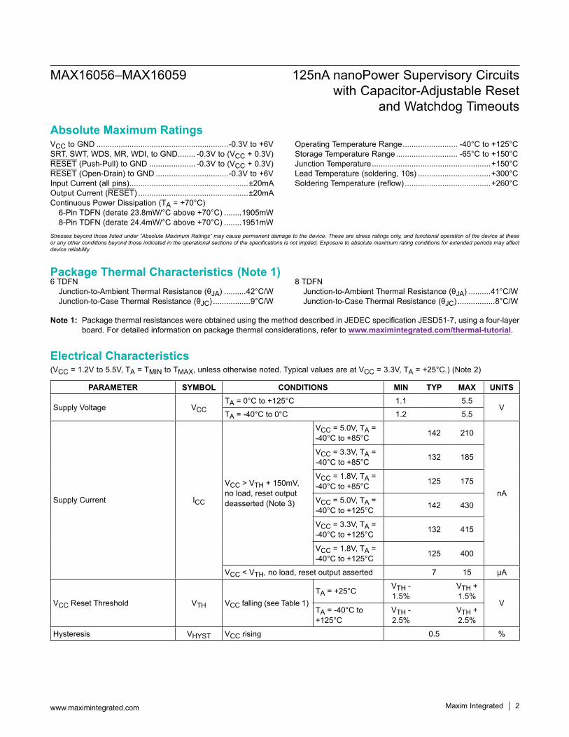
VCC to GND ............................................................-0.3V to +6VSRT, SWT, WDS, MR, WDI, to GND ........ -0.3V to (VCC + 0.3V)RESET (Push-Pull) to GND ..................... -0.3V to (VCC + 0.3V)RESET (Open-Drain) to GND .................................-0.3V to +6VInput Current (all pins) ......................................................±20mAOutput Current (RESET) ..................................................±20mAContinuous Power Dissipation (TA = +70°C)
6-Pin TDFN (derate 23.8mW/°C above +70°C) ........1905mW 8-Pin TDFN (derate 24.4mW/°C above +70°C) ........1951mW
Operating Temperature Range ......................... -40°C to +125°CStorage Temperature Range ............................ -65°C to +150°CJunction Temperature ......................................................+150°CLead Temperature (soldering, 10s) .................................+300°CSoldering Temperature (reflow) .......................................+260°C
6 TDFN Junction-to-Ambient Thermal Resistance (θJA) ..........42°C/W
Junction-to-Case Thermal Resistance (θJC) .................9°C/W
8 TDFN Junction-to-Ambient Thermal Resistance (θJA) ..........41°C/W Junction-to-Case Thermal Resistance (θJC) .................8°C/W
(Note 1)
(VCC = 1.2V to 5.5V, TA = TMIN to TMAX, unless otherwise noted. Typical values are at VCC = 3.3V, TA = +25°C.) (Note 2)
Note 1: Package thermal resistances were obtained using the method described in JEDEC specification JESD51-7, using a four-layer board. For detailed information on package thermal considerations, refer to www.maximintegrated.com/thermal-tutorial.
Absolute Maximum Ratings
Stresses beyond those listed under “Absolute Maximum Ratings” may cause permanent damage to the device. These are stress ratings only, and functional operation of the device at these or any other conditions beyond those indicated in the operational sections of the specifications is not implied. Exposure to absolute maximum rating conditions for extended periods may affect device reliability.
Electrical Characteristics
Package Thermal Characteristics
PARAMETER SYMBOL CONDITIONS MIN TYP MAX UNITS
Supply Voltage VCCTA = 0°C to +125°C 1.1 5.5
VTA = -40°C to 0°C 1.2 5.5
Supply Current ICC
VCC > VTH + 150mV,no load, reset output deasserted (Note 3)
VCC = 5.0V, TA = -40°C to +85°C 142 210
nA
VCC = 3.3V, TA = -40°C to +85°C 132 185
VCC = 1.8V, TA = -40°C to +85°C 125 175
VCC = 5.0V, TA = -40°C to +125°C 142 430
VCC = 3.3V, TA = -40°C to +125°C 132 415
VCC = 1.8V, TA = -40°C to +125°C 125 400
VCC < VTH, no load, reset output asserted 7 15 µA
VCC Reset Threshold VTH VCC falling (see Table 1)TA = +25°C VTH -
1.5%VTH + 1.5%
VTA = -40°C to +125°C
VTH - 2.5%
VTH + 2.5%
Hysteresis VHYST VCC rising 0.5 %
MAX16056–MAX16059 125nA nanoPower Supervisory Circuits with Capacitor-Adjustable Reset
and Watchdog Timeouts
www.maximintegrated.com Maxim Integrated 2
(VCC = 1.2V to 5.5V, TA = TMIN to TMAX, unless otherwise noted. Typical values are at VCC = 3.3V, TA = +25°C.) (Note 2)
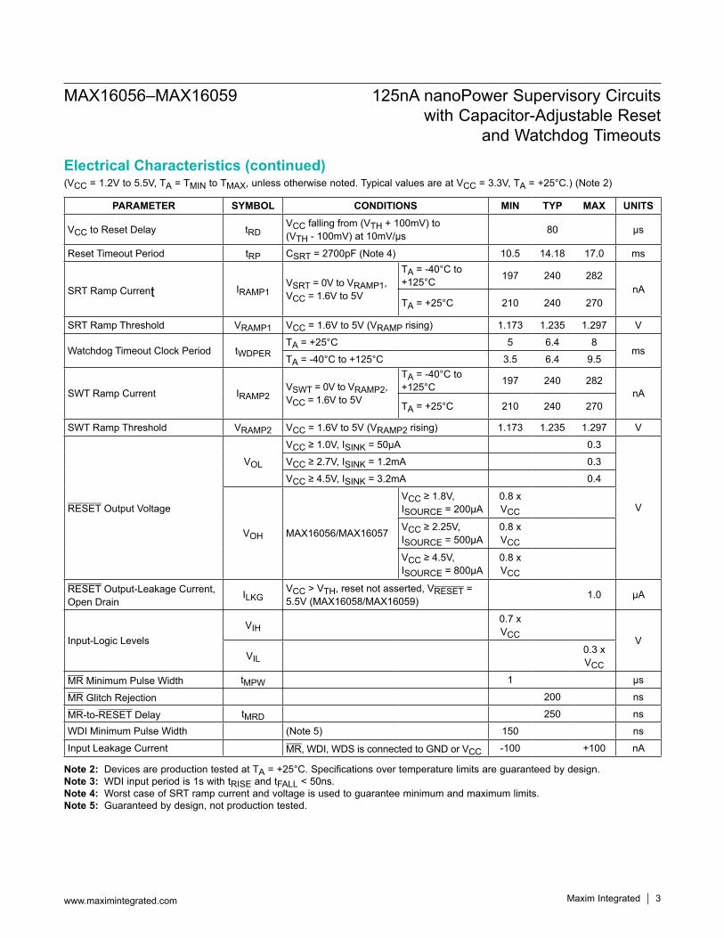
Note 2: Devices are production tested at TA = +25°C. Specifications over temperature limits are guaranteed by design.Note 3: WDI input period is 1s with tRISE and tFALL < 50ns.Note 4: Worst case of SRT ramp current and voltage is used to guarantee minimum and maximum limits.Note 5: Guaranteed by design, not production tested.
Electrical Characteristics (continued)
PARAMETER SYMBOL CONDITIONS MIN TYP MAX UNITS
VCC to Reset Delay tRDVCC falling from (VTH + 100mV) to(VTH - 100mV) at 10mV/µs 80 µs
Reset Timeout Period tRP CSRT = 2700pF (Note 4) 10.5 14.18 17.0 ms
SRT Ramp Current IRAMP1VSRT = 0V to VRAMP1, VCC = 1.6V to 5V
TA = -40°C to +125°C 197 240 282
nATA = +25°C 210 240 270
SRT Ramp Threshold VRAMP1 VCC = 1.6V to 5V (VRAMP rising) 1.173 1.235 1.297 V
Watchdog Timeout Clock Period tWDPERTA = +25°C 5 6.4 8
msTA = -40°C to +125°C 3.5 6.4 9.5
SWT Ramp Current IRAMP2VSWT = 0V to VRAMP2, VCC = 1.6V to 5V
TA = -40°C to +125°C 197 240 282
nATA = +25°C 210 240 270
SWT Ramp Threshold VRAMP2 VCC = 1.6V to 5V (VRAMP2 rising) 1.173 1.235 1.297 V
RESET Output Voltage
VOL
VCC ≥ 1.0V, ISINK = 50µA 0.3
V
VCC ≥ 2.7V, ISINK = 1.2mA 0.3
VCC ≥ 4.5V, ISINK = 3.2mA 0.4
VOH MAX16056/MAX16057
VCC ≥ 1.8V, ISOURCE = 200µA
0.8 x VCC
VCC ≥ 2.25V, ISOURCE = 500µA
0.8 x VCC
VCC ≥ 4.5V, ISOURCE = 800µA
0.8 x VCC
RESET Output-Leakage Current, Open Drain
ILKGVCC > VTH, reset not asserted, VRESET = 5.5V (MAX16058/MAX16059)
1.0 µA
Input-Logic LevelsVIH
0.7 x VCC V
VIL0.3 x VCC
MR Minimum Pulse Width tMPW 1 µs
MR Glitch Rejection 200 ns
MR-to-RESET Delay tMRD 250 ns
WDI Minimum Pulse Width (Note 5) 150 ns
Input Leakage Current MR, WDI, WDS is connected to GND or VCC -100 +100 nA
MAX16056–MAX16059 125nA nanoPower Supervisory Circuits with Capacitor-Adjustable Reset
and Watchdog Timeouts
www.maximintegrated.com Maxim Integrated 3
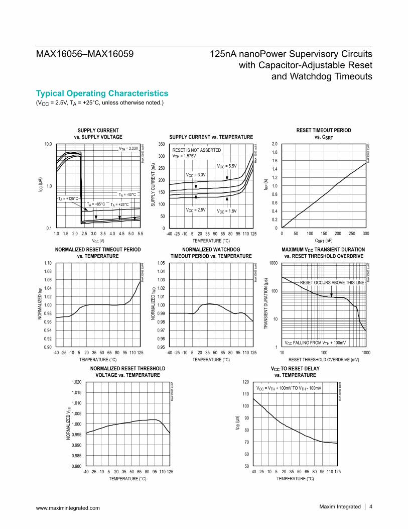
(VCC = 2.5V, TA = +25°C, unless otherwise noted.)Typical Operating Characteristics
SUPPLY CURRENT vs. TEMPERATURE
MAX
1605
6 to
c02
TEMPERATURE (°C)
SUPP
LY C
URRE
NT (n
A)
1109580655035205-10-25
50
100
150
200
250
300
350
0-40 125
RESET IS NOT ASSERTEDVTH = 1.575V
VCC = 3.3V
VCC = 2.5V
VCC = 5.5V
VCC = 1.8V
RESET TIMEOUT PERIODvs. CSRT
MAX
1605
6 to
c03
CSRT (nF)
t RP (
s)
25020015010050
0.2
0.4
0.6
0.8
1.0
1.2
1.4
1.6
1.8
2.0
00 300
NORMALIZED RESET TIMEOUT PERIODvs. TEMPERATURE
MAX
1605
6 to
c04
TEMPERATURE (°C)
NORM
ALIZ
ED t R
P
1109565 80-10 5 20 35 50-25
0.92
0.94
0.96
0.98
1.00
1.02
1.04
1.06
1.08
1.10
0.90-40 125
NORMALIZED WATCHDOGTIMEOUT PERIOD vs. TEMPERATURE
MAX
1605
6 to
c05
TEMPERATURE (°C)
NORM
ALIZ
ED t W
D
1109565 80-10 5 20 35 50-25
0.96
0.97
0.98
0.99
1.00
1.01
1.02
1.03
1.04
1.05
0.95-40 125
MAXIMUM VCC TRANSIENT DURATION vs. RESET THRESHOLD OVERDRIVE
MAX
1605
6 to
c06
RESET THRESHOLD OVERDRIVE (mV)
TRAN
SIEN
T DU
RATI
ON (µ
s)
100
10
100
1000
110 1000
RESET OCCURS ABOVE THIS LINE
VCC FALLING FROM VTH + 100mV
NORMALIZED RESET THRESHOLDVOLTAGE vs. TEMPERATURE
MAX
1605
6 to
c07
TEMPERATURE (°C)
NORM
ALIZ
ED V
TH
11095-25 -10 5 35 50 6520 80
0.985
0.990
0.995
1.000
1.005
1.010
1.015
1.020
0.980-40 125
SUPPLY CURRENTvs. SUPPLY VOLTAGE
MAX
1605
6 to
c01
VCC (V)
I CC
(µA)
3.5 4.0 4.5 5.0
10.0
1.0
0.11.0 1.5 2.0 2.5 3.0 5.5
VTH = 2.23V
TA = +125°CTA = +85°C TA = +25°C
TA = -40°C
VCC TO RESET DELAYvs. TEMPERATURE
MAX
1605
6 to
c08
TEMPERATURE (°C)
t RD
(µs)
1109580655035205-10-25
60
70
80
90
100
110
120
50-40 125
VCC = VTH + 100mV TO VTH - 100mV
MAX16056–MAX16059 125nA nanoPower Supervisory Circuits with Capacitor-Adjustable Reset
and Watchdog Timeouts
Maxim Integrated 4www.maximintegrated.com
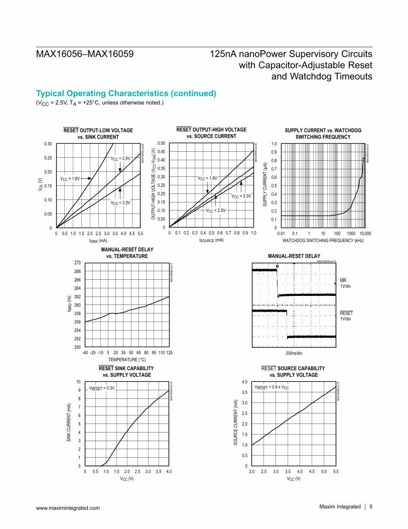
(VCC = 2.5V, TA = +25°C, unless otherwise noted.)Typical Operating Characteristics (continued)
RESET OUTPUT-LOW VOLTAGEvs. SINK CURRENT
MAX
1605
6 to
c09
ISINK (mA)
V OL (
V)
4.54.03.53.02.52.01.51.00.5
0.05
0.10
0.15
0.20
0.25
0.30
00 5.0
VCC = 1.8V
VCC = 2.5V
VCC = 3.3V
RESET OUTPUT-HIGH VOLTAGEvs. SOURCE CURRENT
MAX
1605
6 to
c10
ISOURCE (mA)
OUTP
UT-H
IGH
VOLT
AGE
(VCC
-VOH
) (V)
0.05
0.10
0.15
0.20
0.25
0.30
0.35
0.40
0.45
0.50
00.90.80.6 0.70.2 0.3 0.4 0.50.10 1.0
VCC = 1.8V
VCC = 2.5V
VCC = 3.3V
SUPPLY CURRENT vs. WATCHDOGSWITCHING FREQUENCY
MAX
1605
6 to
c11
WATCHDOG SWITCHING FREQUENCY (kHz)
SUPP
LY C
URRE
NT (µ
A)
10001001010.1
0.4
0.3
0.5
0.6
0.7
0.8
0.9
1.0
0.2
0.1
00.01 10,000
MANUAL-RESET DELAYvs. TEMPERATURE
MAX
1605
6 to
c12
TEMPERATURE (°C)
t MRD
(ns)
1109565 80-10 5 20 35 50-25
252
254
256
258
260
262
264
266
268
270
250-40 125
MANUAL-RESET DELAYMAX16056 toc13
RESET1V/div
MR1V/div
200ns/div
RESET SINK CAPABILITY vs. SUPPLY VOLTAGE
MAX
1605
6 to
c14
VCC (V)
SINK
CUR
RENT
(mA)
3.53.02.0 2.51.0 1.50.5
1
2
3
4
5
6
7
8
9
10
00 4.0
VRESET = 0.3V
RESET SOURCE CAPABILITY vs. SUPPLY VOLTAGE
MAX
1605
6 to
c15
VCC (V)
SOUR
CE C
URRE
NT (m
A)
5.04.52.5 3.0 3.5 4.0
0.5
1.0
1.5
2.0
2.5
3.0
3.5
4.0
02.0 5.5
VRESET = 0.8 x VCC
MAX16056–MAX16059 125nA nanoPower Supervisory Circuits with Capacitor-Adjustable Reset
and Watchdog Timeouts
Maxim Integrated 5www.maximintegrated.com
Note 6: Floor: take the integral value.
Pin DescriptionPIN
NAME FUNCTIONMAX16056/MAX16058
MAX16057/MAX16059
1 1 RESET
Push-Pull or Open-Drain Reset Output. RESET asserts whenever VCC drops below the selected reset threshold voltage (VTH) or manual reset is pulled low. RESET remains low for the reset timeout period after all reset conditions are deasserted, and then goes high. The watchdog timer triggers a reset pulse (tRP) whenever a watchdog fault occurs (MAX16056/MAX16058).
2 2 GND Ground
3 — SWT
Watchdog Timeout Input. Connect a capacitor between SWT and GND to set the basic watchdog timeout period (tWD). Determine the period by the formula tWD = Floor[CSWT x 5.15 x 10⁶/6.4ms] x 6.4ms + 3.2ms (Note 6) with tWD in seconds and CSWT in Farads, or use Table 2. Extend the basic watchdog timeout period by using the WDS input. Connect SWT to ground to disable the watchdog timer function. The value of the capacitor must be between 2275pF and 0.54µF to have a valid watchdog timeout period.
4 3 MRManual-Reset Input. Drive MR low to manually reset the device. RESET remains asserted for the reset timeout period after MR is released. There is no internal pullup on MR. MR must not be left unconnected. Connect MR to VCC if not used.
5 4 SRT
Reset Timeout Input. Connect a capacitor from SRT to GND to select the reset timeout period. Determine the period as follows: tRP = 5.15 x 10⁶ x CSRT with tRP in seconds and CSRT in Farads, or use Table 2. The value of the capacitor must be between 39pF and 4.7µF.
6 — WDI
Watchdog Input. A falling transition must occur on WDI within the selected watchdog timeout period or a reset pulse occurs. The watchdog timer clears when a falling transition occurs on WDI or whenever RESET is asserted. Connect SWT to ground to disable the watchdog timer function.
7 — WDS
Watchdog Select Input. WDS selects the watchdog timeout mode. Connect WDS to ground to select normal mode. The watchdog timeout period is tWD. Connect WDS to VCC to select extended mode, multiplying the basic timeout period (tWD) by a factor of 128. A change in the state of WDS clears the watchdog timer.
8 6 VCCSupply Voltage. VCC is the power-supply input and the input for fixed-threshold VCC monitor. For noisy systems, bypass VCC with a 0.1µF capacitor to GND.
— 5 N.C. No Connection. Not internally connected.
— — EP Exposed Pad. Connect EP to GND or leave unconnected.
MAX16056–MAX16059 125nA nanoPower Supervisory Circuits with Capacitor-Adjustable Reset
and Watchdog Timeouts
www.maximintegrated.com Maxim Integrated 6
Detailed DescriptionThe MAX16056–MAX16059 are ultra-low-current 125nA (typ) μP supervisory circuits that monitor a single system supply voltage. These devices assert an active-low reset signal whenever the VCC supply voltage drops below the factory-trimmed reset threshold, manual reset is pulled low, or the watchdog timer runs out (MAX16056/MAX16058). The reset output remains asserted for an adjustable reset timeout period after VCC rises above the reset threshold. The reset and watchdog delay periods are adjustable using external capacitors.
RESET OutputThe MAX16056–MAX16059 μP supervisory circuits assert a reset to prevent code-execution errors during power-up, power-down, and brownout conditions. The reset output is guaranteed to be valid for VCC down to 1.1V.When VCC falls below the reset threshold, the RESET output asserts low. Once VCC exceeds the reset thresh-old plus the hysteresis, an internal timer keeps the RESET output asserted for the capacitor-adjusted reset timeout period (tRP), then after this interval the RESET output deasserts (Figure 1). The reset function features immunity to power-supply voltage transients.
Manual-Reset Input (MR)Many μP-based products require manual-reset capability, allowing the operator, a test technician, or external logic circuitry to initiate a reset. The MAX16056–MAX16059 feature an MR input. A logic-low on MR asserts a reset. RESET remains asserted while MR is low and for the timeout period (tRP)after MR returns high. Connect MR to VCC if unused. MR can be driven with CMOS logic levels or with open-drain/collector outputs (with a pullup resis-tor). Connect a normally open momentary switch from MR to GND and a resistor from MR to VCC to implement a manual-reset function; external debounce circuitry is not required. If MR is driven by long cables or the device is used in a noisy environment, connect a 0.1μF capacitor from MR to GND to provide additional noise immunity.
Watchdog TimerThe MAX16056/MAX16058’s watchdog timer circuitry monitors the μP’s activity. If the μP does not tog-gle (high to low) the watchdog input (WDI) within the capacitor-adjustable watchdog timeout period (tWD), RESET asserts for the reset timeout period (tRP). The internal watchdog timer is cleared by: 1) any event that asserts RESET, 2) a falling transition at WDI (that can detect pulses as short as 150ns), or 3) a transition (high to low or low to high) at WDS. While RESET is asserted, the watchdog timer remains cleared and does not count. As soon as RESET deasserts, the watchdog timer resumes counting.There are two modes of watchdog operation, normal mode and extended mode. In normal mode (Figure 2), the watchdog timeout period is determined by the value of the capacitor connected between SWT and ground. In extended mode (Figure 3), the watchdog timeout period is multiplied by 128. For example, in extended mode, a 0.33μF capacitor gives a watchdog timeout period of 217s (Table 2). To disable the watchdog timer function, connect SWT to ground.When VCC ramps above VTH + VHYST, the value of the external SWT capacitor is sampled after RESET goes high. When sampling is finished, the capacitor value is stored in the device and is used to set watchdog timeout. If RESET goes low before sampling is finished, the device interrupts sampling, and sampling is restarted when RESET goes high again.If the external SWT capacitor is less than 470pF, the sampling result sets the watchdog timeout to zero. This causes the watchdog to assert RESET continuously after sampling is finished. If a PCB manufacturing defect caused the connection to CSWT to be broken, the capacitance is very low and RESET is continuously asserted. If the external SWT capacitor is greater than 0.47μF, the sampling result sets the watchdog timeout to be infinite, disabling the watchdog function.
MAX16056–MAX16059 125nA nanoPower Supervisory Circuits with Capacitor-Adjustable Reset
and Watchdog Timeouts
www.maximintegrated.com Maxim Integrated 7
Figure 1. RESET Timing Relationship
Figure 2. Watchdog Timing Diagram, Normal Mode (WDS = GND)
Figure 3. Watchdog Timing Diagram, Extended Mode (WDS = VCC)
VCC
tRPtRP
tMRD
tMPW
tRD
VTH + VHYST
RESET
MR
VTH
tWD tRP
VCC
VCC
0V
0V
WDI
RESET
NORMAL MODE (WDS = GND)
tWD x 128
tRP
VCC
VCC
0V
0V
WDI
RESET
EXTENDED MODE (WDS = VCC)
MAX16056–MAX16059 125nA nanoPower Supervisory Circuits with Capacitor-Adjustable Reset
and Watchdog Timeouts
www.maximintegrated.com Maxim Integrated 8
Applications InformationSelecting the Reset Timeout CapacitorThe reset timeout period is adjustable to accommodate a variety of μP applications. To adjust the reset timeout period (tRP), connect a capacitor (CSRT) between SRT and ground. The reset timeout capacitor is calculated as follows:
CSRT = tRP/(5.15 x 106)with tRP in seconds and CSRT in Farads.CSRT must be a low-leakage (< 10nA) type capacitor. A ceramic capacitor with low temperature coefficient dielectric (i.e., X7R) is recommended.
Selecting Watchdog Timeout CapacitorThe watchdog timeout period is adjustable to accommodate a variety of μP applications. With this feature, the watchdog timeout can be optimized for software execution. The programmer can determine how often the watchdog timer should be serviced. Adjust the watchdog timeout period (tWD) by connecting a capacitor (CSWT) between SWT and GND. For normal mode operation, calculate the watchdog timeout as follows: tWD = Floor[CSWT x 5.15 x 10⁶/6.4ms] x 6.4ms + 3.2ms
with tWD in seconds and CSWT in Farads. (Floor: take the integral value) (Figures 2 and 3)The maximum tWD is 296s. If the capacitor sets tWD greater than the 296s, tWD = infinite and the watchdog timer is disabled.CSWT must be a low-leakage (< 10nA) type capacitor. A ceramic capacitor with low temperature coefficient dielectric (i.e., X7R) is recommended.
Watchdog Timeout AccuracyThe watchdog timeout period is affected by the SWT ramp current (IRAMP2) accuracy, the SWT ramp thresh-old (VRAMP2), and the watchdog timeout clock period (tWDPER). In the equation above, the constant 5.15 x 10⁶ is equal to VRAMP2/IRAMP2, and 6.4ms equals the watch-dog timeout clock period. Calculate the timeout accuracy
by substituting the minimum, typical, and maximum values into the equation.For example, if CSWT = 100nF:tWDMIN = Floor[100 x 10-9 x 1.173/(282 x 10-9)/9.5ms] x 3.5ms + 0.5 x 3.2ms = 141.7mstWDNOM = Floor[100 x 10-9 x 1.235/(240 x 10-9)/6.4ms] x 6.4ms + 0.5 x 6.4ms = 515.2mstWDMAX = Floor[100 x 10-9 x 1.297/(197 x 10-9)/3.5ms] x 9.5ms + 0.5 x 9.5ms = 1790.75ms
Transient ImmunityFor applications with higher slew rates on VCC during power-up, additional bypass capacitance may be required.The MAX16056–MAX16059 are relatively immune to short-duration supply voltage transients, or glitches on VCC. The Maximum VCC Transient Duration vs. Reset Threshold Overdrive graph in the Typical Operating Characteristics shows this transient immunity. The area below the curve of the graph is the region where these devices typically do not generate a reset pulse. This graph was generated using a falling pulse applied to VCC, starting 100mV above the actual reset threshold (VTH), and ending below this threshold (reset threshold overdrive). As the magnitude of the transient increases, the maximum allowable pulse width decreases. Typically, a 100mV VCC transient duration of 40μs or less does not cause a reset.
Using the MAX16056–MAX16059 for Reducing System Power ConsumptionUsing the RESET output to control an external p-channel MOSFET to control the on-time of a power supply can result in lower system power consumption in systems that can be regularly put to sleep. By tying the WDI input to ground, the RESET output becomes a low-frequency clock output. When RESET is low, the MOSFET is turned on and power is applied to the system. When RESET is high, the MOSFET is turned off and no power is con-sumed by the system. This effectively reduces the shut-down current of the system to zero (Figure 4).
MAX16056–MAX16059 125nA nanoPower Supervisory Circuits with Capacitor-Adjustable Reset
and Watchdog Timeouts
www.maximintegrated.com Maxim Integrated 9
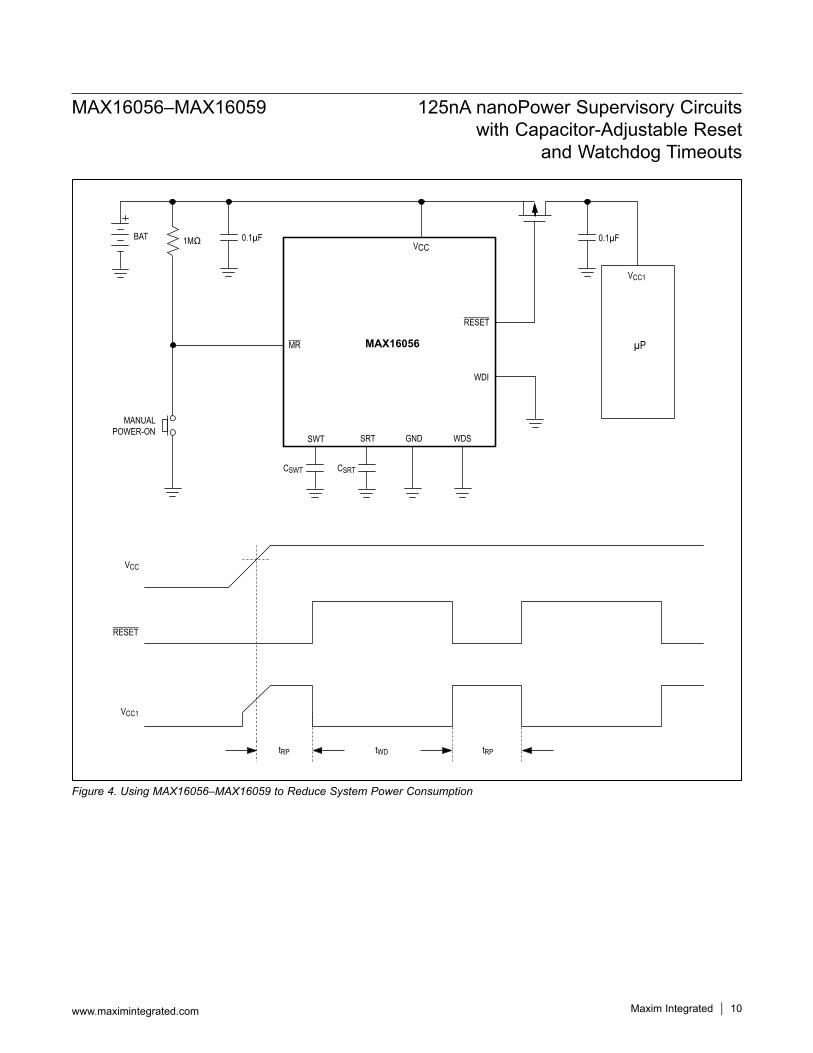
Figure 4. Using MAX16056–MAX16059 to Reduce System Power Consumption
MR
SWT SRT GND WDS
WDI
BAT 0.1µF0.1µF
µP
MANUALPOWER-ON
1MΩ
CSWT CSRT
MAX16056
RESET
VCC
VCC1
VCC
RESET
tRP
VCC1
tRPtWD
MAX16056–MAX16059 125nA nanoPower Supervisory Circuits with Capacitor-Adjustable Reset
and Watchdog Timeouts
www.maximintegrated.com Maxim Integrated 10
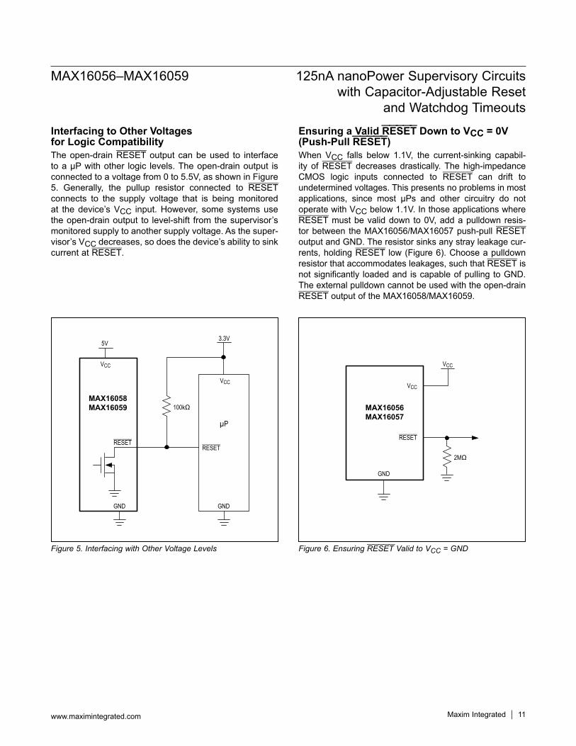
Interfacing to Other Voltages for Logic CompatibilityThe open-drain RESET output can be used to interface to a μP with other logic levels. The open-drain output is connected to a voltage from 0 to 5.5V, as shown in Figure 5. Generally, the pullup resistor connected to RESET connects to the supply voltage that is being monitored at the device’s VCC input. However, some systems use the open-drain output to level-shift from the supervisor’s monitored supply to another supply voltage. As the super-visor’s VCC decreases, so does the device’s ability to sink current at RESET.
Ensuring a Valid RESET Down to VCC = 0V (Push-Pull RESET)When VCC falls below 1.1V, the current-sinking capabil-ity of RESET decreases drastically. The high-impedance CMOS logic inputs connected to RESET can drift to undetermined voltages. This presents no problems in most applications, since most μPs and other circuitry do not operate with VCC below 1.1V. In those applications where RESET must be valid down to 0V, add a pulldown resis-tor between the MAX16056/MAX16057 push-pull RESET output and GND. The resistor sinks any stray leakage cur-rents, holding RESET low (Figure 6). Choose a pulldown resistor that accommodates leakages, such that RESET is not significantly loaded and is capable of pulling to GND. The external pulldown cannot be used with the open-drain RESET output of the MAX16058/MAX16059.
Figure 5. Interfacing with Other Voltage Levels Figure 6. Ensuring RESET Valid to VCC = GND
5V
GND
µP
RESET
100kΩ
3.3V
MAX16058MAX16059
VCC
VCC
GND
RESET
VCC
VCC
GND
RESET
2MΩ
MAX16056MAX16057
MAX16056–MAX16059 125nA nanoPower Supervisory Circuits with Capacitor-Adjustable Reset
and Watchdog Timeouts
www.maximintegrated.com Maxim Integrated 11
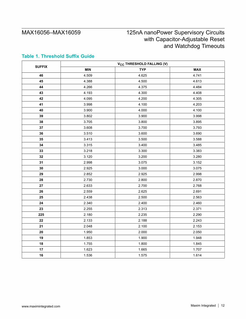
Table 1. Threshold Suffix Guide
SUFFIXVCC THRESHOLD FALLING (V)
MIN TYP MAX46 4.509 4.625 4.741
45 4.388 4.500 4.613
44 4.266 4.375 4.484
43 4.193 4.300 4.408
42 4.095 4.200 4.305
41 3.998 4.100 4.203
40 3.900 4.000 4.100
39 3.802 3.900 3.998
38 3.705 3.800 3.895
37 3.608 3.700 3.793
36 3.510 3.600 3.690
35 3.413 3.500 3.588
34 3.315 3.400 3.485
33 3.218 3.300 3.383
32 3.120 3.200 3.280
31 2.998 3.075 3.152
30 2.925 3.000 3.075
29 2.852 2.925 2.998
28 2.730 2.800 2.870
27 2.633 2.700 2.768
26 2.559 2.625 2.691
25 2.438 2.500 2.563
24 2.340 2.400 2.460
23 2.255 2.313 2.371
225 2.180 2.235 2.290
22 2.133 2.188 2.243
21 2.048 2.100 2.153
20 1.950 2.000 2.050
19 1.853 1.900 1.948
18 1.755 1.800 1.845
17 1.623 1.665 1.707
16 1.536 1.575 1.614
MAX16056–MAX16059 125nA nanoPower Supervisory Circuits with Capacitor-Adjustable Reset
and Watchdog Timeouts
www.maximintegrated.com Maxim Integrated 12
Table 2. Capacitor Selection GuideCAPACITANCE (pF) tRP (ms) tWD (ms) tWD x 128 (ms)
39
Not recommended
0(no capacitor is connected)
47
56
68
82
100
120
150
180
220
270
330
390
470
560
Indeterminate(0, 9.6, or 16)
Indeterminate(0, 1228.8, or 1636)
680
820
1000
1200
1500
1800
2200
2700 14.18 16 1641
3300 16.99 16 1641
3900 20.1 22.4 2460
4700 24.21 22.4 2460
5600 28.84 28.8 3280
6800 35.00 35.2 4099
8200 42.23 41.6 4918
10,000 51.5 54.4 6556
12,000 61.8 60.8 7376
15,000 77.25 80 9833
18,000 92.7 92.8 11,472
MAX16056–MAX16059 125nA nanoPower Supervisory Circuits with Capacitor-Adjustable Reset
and Watchdog Timeouts
www.maximintegrated.com Maxim Integrated 13
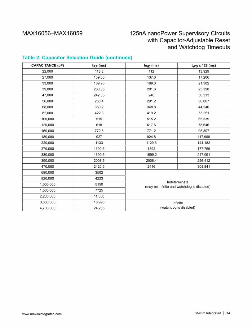
Table 2. Capacitor Selection Guide (continued)CAPACITANCE (pF) tRP (ms) tWD (ms) tWD x 128 (ms)
22,000 113.3 112 13,929
27,000 139.05 137.6 17,206
33,000 169.95 169.6 21,302
39,000 200.85 201.6 25,398
47,000 242.05 240 30,313
56,000 288.4 291.2 36,867
68,000 350.2 348.8 44,240
82,000 422.3 419.2 53,251
100,000 515 515.2 65,539
120,000 618 617.6 78,646
150,000 772.5 771.2 98,307
180,000 927 924.8 117,968
220,000 1133 1129.6 144,182
270,000 1390.5 1392 177,769
330,000 1699.5 1699.2 217,091
390,000 2008.5 2006.4 256,412
470,000 2420.5 2416 308,841
680,000 3502
Indeterminate(may be infinite and watchdog is disabled)
820,000 4223
1,000,000 5150
1,500,000 7725
2,200,000 11,330
3,300,000 16,995 Infinite(watchdog is disabled)4,700,000 24,205
MAX16056–MAX16059 125nA nanoPower Supervisory Circuits with Capacitor-Adjustable Reset
and Watchdog Timeouts
www.maximintegrated.com Maxim Integrated 14
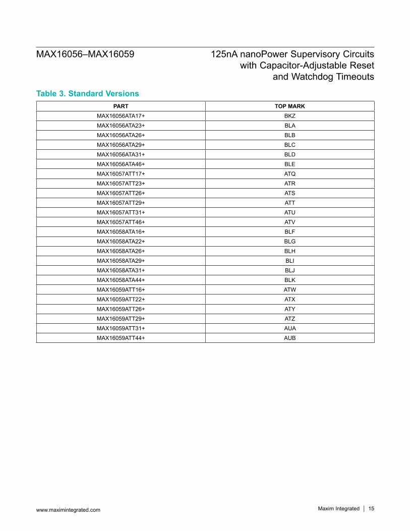
Table 3. Standard VersionsPART TOP MARK
MAX16056ATA17+ BKZ
MAX16056ATA23+ BLA
MAX16056ATA26+ BLB
MAX16056ATA29+ BLC
MAX16056ATA31+ BLD
MAX16056ATA46+ BLE
MAX16057ATT17+ ATQ
MAX16057ATT23+ ATR
MAX16057ATT26+ ATS
MAX16057ATT29+ ATT
MAX16057ATT31+ ATU
MAX16057ATT46+ ATV
MAX16058ATA16+ BLF
MAX16058ATA22+ BLG
MAX16058ATA26+ BLH
MAX16058ATA29+ BLI
MAX16058ATA31+ BLJ
MAX16058ATA44+ BLK
MAX16059ATT16+ ATW
MAX16059ATT22+ ATX
MAX16059ATT26+ ATY
MAX16059ATT29+ ATZ
MAX16059ATT31+ AUA
MAX16059ATT44+ AUB
MAX16056–MAX16059 125nA nanoPower Supervisory Circuits with Capacitor-Adjustable Reset
and Watchdog Timeouts
www.maximintegrated.com Maxim Integrated 15
Note: All devices are specified over the -40°C to +125°C oper-ating temperature range.+Denotes a lead(Pb)-free/RoHS-compliant package.T = Tape and reel.*EP = Exposed pad.“_ _” represents the two number suffix needed when ordering the reset threshold voltage value (see Table 1).Standard versions and their package top marks are shown in Table 3 at the end of data sheet.
Package InformationFor the latest package outline information and land patterns (footprints), go to www.maximintegrated.com/packages. Note that a “+”, “#”, or “-” in the package code indicates RoHS status only. Package drawings may show a different suffix character, but the drawing pertains to the package regardless of RoHS status.
Chip InformationPROCESS: BiCMOS
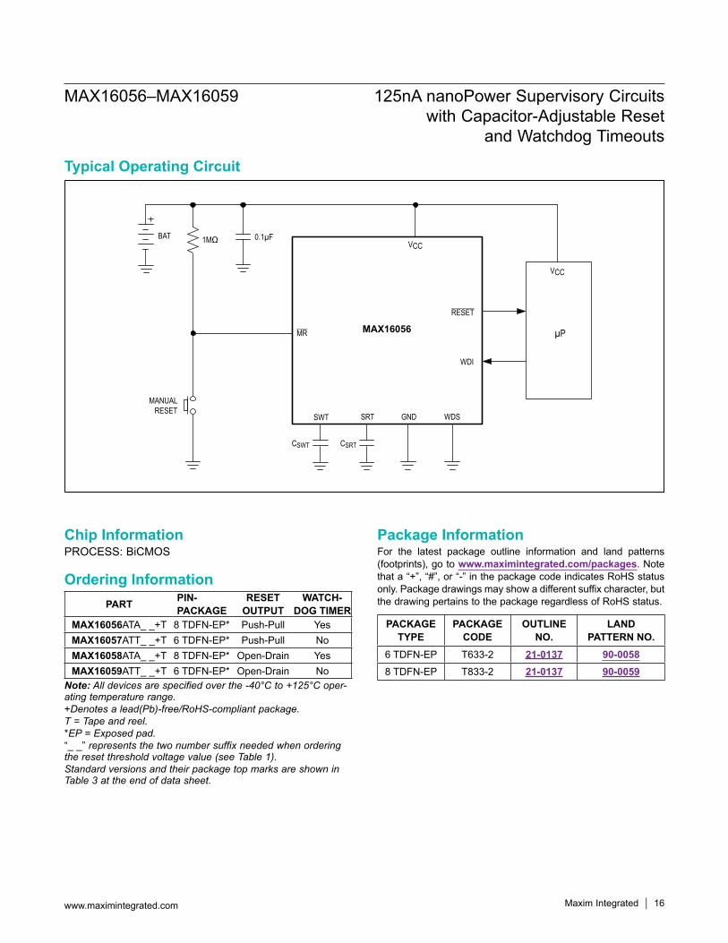
Typical Operating Circuit
PART PIN-PACKAGE
RESET OUTPUT
WATCH-DOG TIMER
MAX16056ATA_ _+T 8 TDFN-EP* Push-Pull YesMAX16057ATT_ _+T 6 TDFN-EP* Push-Pull NoMAX16058ATA_ _+T 8 TDFN-EP* Open-Drain YesMAX16059ATT_ _+T 6 TDFN-EP* Open-Drain No
Ordering Information
PACKAGE TYPE
PACKAGE CODE
OUTLINE NO.
LAND PATTERN NO.
6 TDFN-EP T633-2 21-0137 90-00588 TDFN-EP T833-2 21-0137 90-0059
MR
SWT SRT GND WDS
WDI
BAT 0.1µF
µP
MANUALRESET
1MΩ
CSWT CSRT
MAX16056RESET
VCC
VCC
MAX16056–MAX16059 125nA nanoPower Supervisory Circuits with Capacitor-Adjustable Reset
and Watchdog Timeouts
www.maximintegrated.com Maxim Integrated 16
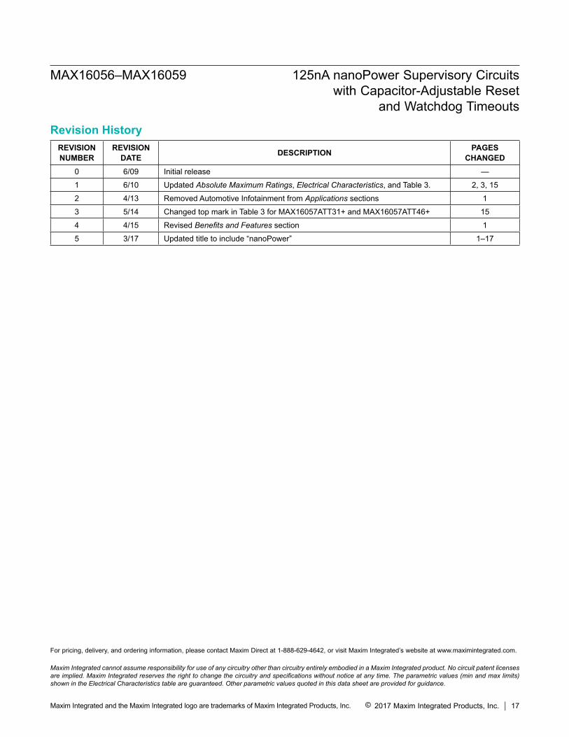
Revision HistoryREVISIONNUMBER
REVISIONDATE DESCRIPTION PAGES
CHANGED0 6/09 Initial release —
1 6/10 Updated Absolute Maximum Ratings, Electrical Characteristics, and Table 3. 2, 3, 15
2 4/13 Removed Automotive Infotainment from Applications sections 1
3 5/14 Changed top mark in Table 3 for MAX16057ATT31+ and MAX16057ATT46+ 15
4 4/15 Revised Benefits and Features section 1
5 3/17 Updated title to include “nanoPower” 1–17
Maxim Integrated cannot assume responsibility for use of any circuitry other than circuitry entirely embodied in a Maxim Integrated product. No circuit patent licenses are implied. Maxim Integrated reserves the right to change the circuitry and specifications without notice at any time. The parametric values (min and max limits) shown in the Electrical Characteristics table are guaranteed. Other parametric values quoted in this data sheet are provided for guidance.
Maxim Integrated and the Maxim Integrated logo are trademarks of Maxim Integrated Products, Inc.
MAX16056–MAX16059 125nA nanoPower Supervisory Circuits with Capacitor-Adjustable Reset
and Watchdog Timeouts
© 2017 Maxim Integrated Products, Inc. 17
For pricing, delivery, and ordering information, please contact Maxim Direct at 1-888-629-4642, or visit Maxim Integrated’s website at www.maximintegrated.com.