A product Line of Diodes Incorporated · PDF filePI5A100 December 2017 Diodes Incorporated ......
13
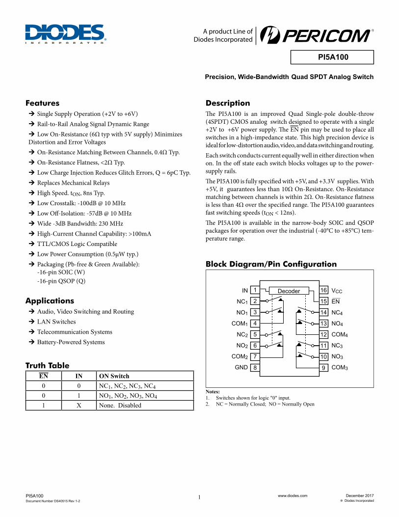
1 www.diodes.com December 2017 Diodes Incorporated PI5A100 Document Number DS40515 Rev 1-2 Block Diagram/Pin Configuration Features ¼ Single Supply Operation (+2V to +6V) ¼ Rail-to-Rail Analog Signal Dynamic Range ¼ Low On-Resistance (6Ω typ with 5V supply) Minimizes Distortion and Error Voltages ¼ On-Resistance Matching Between Channels, 0.4Ω Typ. ¼ On-Resistance Flatness, <2Ω Typ. ¼ Low Charge Injection Reduces Glitch Errors, Q = 6pC Typ. ¼ Replaces Mechanical Relays ¼ High Speed. t ON , 8ns Typ. ¼ Low Crosstalk: -100dB @ 10 MHz ¼ Low Off-Isolation: -57dB @ 10 MHz ¼ Wide -3dB Bandwidth: 230 MHz ¼ High-Current Channel Capability: >100mA ¼ TTL/CMOS Logic Compatible ¼ Low Power Consumption (0.5µW typ.) ¼ Packaging (Pb-free & Green Available): -16-pin SOIC (W) -16-pin QSOP (Q) Truth Table EN IN ON Switch 0 0 NC 1 , NC 2 , NC 3 , NC 4 0 1 NO 1 , NO 2 , NO 3 , NO 4 1 X None. Disabled Notes: 1. Switches shown for logic "0" input. 2. NC = Normally Closed; NO = Normally Open Description e PI5A100 is an improved Quad Single-pole double-throw (4SPDT) CMOS analog switch designed to operate with a single +2V to +6V power supply. e EN pin may be used to place all switches in a high-impedance state. is high precision device is ideal for low-distortion audio, video, and data switching and routing. Each switch conducts current equally well in either direction when on. In the off state each switch blocks voltages up to the power- supply rails. e PI5A100 is fully specified with +5V, and +3.3V supplies. With +5V, it guarantees less than 10Ω On-Resistance. On-Resistance matching between channels is within 2Ω. On-Resistance flatness is less than 4Ω over the specified range. e PI5A100 guarantees fast switching speeds (t ON < 12ns). e PI5A100 is available in the narrow-body SOIC and QSOP packages for operation over the industrial (-40°C to +85°C) tem- perature range. 1 2 3 4 5 6 7 8 16 15 14 13 12 11 10 9 VCC EN NC4 NO 4 COM 4 NC 3 NO 3 COM 3 IN NC1 NO 1 COM 1 NC 2 NO 2 COM 2 GND Decoder Precision, Wide-Bandwidth Quad SPDT Analog Switch A product Line of Diodes Incorporated PI5A100 Applications ¼ Audio, Video Switching and Routing ¼ LAN Switches ¼ Telecommunication Systems ¼ Battery-Powered Systems
Transcript of A product Line of Diodes Incorporated · PDF filePI5A100 December 2017 Diodes Incorporated ......
1 www.diodes.com December 2017 Diodes Incorporated
PI5A100 Document Number DS40515 Rev 1-2
Block Diagram/Pin Configuration
Features ¼ Single Supply Operation (+2V to +6V) ¼ Rail-to-Rail Analog Signal Dynamic Range ¼ Low On-Resistance (6Ω typ with 5V supply) Minimizes
Distortion and Error Voltages ¼ On-Resistance Matching Between Channels, 0.4Ω Typ. ¼ On-Resistance Flatness, <2Ω Typ. ¼ Low Charge Injection Reduces Glitch Errors, Q = 6pC Typ. ¼ Replaces Mechanical Relays ¼ High Speed. tON, 8ns Typ. ¼ Low Crosstalk: -100dB @ 10 MHz ¼ Low Off-Isolation: -57dB @ 10 MHz ¼ Wide -3dB Bandwidth: 230 MHz ¼ High-Current Channel Capability: >100mA ¼ TTL/CMOS Logic Compatible ¼ Low Power Consumption (0.5µW typ.) ¼ Packaging (Pb-free & Green Available):
-16-pin SOIC (W) -16-pin QSOP (Q)
Truth TableEN IN ON Switch0 0 NC1, NC2, NC3, NC4
0 1 NO1, NO2, NO3, NO4
1 X None. Disabled
Notes:1. Switches shown for logic "0" input.2. NC = Normally Closed; NO = Normally Open
DescriptionThe PI5A100 is an improved Quad Single-pole double-throw (4SPDT) CMOS analog switch designed to operate with a single +2V to +6V power supply. The EN pin may be used to place all switches in a high-impedance state. This high precision device is ideal for low-distortion audio, video, and data switching and routing. Each switch conducts current equally well in either direction when on. In the off state each switch blocks voltages up to the power-supply rails.The PI5A100 is fully specified with +5V, and +3.3V supplies. With +5V, it guarantees less than 10Ω On-Resistance. On-Resistance matching between channels is within 2Ω. On-Resistance flatness is less than 4Ω over the specified range. The PI5A100 guarantees fast switching speeds (tON < 12ns). The PI5A100 is available in the narrow-body SOIC and QSOP packages for operation over the industrial (-40°C to +85°C) tem-perature range.
1
2
3
4
5
6
7
8
16
15
14
13
12
11
10
9
VCC
EN
NC4
NO4
COM4
NC3
NO3
COM3
IN
NC1
NO1
COM1
NC2
NO2
COM2
GND
Decoder
Precision, Wide-Bandwidth Quad SPDT Analog Switch
A product Line ofDiodes Incorporated
PI5A100
Applications ¼ Audio, Video Switching and Routing ¼ LAN Switches ¼ Telecommunication Systems ¼ Battery-Powered Systems
2
A product Line ofDiodes Incorporated
PI5A100
www.diodes.com December 2017 Diodes Incorporated
PI5A100 Document Number DS40515 Rev 1-2
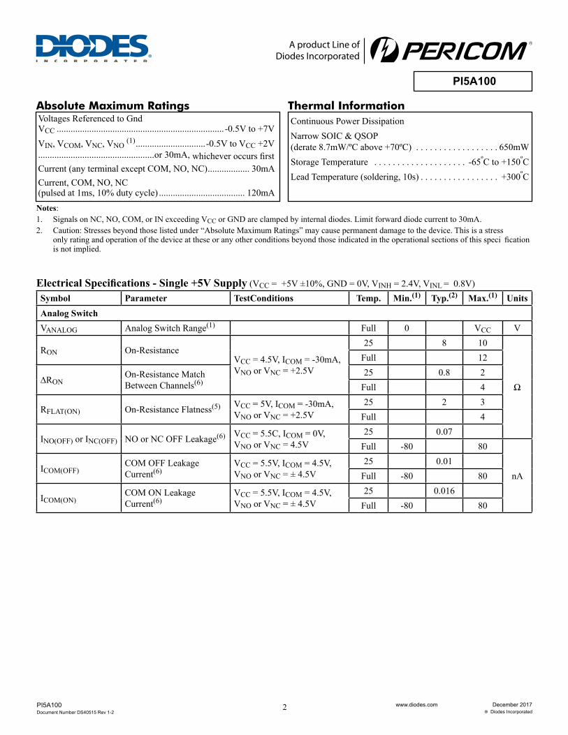
Absolute Maximum RatingsContinuous Power DissipationNarrow SOIC & QSOP (derate 8.7mW/ºC above +70ºC) . . . . . . . . . . . . . . . . . . 650mWStorage Temperature . . . . . . . . . . . . . . . . . . . . -65ºC to +150ºCLead Temperature (soldering, 10s) . . . . . . . . . . . . . . . . . +300ºC
Voltages Referenced to Gnd VCC ........................................................................ -0.5V to +7VVIN, VCOM, VNC, VNO (1) ..............................-0.5V to VCC +2V ..................................................or 30mA, whichever occurs firstCurrent (any terminal except COM, NO, NC) .................. 30mACurrent, COM, NO, NC (pulsed at 1ms, 10% duty cycle) ..................................... 120mANotes:1. Signals on NC, NO, COM, or IN exceeding VCC o r GND are clamped by internal diodes. Limit forward diode current to 30mA.2. Caution: Stresses beyond those listed under “Absolute Maximum Ratings” may cause permanent damage to the device. This is a stress
only rating and operation of the device at these or any other conditions beyond those indicated in the operational sections of this speci fication is not implied.
Electrical Specifications - Single +5V Supply (VCC = +5V ±10%, GND = 0V, VINH = 2.4V, VINL = 0.8V)Symbol Parameter TestConditions Temp. Min.(1) Typ.(2) Max.(1) UnitsAnalog SwitchVANALOG Analog Switch Range(1) Full 0 VCC V
RON On-ResistanceVCC = 4.5V, ICOM = -30mA,VNO or VNC = +2.5V
25 8 10
Ω
Full 12
∆RONOn-Resistance Match Between Channels(6)
25 0.8 2Full 4
RFLAT(ON) On-Resistance Flatness(5) VCC = 5V, ICOM = -30mA, VNO or VNC = +2.5V
25 2 3Full 4
INO(OFF) or INC(OFF) NO or NC OFF Leakage(6) VCC = 5.5C, ICOM = 0V, VNO or VNC = 4.5V
25 0.07Full -80 80
nAICOM(OFF)
COM OFF LeakageCurrent(6)
VCC = 5.5V, ICOM = 4.5V, VNO or VNC = ± 4.5V
25 0.01Full -80 80
ICOM(ON)COM ON LeakageCurrent(6)
VCC = 5.5V, ICOM = 4.5V, VNO or VNC = ± 4.5V
25 0.016Full -80 80
Thermal Information
3
A product Line ofDiodes Incorporated
PI5A100
www.diodes.com December 2017 Diodes Incorporated
PI5A100 Document Number DS40515 Rev 1-2
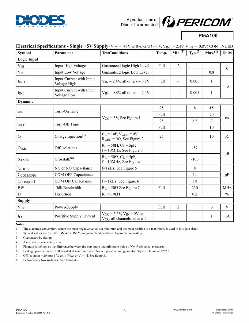
Notes:1. The algebraic convention, where the most negative value is a minimum and the most positive is a maximum, is used in this data sheet. 2. Typical values are for DESIGN AID ONLY, not guaranteed or subject to production testing.3. Guaranteed by design4. ΔRΟΝ = RΟΝ max - RΟΝ min5. Flatness is defined as the difference between the maximum and minimum value of On-Resistance measured. 6. Leakage parameters are 100% tested at maximum rated hot temperature and guaranteed by correlation at +25ºC.7. Off Isolation = 20log10 [ VCOM / (VNO or VNC) ]. See figure 3.8. Between any two switches. See figure 4.-
Electrical Specifications - Single +5V Supply (VCC = +5V ±10%, GND = 0V, VINH = 2.4V, VINL = 0.8V) CONTINUEDSymbol Parameter TestConditions Temp. Min.(1) Typ.(2) Max.(1) UnitsLogic InputVIH Input High Voltage Guaranteed logic High Level Full 2
VVIL Input Low Voltage Guaranteed logic Low Level 0.8
IINHInput Current with Input Voltage High VIN = 2.4V, all others = 0.8V Full -1 0.005 1
µAIINL
Input Current with Input Voltage Low VIN = 0.8V, all others = 2.4V -1 0.005 1
Dynamic
tON Turn-On TimeVCC = 5V, See Figure 1
25 8 15
nsFull 20
tOFF Turn-Off Time25 3.5 7
Full 10
Q Charge Injection(3) CL = 1nF, VGEN = 0V, RGEN = 0Ω, See Figure 2 25 10 pC
OIRR Off Isolations RL = 50Ω, CL = 5pF, f = 10MHz, See Figure 3 -57
dBXTALK Crosstalk(8) RL = 50Ω, CL = 5pF,
f = 10MHz, See Figure 4 -100
C(OFF) NC or NO Capacitance f=1kHz, See Figure 5 8pFCCOM(OFF) COM OFF Capacitance 14
CCOM(ON) COM ON Capacitance f = 1kHz, See Figure 6 18BW -3db Bandwidth RL = 50Ω See Figure 7 Full 230 MHzD Distortion RL = 10kΩ 0.2 %SupplyVCC Power-Supply Full 2 6 V
ICC Postitive Supply Current VCC = 5.5V, VIN = 0V or VCC, all channels on or off 1 µA
4
A product Line ofDiodes Incorporated
PI5A100
www.diodes.com December 2017 Diodes Incorporated
PI5A100 Document Number DS40515 Rev 1-2
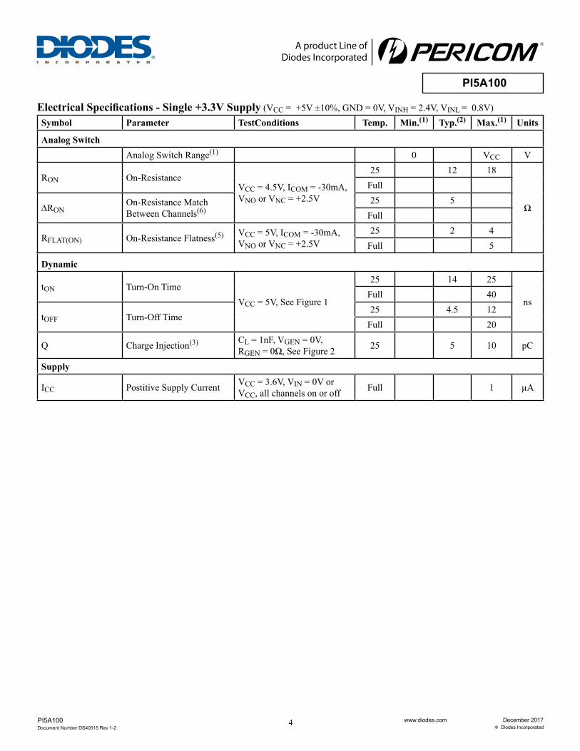
Electrical Specifications - Single +3.3V Supply (VCC = +5V ±10%, GND = 0V, VINH = 2.4V, VINL = 0.8V)Symbol Parameter TestConditions Temp. Min.(1) Typ.(2) Max.(1) Units
Analog SwitchAnalog Switch Range(1) 0 VCC V
RON On-ResistanceVCC = 4.5V, ICOM = -30mA,VNO or VNC = +2.5V
25 12 18
Ω
Full
∆RONOn-Resistance Match Between Channels(6)
25 5Full
RFLAT(ON) On-Resistance Flatness(5) VCC = 5V, ICOM = -30mA, VNO or VNC = +2.5V
25 2 4Full 5
Dynamic
tON Turn-On TimeVCC = 5V, See Figure 1
25 14 25
nsFull 40
tOFF Turn-Off Time25 4.5 12
Full 20
Q Charge Injection(3) CL = 1nF, VGEN = 0V, RGEN = 0Ω, See Figure 2 25 5 10 pC
Supply
ICC Postitive Supply Current VCC = 3.6V, VIN = 0V or VCC, all channels on or off Full 1 µA
5
A product Line ofDiodes Incorporated
PI5A100
www.diodes.com December 2017 Diodes Incorporated
PI5A100 Document Number DS40515 Rev 1-2
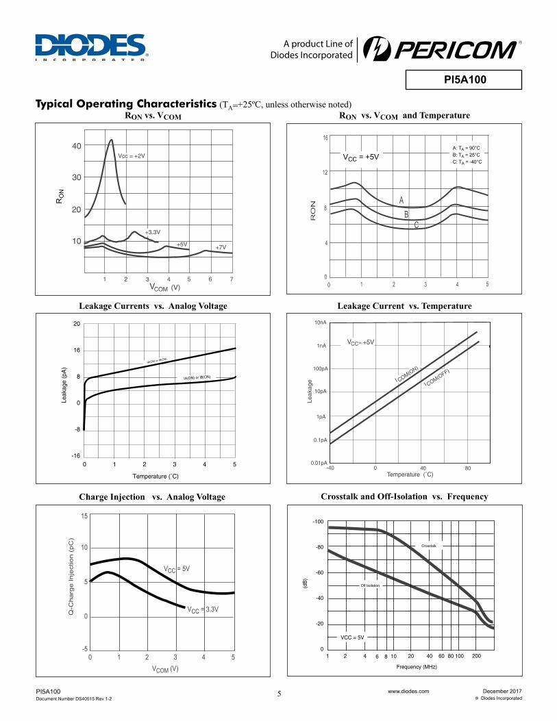
Typical Operating Characteristics (Ta=+25ºC, unless otherwise noted)
Charge Injection vs. Analog Voltage
Leakage Current vs. Temperature
Crosstalk and Off-Isolation vs. Frequency
RON vs. VCOM RON vs. VCOM and Temperature
Leakage Currents vs. Analog Voltage
20
V
10
30
40
+5V +7V
COM
1 2 3 4 5 6 7
(V)
Vcc = +2V
+3.3V
RO
N
8
4
12
16
1 2 3 4 5
RO
N
0
AB
C
0
VCC = +5VA: TA = 90°CB: TA = 25°CC: TA = -40°C
-40 40 80
10nA
1nA
100pA
10pA
1pA
0.1pA
0.01pA
Temperature (˚C)
Leak
age
II
0
COM(ON)
COM(OFF)
CC= +5VV
20
16
8
0
-8
-160 1 2 3 4 5
Temperature (˚C)
Leak
age
(pA
)
IA(ON) or IB(ON)
IA(ON) or IB(ON)
15
10
5
0
-50 1 2 3 4 5
Q-C
harg
e Inje
ctio
n (
pC
)
VCC = 3.3V
VCC = 5V
VCOM (V)
-100
-80
-60
-40
-20
01 2 4 6 8 10 20 40 60 80 100 200
Off Isolation
Crosstalk
VCC = 5V
Frequency (MHz)
(dB
)
6
A product Line ofDiodes Incorporated
PI5A100
www.diodes.com December 2017 Diodes Incorporated
PI5A100 Document Number DS40515 Rev 1-2
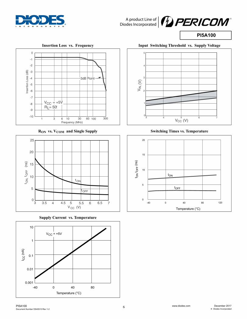
RON vs. VCOM and Single Supply Switching Times vs. Temperature
Insertion Loss vs. Frequency Input Switching Threshold vs. Supply Voltage
Supply Current vs. Temperature
10
1
0.1
0.01
0.001-40 0 40 80
Temperature (°C)
VCC = +5V
I CC
(nA
)
0
-1
-2
-3
-4
-5
-6
-7
-8
-9
-1031 6 10 30 60 100 300
Inse
rtio
n Lo
ss (
dB)
Frequency (MHz)
R = 50!
-3dB Point
L
V = +5VCC
4
3
2
1
0
5
43 75 6
VIN
, (V
)
VCC (V)
4.5 75 5.5 6.5643.5
20
15
10
5
0
25
3
t ON
,t O
FF
(ns)
V CC (V)
tON,
tOFF
-400
5
10
15
20
0 40 80 120
Temperature (°C)
t ON
t OFF
(ns)
tON
tOFF
7
A product Line ofDiodes Incorporated
PI5A100
www.diodes.com December 2017 Diodes Incorporated
PI5A100 Document Number DS40515 Rev 1-2
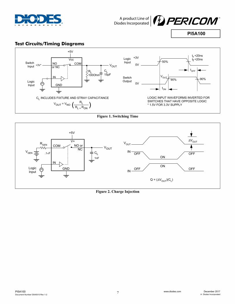
Test Circuits/Timing Diagrams
Figure 1. Switching Time
Figure 2. Charge Injection
Vcc
+5V
NO
GND
or NCCOM +3V*
LogicInput
IN
tr <20nstf <20ns
VOUT = VNORL
RL + RON( )
CL INCLUDES FIXTURE AND STRAY CAPACITANCE
VOUT
RL100Ohm
CL15pF
LOGIC INPUT WAVEFORMS INVERTED FOR SWITCHES THAT HAVE OPPOSITE LOGIC* 1.5V FOR 3.3V SUPPLY
tOFF
tON
VOUT90% 90%
LogicInput
SwitchOutput
+3V
0V
0V
50%SwitchInput
V+
+5V
NO or
GND
NCCOM VOUT
CL1nF
VOUT ∆VOUT
INVGEN
ON
ON
OFF
OFF
OFF
OFFIN
Q = (∆VOUT)(CL)
IN
LogicInput
.1∝F
RGEN
8
A product Line ofDiodes Incorporated
PI5A100
www.diodes.com December 2017 Diodes Incorporated
PI5A100 Document Number DS40515 Rev 1-2
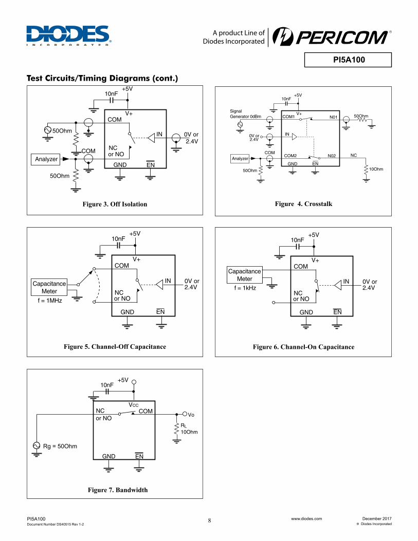
Test Circuits/Timing Diagrams (cont.)
Figure 3. Off Isolation
Figure 5. Channel-Off Capacitance
Figure 4. Crosstalk
Figure 6. Channel-On Capacitance
Figure 7. Bandwidth
V+
+5V
AnalyzerGND EN
N02
COM1
10nF
COM
SignalGenerator 0dBm
0V or2.4V
COM2
IN
N01
NC
50Ohm
10Ohm50Ohm
V+
+5V
NC
CapacitanceMeter
GND EN
or NO
COM
10nF
IN 0V or2.4V
f = 1MHz
V+
+5V
NC
CapacitanceMeter
GND EN
or NO
COM
10nF
IN 0V or2.4Vf = 1kHz
V+
+5V
NC
AnalyzerGND EN
or NO
COM
10nF
IN
COM
50Ohm
50Ohm0V or 2.4V
VCC
+5V
NC
GND EN
or NO
10nF
Rg = 50Ohm
COM
RL
10Ohm
Vo
9
A product Line ofDiodes Incorporated
PI5A100
www.diodes.com December 2017 Diodes Incorporated
PI5A100 Document Number DS40515 Rev 1-2
Applications Information
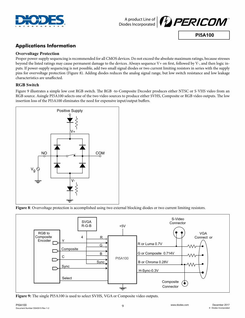
Overvoltage Protection Proper power-supply sequencing is recommended for all CMOS devices. Do not exceed the absolute maximum ratings, because stresses beyond the listed ratings may cause permanent damage to the devices. Always sequence V+ on first, followed by V-, and then logic in-puts. If power-supply sequencing is not possible, add two small signal diodes or two current limiting resistors in series with the supply pins for overvoltage protection (Figure 8). Adding diodes reduces the analog signal range, but low switch resistance and low leakage characteristics are unaffected.
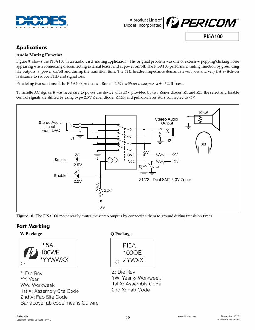
RGB SwitchFigure 9 illustrates a simple low cost RGB switch. The RGB -to-Composite Decoder produces either NTSC or S-VHS video from an RGB source. Asingle PI5A100 selects one of the two video sources to produce either SVHS, Composite or RGB video outputs. The low insertion loss of the PI5A100 eliminates the need for expensive input/output buffers.
Figure 8: Overvoltage protection is accomplished using two external blocking diodes or two current limiting resistors.
Figure 9: The single PI5A100 is used to select SVHS, VGA or Composite video outputs.
V+
Positive Supply
COMNO
Vg
V-
Select
C
CompositeConnector
S-VideoConnector
Composite
RGB to Composite
Encoder
SVGAR-G-B
Sync
R
B
+5V
G
Sync
4Y
PI5A100
H-Sync-0.3V
G or Composite 0.714V
R or Luma 0.7V
B or Chroma 0.28V
VGAConnect or
10
A product Line ofDiodes Incorporated
PI5A100
www.diodes.com December 2017 Diodes Incorporated
PI5A100 Document Number DS40515 Rev 1-2
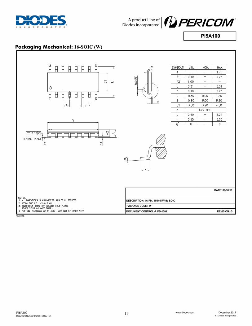
Applications Audio Muting FunctionFigure 8 shows the PI5A100 in an audio card muting application. The original problem was one of excessive popping/clicking noise appearing when connecting disconnecting external loads, and at power on/off. The PI5A100 performs a muting function by grounding the outputs at power on/off and during the transition time. The 32Ω headset impedance demands a very low and very flat switch-on resistance to reduce THD and signal loss.
Paralleling two sections of the PI5A100 produces a Ron of 2.5Ω with an unsurpassed ±0.5Ω flatness.
To handle AC signals it was necessary to power the device with ±3V provided by two Zener diodes: Z1 and Z2. The select and Enable control signals are shifted by using twpo 2.5V Zener diodes Z3,Z4 and pull down resistors connected to -3V.
Figure 10: The PI5A100 momentarily mutes the stereo outputs by connecting them to ground during transition times.
VccGND
Select
J2J1
Z1/Z2 - Dual SMT 3.0V Zener
32!
22k!
2.5V
-3V
Stereo Audio Output
2.5V
Z3
Z4Enable
Z1 Z2
+5V
-5V-3V
Stereo Audio Input
From DAC
10kW
Part Marking
PI5A100WE*YYWWXX
*: Die RevYY: YearWW: Workweek1st X: Assembly Site Code2nd X: Fab Site CodeBar above fab code means Cu wire
W Package
PI5A100QEZYWXX
Z: Die RevYW: Year & Workweek1st X: Assembly Code2nd X: Fab Code
Q Package
11
A product Line ofDiodes Incorporated
PI5A100
www.diodes.com December 2017 Diodes Incorporated
PI5A100 Document Number DS40515 Rev 1-2
Packaging Mechanical: 16-SOIC (W)
16-0145
12
A product Line ofDiodes Incorporated
PI5A100
www.diodes.com December 2017 Diodes Incorporated
PI5A100 Document Number DS40515 Rev 1-2
Ordering InformationOrdering Code Package Code Package DescriptionPI5A100WEX W 16-pin, 150mil Wide (SOIC)PI5A100QEX Q 16-pin, 150mil Wide (QSOP)
Packaging Mechanical: 16-QSOP (Q)
16-0056
Notes:
• Thermal characteristics can be found on the company web site at www.diodes.com/design/support/packaging/• E = Pb-free and Green• X suffix = Tape/Reel
For latest package info. please check: http://www.diodes.com/design/support/packaging/pericom-packaging/packaging-mechanicals-and-thermal-characteristics/
13
A product Line ofDiodes Incorporated
PI5A100
www.diodes.com December 2017 Diodes Incorporated
PI5A100 Document Number DS40515 Rev 1-2
IMPORTANT NOTICE
DIODES INCORPORATED MAKES NO WARRANTY OF ANY KIND, EXPRESS OR IMPLIED, WITH REGARDS TO THIS DOCUMENT, INCLUDING, BUT NOT LIMITED TO, THE IMPLIED WARRANTIES OF MERCHANTABILITY AND FITNESS FOR A PARTICULAR PURPOSE (AND THEIR EQUIVALENTS UNDER THE LAWS OF ANY JURISDICTION). Diodes Incorporated and its subsidiaries reserve the right to make modifications, enhancements, improvements, corrections or other changes without further notice to this document and any product described herein. Diodes Incorporated does not assume any liability arising out of the application or use of this document or any product described herein; neither does Diodes Incorporated convey any license under its patent or trademark rights, nor the rights of others. Any Customer or user of this document or products described herein in such applications shall assume all risks of such use and will agree to hold Diodes Incorporated and all the companies whose products are represented on Diodes Incorporated website, harmless against all damages. Diodes Incorporated does not warrant or accept any liability whatsoever in respect of any products purchased through unauthorized sales channel.Should Customers purchase or use Diodes Incorporated products for any unintended or unauthorized application, Customers shall indemnify and hold Diodes Incor-porated and its representatives harmless against all claims, damages, expenses, and attorney fees arising out of, directly or indirectly, any claim of personal injury or death associated with such unintended or unauthorized application.Products described herein may be covered by one or more United States, international or foreign patents pending. Product names and markings noted herein may also be covered by one or more United States, international or foreign trademarks.
This document is written in English but may be translated into multiple languages for reference. Only the English version of this document is the final and determina-tive format released by Diodes Incorporated.
LIFE SUPPORTDiodes Incorporated products are specifically not authorized for use as critical components in life support devices or systems without the express written approval of the Chief Executive Officer of Diodes Incorporated. As used herein:A. Life support devices or systems are devices or systems which: 1. are intended to implant into the body, or2. support or sustain life and whose failure to perform when properly used in accordance with instructions for use provided in the labeling can be reasonably expected to result in significant injury to the user.B. A critical component is any component in a life support device or system whose failure to perform can be reasonably expected to cause the failure of the life support device or to affect its safety or effectiveness.Customers represent that they have all necessary expertise in the safety and regulatory ramifications of their life support devices or systems, and acknowledge and agree that they are solely responsible for all legal, regulatory and safety-related requirements concerning their products and any use of Diodes Incorporated products in such safety-critical, life support devices or systems, notwithstanding any devices- or systems-related information or support that may be provided by Diodes Incor-porated. Further, Customers must fully indemnify Diodes Incorporated and its representatives against any damages arising out of the use of Diodes Incorporated products in such safety-critical, life support devices or systems.
Copyright © 2016, Diodes Incorporatedwww.diodes.com