Pb A product Line of Diodes Incorporated Lead-free Green ...
11
1 www.diodes.com August 2019 Diodes Incorporated PI3USB223 Document Number DS42160 Rev 1-3 Features ¼ Single +2.7V to +4.4V Supply Voltage ¼ Low 50µA Supply Current ¼ -3dB Bandwidth: 1500MHz (typ) ¼ Low 2.5Ω(typ)On-Resistance ¼ THD+N: 0.02% ¼ Shorting D+/R and D-/L to Vbus will not cause leakage when V DD = 0 ¼ Internal Shunt Resistors for Click-and-Pop Reduction ¼ VBUS Detection for Automatic Switch Path Selection ¼ Totally Lead-Free & Fully RoHS Compliant (Notes 1 & 2) ¼ Halogen and Antimony Free. “Green” Device (Note 3) ¼ Packaging (Pb-free & Green available): • 10-pin contact UQFN, 1.4 x 1.8, (ZM10) Description e PI3USB223 combines AC coupled audio signals and USB2.0 HS (480Mbps) on the same pins. is enables users to use a single connector to drive either a USB end point or an audio end point. PI3USB223 incorporates gate pump technology required to maintain low Ron for ideal audio THD while reducing the capacitance affect of high speed USB signals. e device also incorporates a substrate pump technology which allows -2V signals to pass through the switch without causing any leakage. e PI3USB223 features protection on D+/R and D-/L to ensure no damage will happen to the IC if these pins are shorted accidentally to Vbus as well as ensuring there is no leakage when V DD is on or off. Also, it includes VBUS detection (VB) to automatically switch to the USB signal path upon detection of a valid VBUS signal. It also features internal shunt resistors on the audio path to reduce clicks and pops heard during output. e device is available in a space-saving 10-pin, 1.4mm x 1.8mm UQFN package, and operate over the -40°C to +85°C temperature range. Block Diagram Truth Table ASEL V DD VBUS L/R D+/D- L/R Shunt X L L OFF OFF OFF X H L OFF OFF ON X L H OFF OFF OFF L H H OFF ON ON H H H ON OFF OFF VVBDET VBUS D+/R D-/L D+ D- R L ASEL A product Line of Diodes Incorporated PI3USB223 USB 2.0 High-Speed and Audio Switches with Negative Signal Capability Notes: 1. No purposely added lead. Fully EU Directive 2002/95/EC (RoHS), 2011/65/EU (RoHS 2) & 2015/863/EU (RoHS 3) compliant. 2. See https://www.diodes.com/quality/lead-free/ for more information about Diodes Incorporated’s definitions of Halogen- and Antimony-free, "Green" and Lead-free. 3. Halogen- and Antimony-free "Green” products are defined as those which contain <900ppm bromine, <900ppm chlorine (<1500ppm total Br + Cl) and <1000ppm antimony compounds. b P Lead-free Green
Transcript of Pb A product Line of Diodes Incorporated Lead-free Green ...
1www.diodes.com August 2019
Diodes IncorporatedPI3USB223 Document Number DS42160 Rev 1-3
Features ¼Single +2.7V to +4.4V Supply Voltage ¼Low 50µA Supply Current ¼ -3dB Bandwidth: 1500MHz (typ) ¼Low 2.5Ω(typ)On-Resistance ¼THD+N: 0.02% ¼Shorting D+/R and D-/L to Vbus will not cause leakage when VDD = 0
¼ Internal Shunt Resistors for Click-and-Pop Reduction ¼VBUS Detection for Automatic Switch Path Selection ¼Totally Lead-Free & Fully RoHS Compliant (Notes 1 & 2) ¼Halogen and Antimony Free. “Green” Device (Note 3) ¼Packaging (Pb-free & Green available):• 10-pin contact UQFN, 1.4 x 1.8, (ZM10)
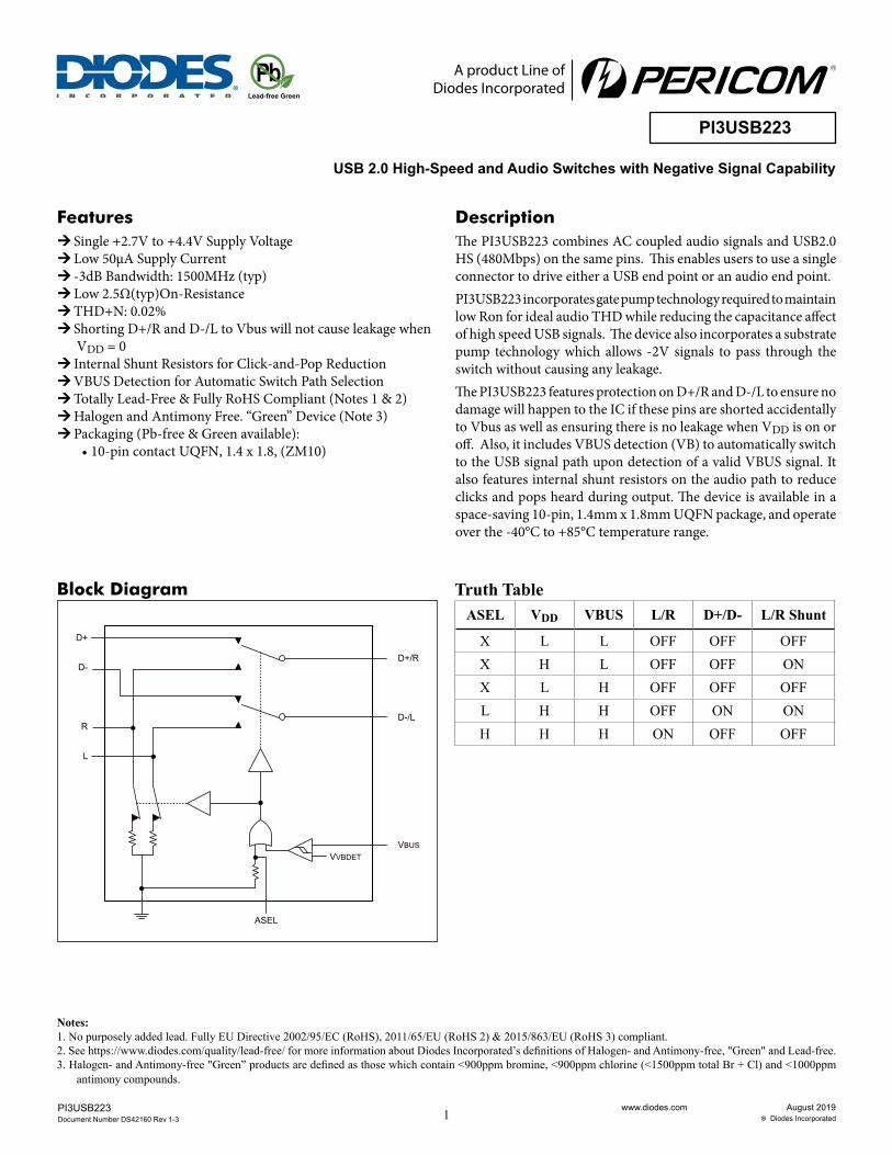
DescriptionThe PI3USB223 combines AC coupled audio signals and USB2.0 HS (480Mbps) on the same pins. This enables users to use a single connector to drive either a USB end point or an audio end point.PI3USB223 incorporates gate pump technology required to maintain low Ron for ideal audio THD while reducing the capacitance affect of high speed USB signals. The device also incorporates a substrate pump technology which allows -2V signals to pass through the switch without causing any leakage.The PI3USB223 features protection on D+/R and D-/L to ensure no damage will happen to the IC if these pins are shorted accidentally to Vbus as well as ensuring there is no leakage when VDD is on or off. Also, it includes VBUS detection (VB) to automatically switch to the USB signal path upon detection of a valid VBUS signal. It also features internal shunt resistors on the audio path to reduce clicks and pops heard during output. The device is available in a space-saving 10-pin, 1.4mm x 1.8mm UQFN package, and operate over the -40°C to +85°C temperature range.
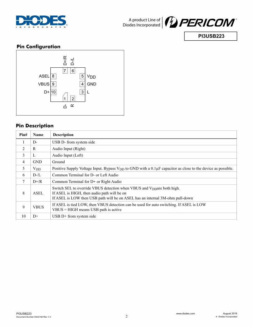
Block Diagram Truth TableASEL VDD VBUS L/R D+/D- L/R Shunt
X L L OFF OFF OFFX H L OFF OFF ONX L H OFF OFF OFFL H H OFF ON ONH H H ON OFF OFF
VVBDETVBUS
D+/R
D-/L
D+
D-
R
L
ASEL
A product Line ofDiodes Incorporated
PI3USB223
USB 2.0 High-Speed and Audio Switches with Negative Signal Capability
Notes: 1. No purposely added lead. Fully EU Directive 2002/95/EC (RoHS), 2011/65/EU (RoHS 2) & 2015/863/EU (RoHS 3) compliant. 2. See https://www.diodes.com/quality/lead-free/ for more information about Diodes Incorporated’s definitions of Halogen- and Antimony-free, "Green" and Lead-free. 3. Halogen- and Antimony-free "Green” products are defined as those which contain <900ppm bromine, <900ppm chlorine (<1500ppm total Br + Cl) and <1000ppm
antimony compounds.
bPLead-free Green
Sherry_Wang838
矩形
Sherry_Wang838
打字機文字
Obsolete – Part Discontinued
2
A product Line ofDiodes Incorporated
PI3USB223
www.diodes.com August 2019 Diodes Incorporated
PI3USB223 Document Number DS42160 Rev 1-3
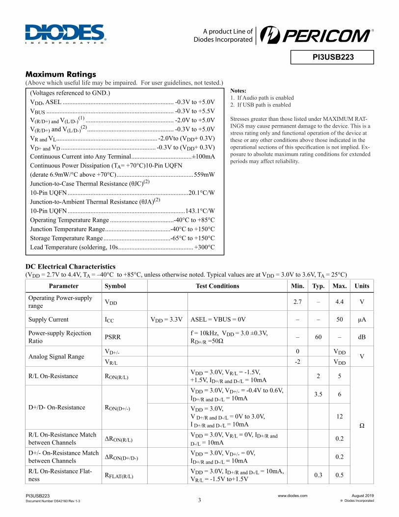
Pin Description
Pin# Name Description
1 D- USB D- from system side2 R Audio Input (Right)3 L Audio Input (Left)4 GND Ground5 VDD Positive Supply Voltage Input. Bypass VDD to GND with a 0.1µF capacitor as close to the device as possible.6 D-/L Common Terminal for D- or Left Audio7 D+/R Common Terminal for D+ or Right Audio
8 ASELSwitch SEL to override VBUS detection when VBUS and VDDare both high. If ASEL is HIGH, then audio path will be onIf ASEL is LOW then USB path will be on ASEL has an internal 3M-ohm pull-down
9 VBUS If ASEL is tied LOW, then VBUS detection can be used for auto switching. If ASEL is LOWVBUS = HIGH means USB path is active
10 D+ USB D+ from system side
Pin Configuration
8
9
10
5
4
3
VDD
GND
L
ASEL
VBUS
D+
7 6
1 2
D- R
D+/
R
D-/L
8
9
10
3
A product Line ofDiodes Incorporated
PI3USB223
www.diodes.com August 2019 Diodes Incorporated
PI3USB223 Document Number DS42160 Rev 1-3
DC Electrical Characteristics (VDD = 2.7V to 4.4V, TA = –40°C to +85°C, unless otherwise noted. Typical values are at VDD = 3.0V to 3.6V, TA = 25°C)
Parameter Symbol Test Conditions Min. Typ. Max. Units
Operating Power-supply range VDD 2.7 – 4.4 V
Supply Current ICC VDD = 3.3V ASEL = VBUS = 0V – – 50 μA
Power-supply Rejection Ratio PSRR f = 10kHz, VDD = 3.0 ±0.3V,
RD+/R =50Ω – 60 – dB
Analog Signal RangeVD+/- 0 VDD VVR/L -2 VDD
R/L On-Resistance RON(R/L)VDD = 3.0V, VR/L = -1.5V, +1.5V, ID+/R and D-/L = 10mA 2 5
Ω
D+/D- On-Resistance RON(D+/-)
VDD = 3.0V, VD+/- = -0.4V to 0.6V, ID+/R and D-/L = 10mA 3.5 6
VDD = 3.0V, V D+/R and D-/L = 0V to 3.0V, I D+/R and D-/L = 10mA
12
R/L On-Resistance Match between Channels ΔRON(R/L)
VDD = 3.0V, VR/L = 0V, ID+/R and D-/L = 10mA 0.2
D+/- On-Resistance Match between Channels ΔRON(D+/D-)
VDD = 3.0V, VD+/- = 0V, ID+/R and D-/L = 10mA 0.2
R/L On-Resistance Flat-ness RFLAT(R/L)
VDD = 3.0V, ID+/R and D-/L = 10mA, VR/L = -1.5V to+1.5V 0.3 0.5
(Voltages referenced to GND.)VDD, ASEL .................................................................... -0.3V to +5.0VVBUS .............................................................................. -0.3V to +5.5VV(R/D+) and V(L/D-)
(1) ...................................................... -2.0V to +5.0VV(R/D+) and V(L/D-)
(2) ..................................................... -0.3V to +5.0VVR and VL .............................................................. -2.0Vto (VDD+ 0.3V)VD+ and VD .......................................................... -0.3V to (VDD+ 0.3V)Continuous Current into Any Terminal .....................................±100mAContinuous Power Dissipation (TA= +70°C)10-Pin UQFN (derate 6.9mW/°C above +70°C) ...............................................559mW Junction-to-Case Thermal Resistance (θJC)(2)
10-Pin UQFN ..........................................................................20.1°C/WJunction-to-Ambient Thermal Resistance (θJA)(2)
10-Pin UQFN ........................................................................143.1°C/WOperating Temperature Range .......................................-40°C to +85°CJunction Temperature Range ........................................-40°C to +150°CStorage Temperature Range .........................................-65°C to +150°CLead Temperature (soldering, 10s .............................................. +300°C
Notes: 1. If Audio path is enabled2. If USB path is enabled
Stresses greater than those listed under MAXIMUM RAT-INGS may cause permanent damage to the device. This is a stress rating only and functional operation of the device at these or any other conditions above those indicated in the operational sections of this specification is not implied. Ex-posure to absolute maximum rating conditions for extended periods may affect reliability.
Maximum Ratings(Above which useful life may be impaired. For user guidelines, not tested.)
4
A product Line ofDiodes Incorporated
PI3USB223
www.diodes.com August 2019 Diodes Incorporated
PI3USB223 Document Number DS42160 Rev 1-3
Parameter Symbol Test Conditions Min. Typ. Max. Units
D+/D- On-Resistance Flatness RFLAT(D+/-)
VDD = 3.0V, I D+/R and D-/L = 10m A, VD+/- = -0.4V to 0.6V 0.25 0.5 Ω
Shunt Switch Resistance RSH Voltage on R or L = VDD 25 kΩ
D+/- Off-Leakage Current ID+/-(OFF)VDD = 3.0V, VD+/- = 5V, V D+/R and D-/L = -1.5V, +2.5V -1 1
μAR/L Off-Leakage Current IR/L(OFF)
VDD = 3.0V, VR/L = 0V, V D+/R and D-/L = 0V, +2.5V -1 1
D+/R and D-/L Off-Leak-age Current
ID+/R and D-/L(OFF)
VDD = 3.0V, VD+/R and D-/L = 3.6V, VD+/- = VR/L = 0V
5
μAVDD = 3.3V, VD+/R and D-/L = 0V, VD+/- = VR/L = 0V
5
VDD = 0V, VD+/R or D-/L = 5.0V, VD+/- = VR/L = 0V
5
System Bus Input Voltage VBUS 0 5.5 V
D+/R and D-/L On-Leak-age Current
ID+/R and D-/L(ON)
USB ModeVDD = 3.0V, VR/L = 0V,2.5V, unconnected,VD+/R and D-/L = 0V, 2.5V
-200 200
nA
Audio ModeVDD = 3.0V, VD+/- = 0V, 2.5V, unconnected,VD+/R and D-/L = -1.5V, +2.5V
-200 200
Turn-On Time tON
R/L to D-/L or D+/R, VDD = 3.0V, Fig. 2
VR/L = 1.5V, ZL = 50-ohm//35pF, ASEL = VDD, VBUS = 5.0V to 0V 12 60
μs
D+/- to D-/L or D+/R, VDD = 3.0V, Fig. 2
VR/L = 1.5V, ZL = 50-ohm//35pF, VVBUS = 5.0V, ASEL = 0V to VDD
12 60
Turn-Off Time tOFF
R/L to D-/L or D+/R, VDD = 3.0V, Fig. 2
VR/L = 1.5V, ZL = 50-ohm//35pF, ASEL = VDD, VBUS = 5.0V to 0V 1.4 5
D+/- to D-/L or D+/R, VDD = 3.0V, Fig. 2
VR/L = 1.5V, ZL = 50-ohm//35pF, VVBUS = 5.0V, ASEL = 0V to VDD
0.7 5
Break-Before-Make Time Delay tD ZL = 50Ω // 35pF 13.5
DC Electrical Characteristics Cont.
5
A product Line ofDiodes Incorporated
PI3USB223
www.diodes.com August 2019 Diodes Incorporated
PI3USB223 Document Number DS42160 Rev 1-3
Parameter Symbol Test Conditions Min. Typ. Max. Units
Output Skew Same Switch tSK(P) Figure 3 10psOutput Skew Between
Switches tSK(O) Figure 3 10
R/L Off-Capacitance CR/L(OFF) VD+/R and D-/L = 0.5VPP, DC Bias = 0V, f = 1MHz, 3
pFD+/- Off-Capacitance CD+/-(OFF)
VD+/R and D-/L = 1.5VPP, DC Bias = 0V, f = 240MHz, 2.5
On-Capacitance CD+/R and D-/L(ON)
USB Path, F = 240MHz, DC bias = 0V 9Audio path, f = 100kHz, DC bias = 0V 8
AC PERFORMANCER/L -3dB Bandwidth BWR/L RS = RL = 50Ω, VR/L = 0dBm, Figure 4 1100
MHzD+/- -3dB Bandwidth BWD+/- RS = RL = 50Ω, VD+/- = 0dBm, Figure 4 1500Insertion Loss IN((USB Path) Frequency = 240MHz -0.5
dBOff Isolation ISO Figure 4, f = 240MHz -35
Crosstalk XTALKf = 100kHz, VCOM = 1VRMS, RS = RL = 50Ω, Figure 4 -80
Total Harmonic Distortion + Noise
THD + N (for audio path)
R/L to D+/R and D-/L, f = 20Hz to 20kHz, VD+/R and D-/L = 0.5VPP, DC Bias = 0V, RL =600Ω 0.02 %
LOGIC INPUTInput Logic High VIH for ASEL 1.6
VInput Logic Low VIL for ASEL 0.4
VIH for Vbus 3.5 5.5VIL for Vbus 0 0.6
Input Leakage Current IIN VASEL and VVbus = 0V or VDD -10 10 μAESD PROTECTIONAll Pins Human Body Model ±2
kVD+/R, D-/L, and VBUS Human Body Model ±12D+/R, D-/L, and VBUS Contact, IEC61000-4-2 ±8
DC Electrical Characteristics Cont.
6
A product Line ofDiodes Incorporated
PI3USB223
www.diodes.com August 2019 Diodes Incorporated
PI3USB223 Document Number DS42160 Rev 1-3
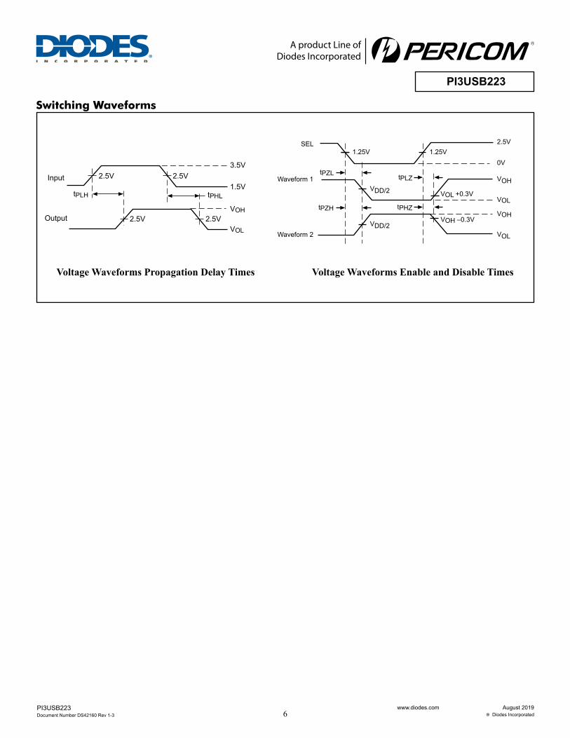
Voltage Waveforms Propagation Delay Times
Switching Waveforms
Voltage Waveforms Enable and Disable Times
tPLZ
1.25V 1.25V 2.5V
VOH
0V
VOL
VDD/2
VDD/2
tPHZ
tPZL
tPZH
Waveform 1
Waveform 2
VOL +0.3V
VOH –0.3V
VOL
VOH
SEL
Input
tPLH
2.5V 2.5V
2.5V 2.5V
tPHL
3.5V
1.5V
OutputVOH
VOL
7
A product Line ofDiodes Incorporated
PI3USB223
www.diodes.com August 2019 Diodes Incorporated
PI3USB223 Document Number DS42160 Rev 1-3
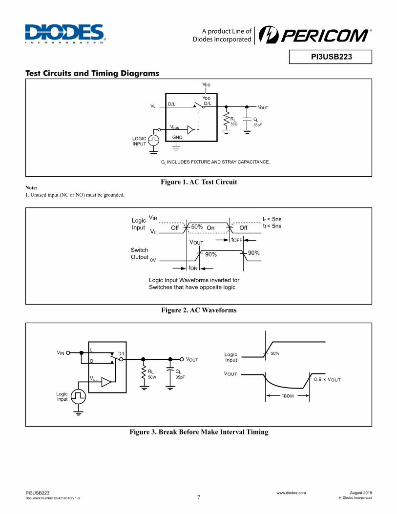
Figure 1. AC Test Circuit
Figure 2. AC Waveforms
Test Circuits and Timing Diagrams
Logic Input Waveforms inverted for Switches that have opposite logic
tON
VOUT
trtf
tOFF
90%90%
< 5ns< 5ns50%
Switch Output
Logic Input
VIH
VIL
0V
Off On Off
Note:1. Unused input (NC or NO) must be grounded.
Figure 3. Break Before Make Interval Timing
CL 35pF
RL50W
tBBM
VOUT 0.9 x VOUT
Logic Input
D/L
Vbus
L
D
VIN
Logic Input
VOUT 50%
LOGICINPUT
RL50Ω
D/L
GND
CL INCLUDES FIXTURE AND STRAY CAPACITANCE.
VN D/LVDD
CL
VDD
VOUT
35pFVbus
8
A product Line ofDiodes Incorporated
PI3USB223
www.diodes.com August 2019 Diodes Incorporated
PI3USB223 Document Number DS42160 Rev 1-3
Figure 4. Charge Injection Test
Figure 5. Off Isolation Figure 6. Crosstalk
Figure 7. Channel Off Capacitance Figure 8. Channel On Capacitance
CL 1nF
D/L
Vbus
VGEN
RGEN
Logic Input
Logic Input
Q = (∆VOUT)(CL)
VOUT OFF ON OFF
∆VOUT
L/D
10nF
GND
VDD
VDD
Logic Input0V or VIH
RL50Ω
SignalGenerator
CL5pF
50Ω
Analyzer
D/L
Vbus
D/L
10nF
GND
VDD
RL50W
Signal Generator
CL5pF
50W
Analyzer
VDD
50W
D/L
Vbus
L
D
CapacitanceMeter
10nF
GND
f = 1 MHz
VDD
VDD
Logic Input0V or VIH
L/D
L/D
Vbus
CapacitanceMeter
10nF
GND
VDD
VDD
f = 1 MHz Logic Input0V or VIH
L/D
Vbus
L/D
9
A product Line ofDiodes Incorporated
PI3USB223
www.diodes.com August 2019 Diodes Incorporated
PI3USB223 Document Number DS42160 Rev 1-3
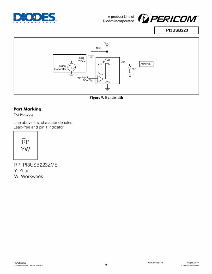
Figure 9. Bandwidth
10nF
GND
Logic Input0V or VIH
VDD
VDD
50ΩSignal
Generator
50Ω
ANALYZERL/D
Vbus
V/D
Part MarkingZM Package
RPYW
RP: PI3USB223ZMEY: YearW: Workweek
Line above first chatacter denotes Lead-free and pin 1 indicator
10
A product Line ofDiodes Incorporated
PI3USB223
www.diodes.com August 2019 Diodes Incorporated
PI3USB223 Document Number DS42160 Rev 1-3
Ordering InformationOrdering Code Package Code Description Top MarkPI3USB223ZMEX ZM 10-contact, Ultra-thin Quad Flat No-Lead (UQFN) RP
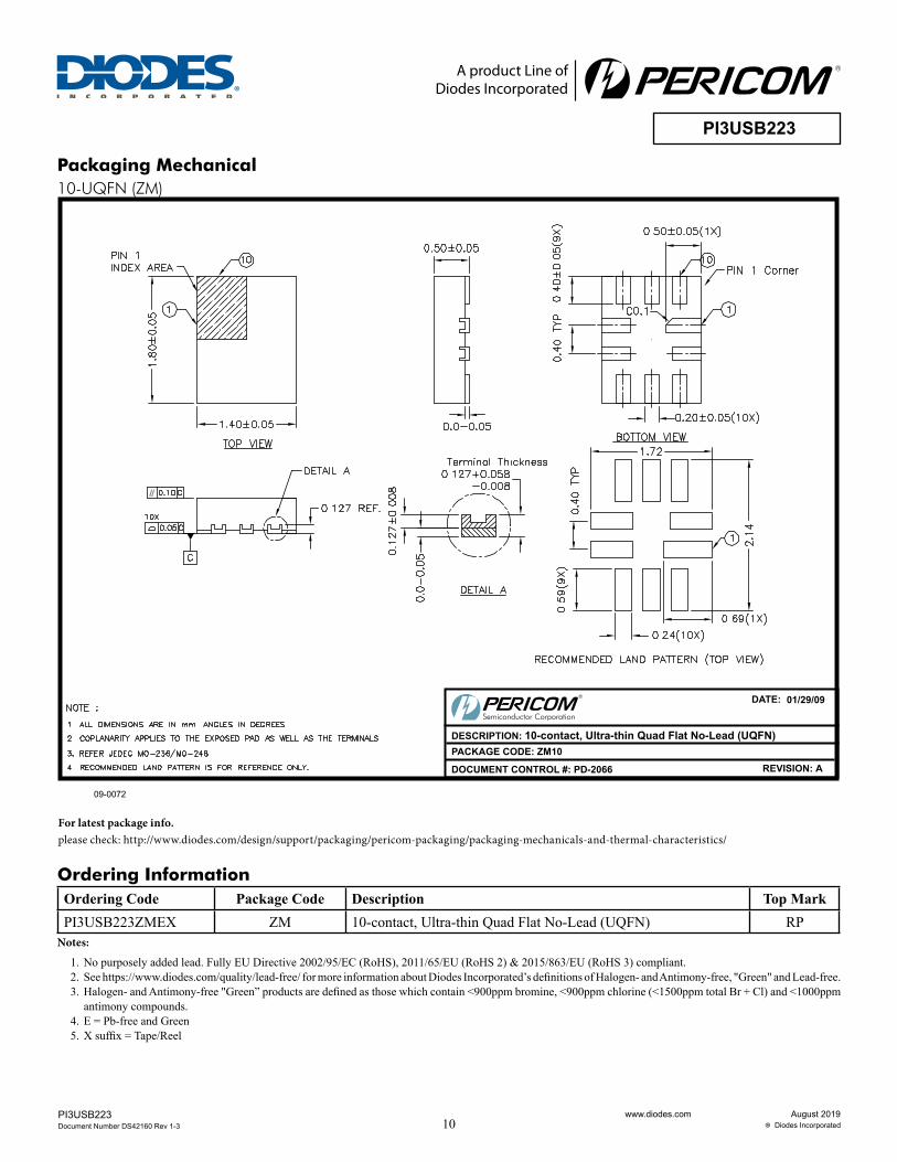
Packaging Mechanical10-UQFN (ZM)
1
DESCRIPTION: 10-contact, Ultra-thin Quad Flat No-Lead (UQFN)PACKAGE CODE: ZM10
DOCUMENT CONTROL #: PD-2066 REVISION: A
DATE: 01/29/09
09-0072
Notes:
1. No purposely added lead. Fully EU Directive 2002/95/EC (RoHS), 2011/65/EU (RoHS 2) & 2015/863/EU (RoHS 3) compliant. 2. See https://www.diodes.com/quality/lead-free/ for more information about Diodes Incorporated’s definitions of Halogen- and Antimony-free, "Green" and Lead-free. 3. Halogen- and Antimony-free "Green” products are defined as those which contain <900ppm bromine, <900ppm chlorine (<1500ppm total Br + Cl) and <1000ppm
antimony compounds.4. E = Pb-free and Green5. X suffix = Tape/Reel
For latest package info. please check: http://www.diodes.com/design/support/packaging/pericom-packaging/packaging-mechanicals-and-thermal-characteristics/
11
A product Line ofDiodes Incorporated
PI3USB223
www.diodes.com August 2019 Diodes Incorporated
PI3USB223 Document Number DS42160 Rev 1-3
IMPORTANT NOTICE
DIODES INCORPORATED MAKES NO WARRANTY OF ANY KIND, EXPRESS OR IMPLIED, WITH REGARDS TO THIS DOCUMENT, INCLUDING, BUT NOT LIMITED TO, THE IMPLIED WARRANTIES OF MERCHANTABILITY AND FITNESS FOR A PARTICULAR PURPOSE (AND THEIR EQUIVALENTS UNDER THE LAWS OF ANY JURISDICTION).
Diodes Incorporated and its subsidiaries reserve the right to make modifications, enhancements, improvements, corrections or other changes without further no-tice to this document and any product described herein. Diodes Incorporated does not assume any liability arising out of the application or use of this document or any product described herein; neither does Diodes Incorporated convey any license under its patent or trademark rights, nor the rights of others. Any Customer or user of this document or products described herein in such applications shall assume all risks of such use and will agree to hold Diodes Incorporated and all the companies whose products are represented on Diodes Incorporated website, harmless against all damages.
Diodes Incorporated does not warrant or accept any liability whatsoever in respect of any products purchased through unauthorized sales channel.
Should Customers purchase or use Diodes Incorporated products for any unintended or unauthorized application, Customers shall indemnify and hold Diodes Incorporated and its representatives harmless against all claims, damages, expenses, and attorney fees arising out of, directly or indirectly, any claim of personal injury or death associated with such unintended or unauthorized application.
Products described herein may be covered by one or more United States, international or foreign patents pending. Product names and markings noted herein may also be covered by one or more United States, international or foreign trademarks.
This document is written in English but may be translated into multiple languages for reference. Only the English version of this document is the final and determi-native format released by Diodes Incorporated.
LIFE SUPPORT
Diodes Incorporated products are specifically not authorized for use as critical components in life support devices or systems without the express written approval of the Chief Executive Officer of Diodes Incorporated. As used herein:
A. Life support devices or systems are devices or systems which:
1. are intended to implant into the body, or
2. support or sustain life and whose failure to perform when properly used in accordance with instructions for use provided in the labeling can be reasonably expected to result in significant injury to the user.
B. A critical component is any component in a life support device or system whose failure to perform can be reasonably expected to cause the
failure of the life support device or to affect its safety or effectiveness.
Customers represent that they have all necessary expertise in the safety and regulatory ramifications of their life support devices or systems, and acknowledge and agree that they are solely responsible for all legal, regulatory and safety-related requirements concerning their products and any use of Diodes Incorporated products in such safety-critical, life support devices or systems, notwithstanding any devices- or systems-related information or support that may be provided by Diodes Incorporated. Further, Customers must fully indemnify Diodes Incorporated and its representatives against any damages arising out of the use of Diodes Incorporated products in such safety-critical, life support devices or systems.
Copyright © 2016, Diodes Incorporated
www.diodes.com