Description Pin Assignments - Diodes Incorporated · 2019-04-11 · When PFI is less than 1.25V,...
14
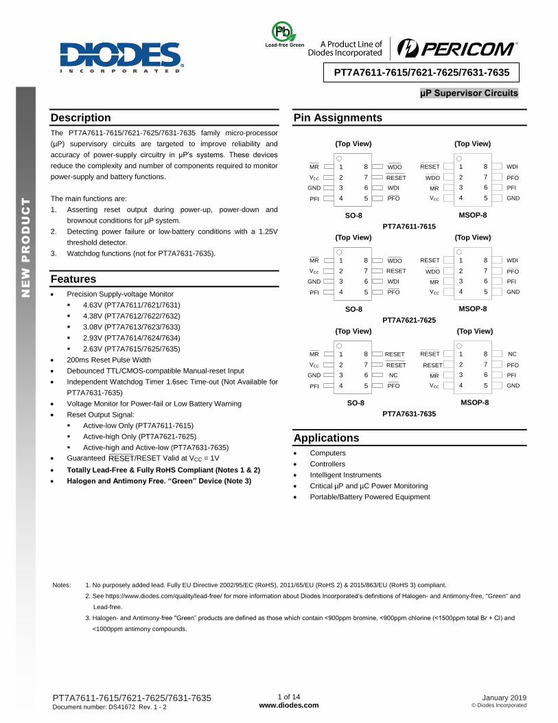
PT7A7611-7615/7621-7625/7631-7635 Document number: DS41672 Rev. 1 - 2 1 of 14 www.diodes.com January 2019 © Diodes Incorporated PT7A7611-7615/7621-7625/7631-7635 NEW PRODUCT μP Supervisor Circuits Description The PT7A7611-7615/7621-7625/7631-7635 family micro-processor (μP) supervisory circuits are targeted to improve reliability and accuracy of power-supply circuitry in µP’s systems. These devices reduce the complexity and number of components required to monitor power-supply and battery functions. The main functions are: 1. Asserting reset output during power-up, power-down and brownout conditions for μP system. 2. Detecting power failure or low-battery conditions with a 1.25V threshold detector. 3. Watchdog functions (not for PT7A7631-7635). Features Precision Supply-voltage Monitor 4.63V (PT7A7611/7621/7631) 4.38V (PT7A7612/7622/7632) 3.08V (PT7A7613/7623/7633) 2.93V (PT7A7614/7624/7634) 2.63V (PT7A7615/7625/7635) 200ms Reset Pulse Width Debounced TTL/CMOS-compatible Manual-reset Input Independent Watchdog Timer 1.6sec Time-out (Not Available for PT7A7631-7635) Voltage Monitor for Power-fail or Low Battery Warning Reset Output Signal: Active-low Only (PT7A7611-7615) Active-high Only (PT7A7621-7625) Active-high and Active-low (PT7A7631-7635) Guaranteed RESET /RESET Valid at VCC = 1V Totally Lead-Free & Fully RoHS Compliant (Notes 1 & 2) Halogen and Antimony Free. “Green” Device (Note 3) Pin Assignments (Top View) (Top View) 1 2 3 4 5 6 7 8 MR VCC GND PFI PFO WDI RESET WDO SO-8 1 2 3 4 5 6 7 8 MR VCC GND PFI PFO WDI RESET WDO MSOP-8 PT7A7611-7615 (Top View) (Top View) 1 2 3 4 5 6 7 8 MR VCC GND PFI PFO WDI RESET WDO SO-8 1 2 3 4 5 6 7 8 MR VCC GND PFI PFO WDI RESET WDO MSOP-8 PT7A7621-7625 (Top View) (Top View) 1 2 3 4 5 6 7 8 MR VCC GND PFI PFO NC RESET RESET SO-8 1 2 3 4 5 6 7 8 MR VCC GND PFI PFO NC RESET RESET MSOP-8 PT7A7631-7635 Applications Computers Controllers Intelligent Instruments Critical μP and μC Power Monitoring Portable/Battery Powered Equipment Notes: 1. No purposely added lead. Fully EU Directive 2002/95/EC (RoHS), 2011/65/EU (RoHS 2) & 2015/863/EU (RoHS 3) compliant. 2. See https://www.diodes.com/quality/lead-free/ for more information about Diodes Incorporated’s definitions of Halogen- and Antimony-free, "Green" and Lead-free. 3. Halogen- and Antimony-free "Green” products are defined as those which contain <900ppm bromine, <900ppm chlorine (<1500ppm total Br + Cl) and <1000ppm antimony compounds.
Transcript of Description Pin Assignments - Diodes Incorporated · 2019-04-11 · When PFI is less than 1.25V,...
PT7A7611-7615/7621-7625/7631-7635 Document number: DS41672 Rev. 1 - 2
1 of 14 www.diodes.com
January 2019 © Diodes Incorporated
PT7A7611-7615/7621-7625/7631-7635
NE
W P
RO
DU
CT
μP Supervisor Circuits
Description
The PT7A7611-7615/7621-7625/7631-7635 family micro-processor
(µP) supervisory circuits are targeted to improve reliability and
accuracy of power-supply circuitry in µP’s systems. These devices
reduce the complexity and number of components required to monitor
power-supply and battery functions.
The main functions are:
1. Asserting reset output during power-up, power-down and
brownout conditions for µP system.
2. Detecting power failure or low-battery conditions with a 1.25V
threshold detector.
3. Watchdog functions (not for PT7A7631-7635).
Features
Precision Supply-voltage Monitor
4.63V (PT7A7611/7621/7631)
4.38V (PT7A7612/7622/7632)
3.08V (PT7A7613/7623/7633)
2.93V (PT7A7614/7624/7634)
2.63V (PT7A7615/7625/7635)
200ms Reset Pulse Width
Debounced TTL/CMOS-compatible Manual-reset Input
Independent Watchdog Timer 1.6sec Time-out (Not Available for
PT7A7631-7635)
Voltage Monitor for Power-fail or Low Battery Warning
Reset Output Signal:
Active-low Only (PT7A7611-7615)
Active-high Only (PT7A7621-7625)
Active-high and Active-low (PT7A7631-7635)
Guaranteed RESET/RESET Valid at VCC = 1V
Totally Lead-Free & Fully RoHS Compliant (Notes 1 & 2)
Halogen and Antimony Free. “Green” Device (Note 3)
Pin Assignments
(Top View)
(Top View)
1
2
3
4 5
6
7
8MR
VCC
GND
PFI PFO
WDI
RESET
WDO
SO-8
1
2
3
4 5
6
7
8
MR
VCC GND
PFI
PFO
WDIRESET
WDO
MSOP-8
PT7A7611-7615
(Top View) (Top View)
1
2
3
4 5
6
7
8MR
VCC
GND
PFI PFO
WDI
RESET
WDO
SO-8
1
2
3
4 5
6
7
8
MR
VCC GND
PFI
PFO
WDIRESET
WDO
MSOP-8
PT7A7621-7625
(Top View) (Top View)
1
2
3
4 5
6
7
8MR
VCC
GND
PFI PFO
NC
RESET
RESET
SO-8
1
2
3
4 5
6
7
8
MR
VCC GND
PFI
PFO
NCRESET
RESET
MSOP-8
PT7A7631-7635
Applications
Computers
Controllers
Intelligent Instruments
Critical µP and µC Power Monitoring
Portable/Battery Powered Equipment
Notes: 1. No purposely added lead. Fully EU Directive 2002/95/EC (RoHS), 2011/65/EU (RoHS 2) & 2015/863/EU (RoHS 3) compliant.
2. See https://www.diodes.com/quality/lead-free/ for more information about Diodes Incorporated’s definitions of Halogen- and Antimony-free, "Green" and
Lead-free.
3. Halogen- and Antimony-free "Green” products are defined as those which contain <900ppm bromine, <900ppm chlorine (<1500ppm total Br + Cl) and
<1000ppm antimony compounds.
PT7A7611-7615/7621-7625/7631-7635 Document number: DS41672 Rev. 1 - 2
2 of 14 www.diodes.com
January 2019 © Diodes Incorporated
PT7A7611-7615/7621-7625/7631-7635
NE
W P
RO
DU
CT
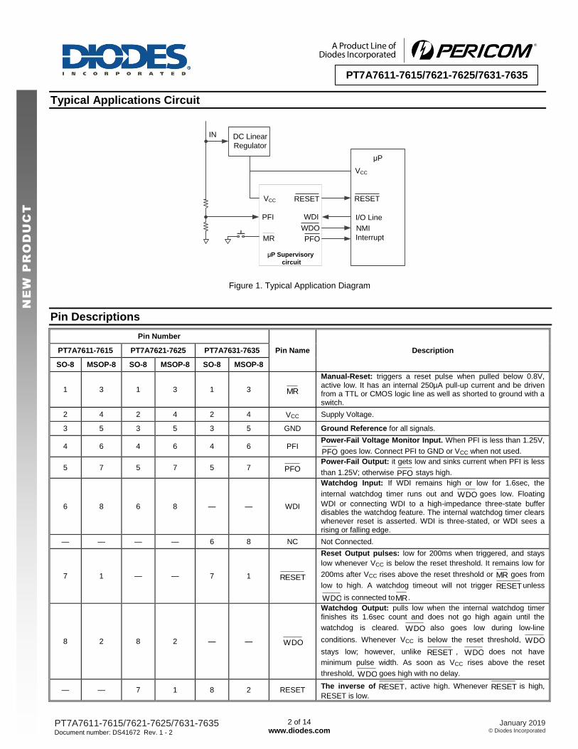
Typical Applications Circuit
MR
VCC
PFI
RESET
WDI
WDO
PFO
RESET
I/O Line
NMI
Interrupt
μP
DC Linear
Regulator
VCC
IN
μP Supervisory
circuit
Figure 1. Typical Application Diagram
Pin Descriptions
Pin Number
Pin Name Description PT7A7611-7615 PT7A7621-7625 PT7A7631-7635
SO-8 MSOP-8 SO-8 MSOP-8 SO-8 MSOP-8
1 3 1 3 1 3 MR
Manual-Reset: triggers a reset pulse when pulled below 0.8V, active low. It has an internal 250µA pull-up current and be driven from a TTL or CMOS logic line as well as shorted to ground with a switch.
2 4 2 4 2 4 VCC Supply Voltage.
3 5 3 5 3 5 GND Ground Reference for all signals.
4 6 4 6 4 6 PFI Power-Fail Voltage Monitor Input. When PFI is less than 1.25V,
PFO goes low. Connect PFI to GND or VCC when not used.
5 7 5 7 5 7 PFO Power-Fail Output: it gets low and sinks current when PFI is less
than 1.25V; otherwise PFO stays high.
6 8 6 8 — — WDI
Watchdog Input: If WDI remains high or low for 1.6sec, the
internal watchdog timer runs out and WDO goes low. Floating
WDI or connecting WDI to a high-impedance three-state buffer disables the watchdog feature. The internal watchdog timer clears whenever reset is asserted. WDI is three-stated, or WDI sees a rising or falling edge.
— — — — 6 8 NC Not Connected.
7 1 — — 7 1 RESET
Reset Output pulses: low for 200ms when triggered, and stays
low whenever VCC is below the reset threshold. It remains low for
200ms after VCC rises above the reset threshold or MR goes from
low to high. A watchdog timeout will not trigger RESETunless
WDO is connected toMR.
8 2 8 2 — — WDO
Watchdog Output: pulls low when the internal watchdog timer finishes its 1.6sec count and does not go high again until the
watchdog is cleared. WDO also goes low during low-line
conditions. Whenever VCC is below the reset threshold, WDO
stays low; however, unlike RESET , WDO does not have
minimum pulse width. As soon as VCC rises above the reset
threshold, WDO goes high with no delay.
— — 7 1 8 2 RESET The inverse of RESET, active high. Whenever RESET is high,
RESET is low.
PT7A7611-7615/7621-7625/7631-7635 Document number: DS41672 Rev. 1 - 2
3 of 14 www.diodes.com
January 2019 © Diodes Incorporated
PT7A7611-7615/7621-7625/7631-7635
NE
W P
RO
DU
CT
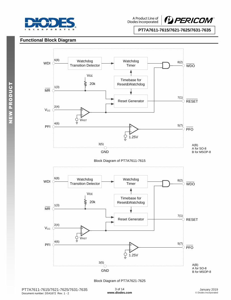
Functional Block Diagram
Watchdog
Transition Detector
Watchdog
Timer
Timebase for
Reset&Watchdog
Reset Generator
20k
VRST
1.25V
Vcc
MR
VCC
PFI
WDO
PFO
RESET
WDI6(8)
1(3)
2(4)
4(6)5(7)
7(1)
8(2)
GND
3(5)
Block Diagram of PT7A7611-7615
Watchdog
Transition Detector
Watchdog
Timer
Timebase for
Reset&Watchdog
Reset Generator
20k
VRST
1.25V
Vcc
MR
VCC
PFI
WDO
PFO
RESET
WDI6(8)
1(3)
2(4)
4(6)5(7)
7(1)
8(2)
GND
3(5)
Block Diagram of PT7A7621-7625
A(B) A for SO-8 B for MSOP-8
A(B) A for SO-8 B for MSOP-8
PT7A7611-7615/7621-7625/7631-7635 Document number: DS41672 Rev. 1 - 2
4 of 14 www.diodes.com
January 2019 © Diodes Incorporated
PT7A7611-7615/7621-7625/7631-7635
NE
W P
RO
DU
CT
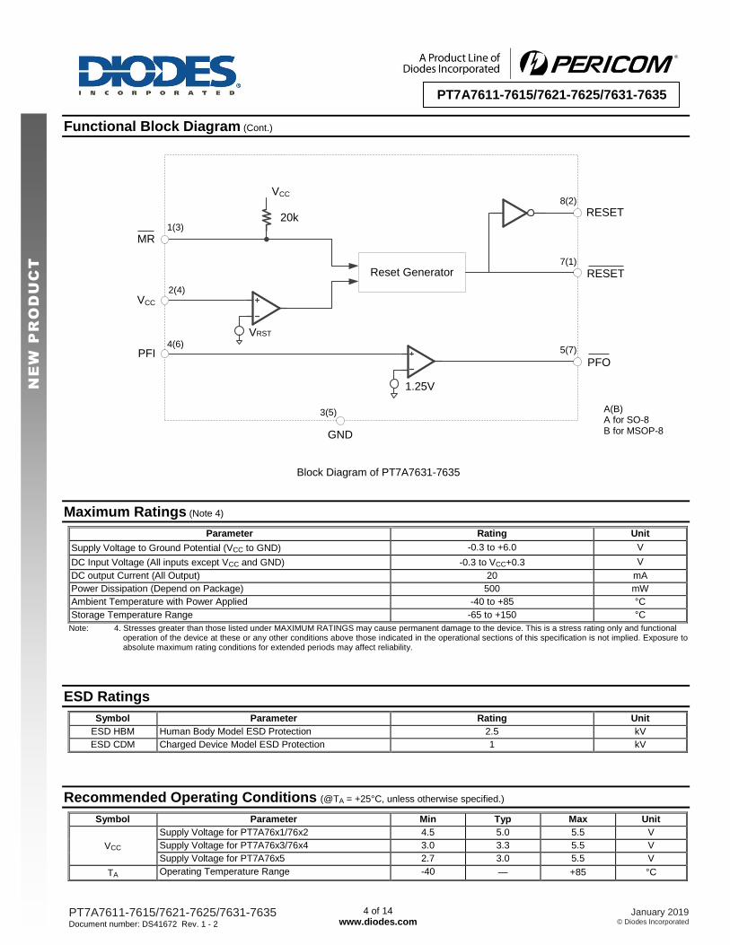
Functional Block Diagram (Cont.)
Reset Generator
20k
VRST
1.25V
VCC
MR
VCC
PFIPFO
RESET
RESET
1(3)
2(4)
4(6)5(7)
7(1)
8(2)
GND
3(5)
Block Diagram of PT7A7631-7635
Maximum Ratings (Note 4)
Parameter Rating Unit
Supply Voltage to Ground Potential (VCC to GND) -0.3 to +6.0 V
DC Input Voltage (All inputs except VCC and GND) -0.3 to VCC+0.3 V
DC output Current (All Output) 20 mA
Power Dissipation (Depend on Package) 500 mW
Ambient Temperature with Power Applied -40 to +85 °C
Storage Temperature Range -65 to +150 °C
Note: 4. Stresses greater than those listed under MAXIMUM RATINGS may cause permanent damage to the device. This is a stress rating only and functional operation of the device at these or any other conditions above those indicated in the operational sections of this specification is not implied. Exposure to absolute maximum rating conditions for extended periods may affect reliability.
ESD Ratings
Symbol Parameter Rating Unit
ESD HBM Human Body Model ESD Protection 2.5 kV
ESD CDM Charged Device Model ESD Protection 1 kV
Recommended Operating Conditions (@TA = +25°C, unless otherwise specified.)
Symbol Parameter Min Typ Max Unit
VCC
Supply Voltage for PT7A76x1/76x2 4.5 5.0 5.5 V
Supply Voltage for PT7A76x3/76x4 3.0 3.3 5.5 V
Supply Voltage for PT7A76x5 2.7 3.0 5.5 V
TA Operating Temperature Range -40 — +85 °C
A(B) A for SO-8 B for MSOP-8
PT7A7611-7615/7621-7625/7631-7635 Document number: DS41672 Rev. 1 - 2
5 of 14 www.diodes.com
January 2019 © Diodes Incorporated
PT7A7611-7615/7621-7625/7631-7635
NE
W P
RO
DU
CT
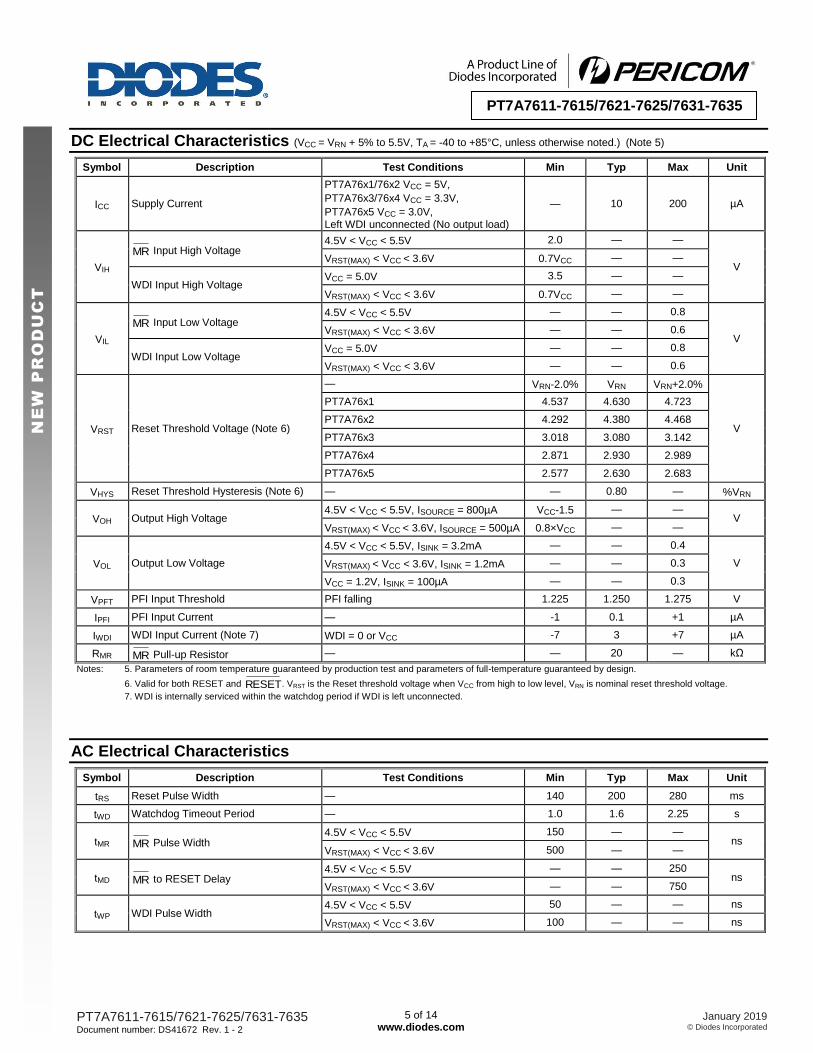
DC Electrical Characteristics (VCC = VRN + 5% to 5.5V, TA = -40 to +85°C, unless otherwise noted.) (Note 5)
Symbol Description Test Conditions Min Typ Max Unit
ICC Supply Current
PT7A76x1/76x2 VCC = 5V,
PT7A76x3/76x4 VCC = 3.3V,
PT7A76x5 VCC = 3.0V, Left WDI unconnected (No output load)
— 10 200 µA
VIH
MR Input High Voltage 4.5V < VCC < 5.5V 2.0 — —
V VRST(MAX) < VCC < 3.6V 0.7VCC — —
WDI Input High Voltage VCC = 5.0V 3.5 — —
VRST(MAX) < VCC < 3.6V 0.7VCC — —
VIL
MR Input Low Voltage 4.5V < VCC < 5.5V — — 0.8
V VRST(MAX) < VCC < 3.6V — — 0.6
WDI Input Low Voltage VCC = 5.0V — — 0.8
VRST(MAX) < VCC < 3.6V — — 0.6
VRST Reset Threshold Voltage (Note 6)
— VRN-2.0% VRN VRN+2.0%
V
PT7A76x1 4.537 4.630 4.723
PT7A76x2 4.292 4.380 4.468
PT7A76x3 3.018 3.080 3.142
PT7A76x4 2.871 2.930 2.989
PT7A76x5 2.577 2.630 2.683
VHYS Reset Threshold Hysteresis (Note 6) — — 0.80 — %VRN
VOH Output High Voltage 4.5V < VCC < 5.5V, ISOURCE = 800µA VCC-1.5 — —
V VRST(MAX) < VCC < 3.6V, ISOURCE = 500µA 0.8×VCC — —
VOL Output Low Voltage
4.5V < VCC < 5.5V, ISINK = 3.2mA — — 0.4
V VRST(MAX) < VCC < 3.6V, ISINK = 1.2mA — — 0.3
VCC = 1.2V, ISINK = 100µA — — 0.3
VPFT PFI Input Threshold PFI falling 1.225 1.250 1.275 V
IPFI PFI Input Current — -1 0.1 +1 µA
IWDI WDI Input Current (Note 7) WDI = 0 or VCC -7 3 +7 µA
RMR MR Pull-up Resistor — — 20 — kΩ
Notes: 5. Parameters of room temperature guaranteed by production test and parameters of full-temperature guaranteed by design.
6. Valid for both RESET and RESET. VRST is the Reset threshold voltage when VCC from high to low level, VRN is nominal reset threshold voltage.
7. WDI is internally serviced within the watchdog period if WDI is left unconnected.
AC Electrical Characteristics
Symbol Description Test Conditions Min Typ Max Unit
tRS Reset Pulse Width — 140 200 280 ms
tWD Watchdog Timeout Period — 1.0 1.6 2.25 s
tMR MR Pulse Width 4.5V < VCC < 5.5V 150 — —
ns VRST(MAX) < VCC < 3.6V 500 — —
tMD MR to RESET Delay 4.5V < VCC < 5.5V — — 250
ns VRST(MAX) < VCC < 3.6V — — 750
tWP WDI Pulse Width 4.5V < VCC < 5.5V 50 — — ns
VRST(MAX) < VCC < 3.6V 100 — — ns
PT7A7611-7615/7621-7625/7631-7635 Document number: DS41672 Rev. 1 - 2
6 of 14 www.diodes.com
January 2019 © Diodes Incorporated
PT7A7611-7615/7621-7625/7631-7635
NE
W P
RO
DU
CT
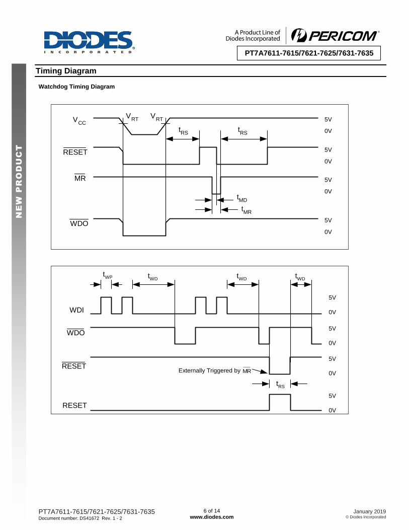
Timing Diagram
Watchdog Timing Diagram
t WP t WD t WD t WD
t RS
WDI
WDO
RESET
RESET
5V
0V
5V
0V
5V
0V
5V
0V
Externally Triggered by MR
V RT
t RS t
RS
t MR
t MD
WDO
RESET
MR
5V
0V
V RT V
CC
5V
0V
5V
0V
5V
0V
PT7A7611-7615/7621-7625/7631-7635 Document number: DS41672 Rev. 1 - 2
7 of 14 www.diodes.com
January 2019 © Diodes Incorporated
PT7A7611-7615/7621-7625/7631-7635
NE
W P
RO
DU
CT
Functional Description
The PT7A7611-7615/7621-7625/7631-7635 family can assert reset output during power-up, power-down and brownout conditions for µP system,
detect power failure or low-battery conditions with a 1.25V threshold detector and have watchdog functions. Refer to Function Comparison Table
of PT7A7611-7615/7621-7625/7631-7635 family for their individual features. Figure 1 shows typical application.
Reset Output
The supervisory circuits can assert reset for a microprocessor during power-up, power-down and brownout to prevent code execution errors.
On power-up, once VCC reaches about 1.0V, RESETis a guaranteed logic low of 0.4V or less. As VCC rises, RESET stays low. When VCC rises
above the reset threshold, an internal timer releases RESET after about 200ms. RESETpulses low whenever VCC drops below the reset
threshold, i.e. brownout condition. If brownout occurs in the middle of a previously initiated reset pulse, the pulse continues for at least another
140ms. On power-down, once VCC falls below the reset threshold, RESET stays low and is guaranteed to be 0.4V or less until VCC drops below
1.0V.
The PT7A7621-7625 and PT7A7631-7635 active-high RESET output is simply the inverse of the RESEToutput, and is guaranteed to be valid
with VCC down to 1.2V. Some μPs, such as Intel’s 80C51, require an active-high reset pulse.
Watchdog Timer
The watchdog circuit monitors the μP activity. If the μP does not toggle the watchdog input (WDI) within 1.6sec and WDI is not in high impedance,
WDO goes low. As long as RESET is asserted or the WDI input is in high impedance, the watchdog timer will stay cleared and will not count. As
soon as reset is released and WDI is driven high or low, the timer will start counting. Pulses as short as 50ns can be detected.
Typically, WDO will be connected to the non-maskable interrupt input (NMI) of a μP. When VCC drops below the reset threshold, WDO will go low
whether or not the watchdog timer has timed out yet. Normally this would trigger an NMI interrupt, but RESET goes low simultaneously, and thus
overrides the NMI interrupt. If WDI is left unconnected, WDO can be used as a low-line output. Since floating WDI disables the internal timer,
WDO goes low only when VCC falls below the reset threshold, thus functioning as a low-line output.
Manual Reset
The manual-reset input (MR) allows reset to be triggered by a push button switch. The switch is effectively debounced by the 140ms minimum
reset pulse width. MR is TTL/CMOS logic compatible, so it can be driven by any logic reset output.
Power-Fail Comparator
The power-fail comparator will send out a Low signal once detects a voltage lowered than 1.25V. It can be used for various purposes because its
output and non-inverting input are not internally connected. The inverting input is internally connected to a 1.25V reference.
PT7A7611-7615/7621-7625/7631-7635 Document number: DS41672 Rev. 1 - 2
8 of 14 www.diodes.com
January 2019 © Diodes Incorporated
PT7A7611-7615/7621-7625/7631-7635
NE
W P
RO
DU
CT
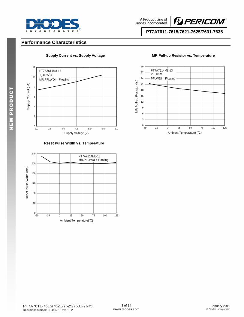
Performance Characteristics
Supply Current vs. Supply Voltage MR Pull-up Resistor vs. Temperature
Reset Pulse Width vs. Temperature
3.0 3.5 4.0 4.5 5.0 5.5 6.00
2
4
6
8
10
12
Sup
ply
Cu
rre
nt (A
)
Supply Voltage (V)
PT7A7614M8-13
TA = 25
oC
MR,PFI,WDI = Floating
-50 -25 0 25 50 75 100 1250
3
6
9
12
15
18
21
24
27
30
MR
Pu
ll-u
p R
esis
tor
(k
)
Ambient Temperature (oC)
PT7A7614M8-13V
CC = 5V
PFI,WDI = Floating
-50 -25 0 25 50 75 100 1250
40
80
120
160
200
240
Re
se
t P
uls
e W
idth
(m
s)
Ambient Temperature(oC)
PT7A7614M8-13MR,PFI,WDI = Floating
PT7A7611-7615/7621-7625/7631-7635 Document number: DS41672 Rev. 1 - 2
9 of 14 www.diodes.com
January 2019 © Diodes Incorporated
PT7A7611-7615/7621-7625/7631-7635
NE
W P
RO
DU
CT
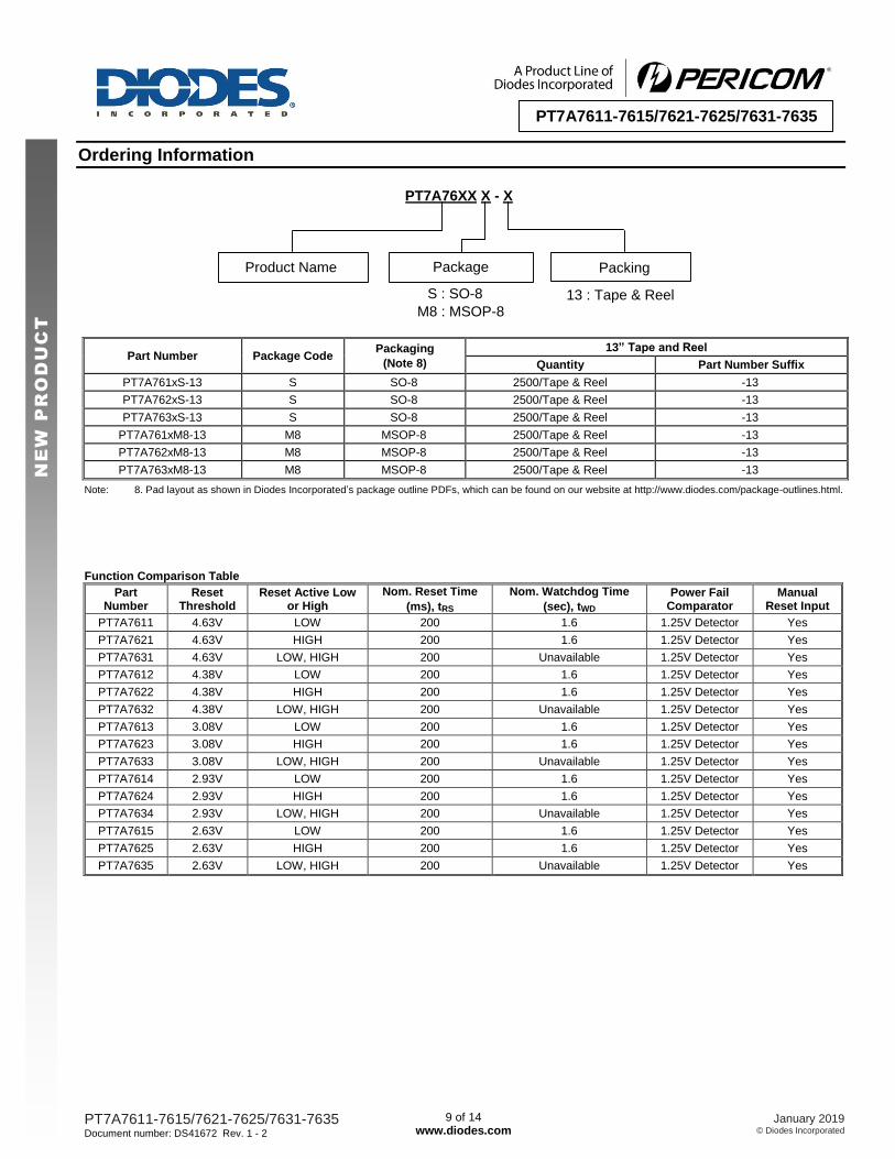
Ordering Information
PT7A76XX X - X
PackingProduct Name Package
13 : Tape & ReelS : SO-8
M8 : MSOP-8
Part Number Package Code Packaging
(Note 8)
13” Tape and Reel
Quantity Part Number Suffix
PT7A761xS-13 S SO-8 2500/Tape & Reel -13
PT7A762xS-13 S SO-8 2500/Tape & Reel -13
PT7A763xS-13 S SO-8 2500/Tape & Reel -13
PT7A761xM8-13 M8 MSOP-8 2500/Tape & Reel -13
PT7A762xM8-13 M8 MSOP-8 2500/Tape & Reel -13
PT7A763xM8-13 M8 MSOP-8 2500/Tape & Reel -13
Note: 8. Pad layout as shown in Diodes Incorporated’s package outline PDFs, which can be found on our website at http://www.diodes.com/package-outlines.html.
Function Comparison Table
Part Number
Reset Threshold
Reset Active Low or High
Nom. Reset Time
(ms), tRS
Nom. Watchdog Time
(sec), tWD
Power Fail Comparator
Manual Reset Input
PT7A7611 4.63V LOW 200 1.6 1.25V Detector Yes
PT7A7621 4.63V HIGH 200 1.6 1.25V Detector Yes
PT7A7631 4.63V LOW, HIGH 200 Unavailable 1.25V Detector Yes
PT7A7612 4.38V LOW 200 1.6 1.25V Detector Yes
PT7A7622 4.38V HIGH 200 1.6 1.25V Detector Yes
PT7A7632 4.38V LOW, HIGH 200 Unavailable 1.25V Detector Yes
PT7A7613 3.08V LOW 200 1.6 1.25V Detector Yes
PT7A7623 3.08V HIGH 200 1.6 1.25V Detector Yes
PT7A7633 3.08V LOW, HIGH 200 Unavailable 1.25V Detector Yes
PT7A7614 2.93V LOW 200 1.6 1.25V Detector Yes
PT7A7624 2.93V HIGH 200 1.6 1.25V Detector Yes
PT7A7634 2.93V LOW, HIGH 200 Unavailable 1.25V Detector Yes
PT7A7615 2.63V LOW 200 1.6 1.25V Detector Yes
PT7A7625 2.63V HIGH 200 1.6 1.25V Detector Yes
PT7A7635 2.63V LOW, HIGH 200 Unavailable 1.25V Detector Yes
PT7A7611-7615/7621-7625/7631-7635 Document number: DS41672 Rev. 1 - 2
10 of 14 www.diodes.com
January 2019 © Diodes Incorporated
PT7A7611-7615/7621-7625/7631-7635
NE
W P
RO
DU
CT
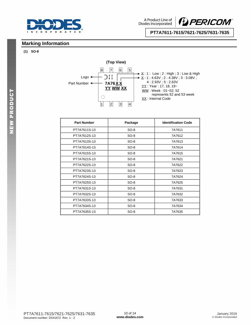
Marking Information
(1) SO-8
7A76 X X
(Top View)
YY WW XX
Part Number
Logo
8 7 6 5
1 2 3 4
WW : Week : 01~52; 52
YY : Year : 17, 18, 19~
XX : Internal Code
represents 52 and 53 week
X : 1 : Low ; 2 : High ; 3 : Low & High
X : 1 : 4.63V ; 2 : 4.38V ; 3 : 3.08V ;
4 : 2.93V ; 5 : 2.63V
Part Number Package Identification Code
PT7A7611S-13 SO-8 7A7611
PT7A7612S-13 SO-8 7A7612
PT7A7613S-13 SO-8 7A7613
PT7A7614S-13 SO-8 7A7614
PT7A7615S-13 SO-8 7A7615
PT7A7621S-13 SO-8 7A7621
PT7A7622S-13 SO-8 7A7622
PT7A7623S-13 SO-8 7A7623
PT7A7624S-13 SO-8 7A7624
PT7A7625S-13 SO-8 7A7625
PT7A7631S-13 SO-8 7A7631
PT7A7632S-13 SO-8 7A7632
PT7A7633S-13 SO-8 7A7633
PT7A7634S-13 SO-8 7A7634
PT7A7635S-13 SO-8 7A7635
PT7A7611-7615/7621-7625/7631-7635 Document number: DS41672 Rev. 1 - 2
11 of 14 www.diodes.com
January 2019 © Diodes Incorporated
PT7A7611-7615/7621-7625/7631-7635
NE
W P
RO
DU
CT
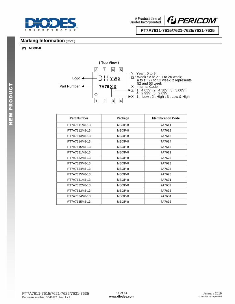
Marking Information (Cont.)
(2) MSOP-8
7A76 X X
( Top View )
Y W X
Part Number
Logo
8 7 6 5
1 2 3 4
Y : Year : 0 to 9
X : Internal Code
a to z : 27 to 52 week; z represents W : Week : A to Z : 1 to 26 week;
52 and 53 week
X : 1 : 4.63V ; 2 : 4.38V ; 3 : 3.08V ; 4 : 2.93V ; 5 : 2.63V
X : 1 : Low ; 2 : High ; 3 : Low & High
Part Number Package Identification Code
PT7A7611M8-13 MSOP-8 7A7611
PT7A7612M8-13 MSOP-8 7A7612
PT7A7613M8-13 MSOP-8 7A7613
PT7A7614M8-13 MSOP-8 7A7614
PT7A7615M8-13 MSOP-8 7A7615
PT7A7621M8-13 MSOP-8 7A7621
PT7A7622M8-13 MSOP-8 7A7622
PT7A7623M8-13 MSOP-8 7A7623
PT7A7624M8-13 MSOP-8 7A7624
PT7A7625M8-13 MSOP-8 7A7625
PT7A7631M8-13 MSOP-8 7A7631
PT7A7632M8-13 MSOP-8 7A7632
PT7A7633M8-13 MSOP-8 7A7633
PT7A7634M8-13 MSOP-8 7A7634
PT7A7635M8-13 MSOP-8 7A7635

PT7A7611-7615/7621-7625/7631-7635 Document number: DS41672 Rev. 1 - 2
12 of 14 www.diodes.com
January 2019 © Diodes Incorporated
PT7A7611-7615/7621-7625/7631-7635
NE
W P
RO
DU
CT
Package Outline Dimensions
Please see http://www.diodes.com/package-outlines.html for the latest version. (1) Package Type: SO-8
1
b
e
E
A
A1
9° (All sides)
4° ± 3°
c
Qh
45°
R 0.1
7°
D
E0
E1
LSeating Plane
Gauge Plane
(2) Package Type: MSOP-8
A
A1
A2
e
Seating Plane
Gauge Plane
0.25
L
4X10°
4X10°
See Detail C
Detail C
c
a
E1
E3
A3
1
E
y
x
D
b
SO-8
Dim Min Max Typ
A 1.40 1.50 1.45
A1 0.10 0.20 0.15
b 0.30 0.50 0.40
c 0.15 0.25 0.20
D 4.85 4.95 4.90
E 5.90 6.10 6.00
E1 3.80 3.90 3.85
E0 3.85 3.95 3.90
e -- -- 1.27
h - -- 0.35
L 0.62 0.82 0.72
Q 0.60 0.70 0.65
All Dimensions in mm
MSOP-8
Dim Min Max Typ
A - 1.10 -
A1 0.05 0.15 0.10
A2 0.75 0.95 0.86
A3 0.29 0.49 0.39
b 0.22 0.38 0.30
c 0.08 0.23 0.15
D 2.90 3.10 3.00
E 4.70 5.10 4.90
E1 2.90 3.10 3.00
E3 2.85 3.05 2.95
e - - 0.65
L 0.40 0.80 0.60
a 0° 8° 4°
x - - 0.750
y - - 0.750
All Dimensions in mm
PT7A7611-7615/7621-7625/7631-7635 Document number: DS41672 Rev. 1 - 2
13 of 14 www.diodes.com
January 2019 © Diodes Incorporated
PT7A7611-7615/7621-7625/7631-7635
NE
W P
RO
DU
CT
Suggested Pad Layout Please see http://www.diodes.com/package-outlines.html for the latest version.
(1) Package Type: SO-8
C X
Y
Y1
X1
(2) Package Type: MSOP-8
X C
Y
Y1
Dimensions Value (in mm)
C 1.27
X 0.802
X1 4.612
Y 1.505
Y1 6.50
Dimensions Value
(in mm)
C 0.650
X 0.450
Y 1.350
Y1 5.300
PT7A7611-7615/7621-7625/7631-7635 Document number: DS41672 Rev. 1 - 2
14 of 14 www.diodes.com
January 2019 © Diodes Incorporated
PT7A7611-7615/7621-7625/7631-7635
NE
W P
RO
DU
CT
IMPORTANT NOTICE DIODES INCORPORATED MAKES NO WARRANTY OF ANY KIND, EXPRESS OR IMPLIED, WITH REGARDS TO THIS DOCUMENT, INCLUDING, BUT NOT LIMITED TO, THE IMPLIED WARRANTIES OF MERCHANTABILITY AND FITNESS FOR A PARTICULAR PURPOSE (AND THEIR EQUIVALENTS UNDER THE LAWS OF ANY JURISDICTION). Diodes Incorporated and its subsidiaries reserve the right to make modifications, enhancements, improvements, corrections or other changes without further notice to this document and any product described herein. Diodes Incorporated does not assume any liability arising out of the application or use of this document or any product described herein; neither does Diodes Incorporated convey any license under its patent or trademark rights, nor the rights of others. Any Customer or user of this document or products described herein in such applications shall assume all risks of such use and will agree to hold Diodes Incorporated and all the companies whose products are represented on Diodes Incorporated website, harmless against all damages. Diodes Incorporated does not warrant or accept any liability whatsoever in respect of any products purchased through unauthorized sales channel. Should Customers purchase or use Diodes Incorporated products for any unintended or unauthorized application, Customers shall indemnify and hold Diodes Incorporated and its representatives harmless against all claims, damages, expenses, and attorney fees arising out of, directly or indirectly, any claim of personal injury or death associated with such unintended or unauthorized application. Products described herein may be covered by one or more United States, international or foreign patents pending. Product names and markings noted herein may also be covered by one or more United States, international or foreign trademarks. This document is written in English but may be translated into multiple languages for reference. Only the English version of this document is the final and determinative format released by Diodes Incorporated.
LIFE SUPPORT Diodes Incorporated products are specifically not authorized for use as critical components in life support devices or systems without the express written approval of the Chief Executive Officer of Diodes Incorporated. As used herein: A. Life support devices or systems are devices or systems which: 1. are intended to implant into the body, or
2. support or sustain life and whose failure to perform when properly used in accordance with instructions for use provided in the labeling can be reasonably expected to result in significant injury to the user.
B. A critical component is any component in a life support device or system whose failure to perform can be reasonably expected to cause the failure of the life support device or to affect its safety or effectiveness. Customers represent that they have all necessary expertise in the safety and regulatory ramifications of their life support devices or systems, and acknowledge and agree that they are solely responsible for all legal, regulatory and safety-related requirements concerning their products and any use of Diodes Incorporated products in such safety-critical, life support devices or systems, notwithstanding any devices- or systems-related information or support that may be provided by Diodes Incorporated. Further, Customers must fully indemnify Diodes Incorporated and its representatives against any damages arising out of the use of Diodes Incorporated products in such safety-critical, life support devices or systems. Copyright © 2019, Diodes Incorporated www.diodes.com