SEMICONDUCTOR DETECTORSbevan/teaching/SemiconductorDetectors.pdf · • Semiconductors • p-n...
48
PEDAGOGICAL REVIEW OF ASPECTS OF ORGANIC AND INORGANIC DEVICES. SEMICONDUCTOR DETECTORS Adrian Bevan [email protected]
Transcript of SEMICONDUCTOR DETECTORSbevan/teaching/SemiconductorDetectors.pdf · • Semiconductors • p-n...
PEDAGOGICAL REVIEW OF ASPECTS OF ORGANIC AND INORGANIC DEVICES.
SEMICONDUCTOR DETECTORS
Adrian Bevan [email protected]
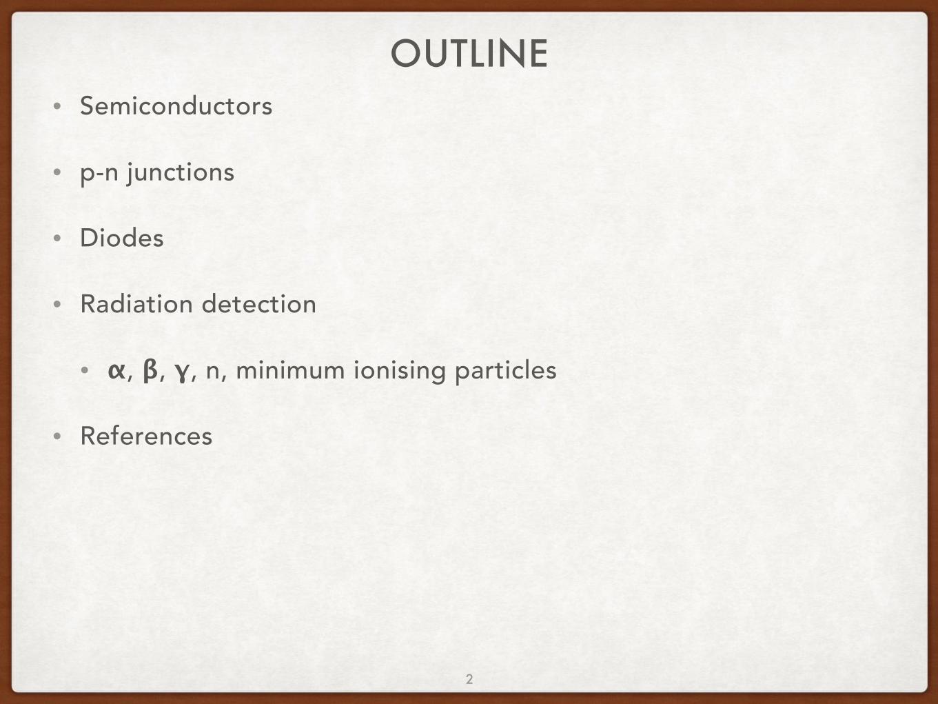
OUTLINE• Semiconductors
• p-n junctions
• Diodes
• Radiation detection
• α, β, γ, n, minimum ionising particles
• References
2
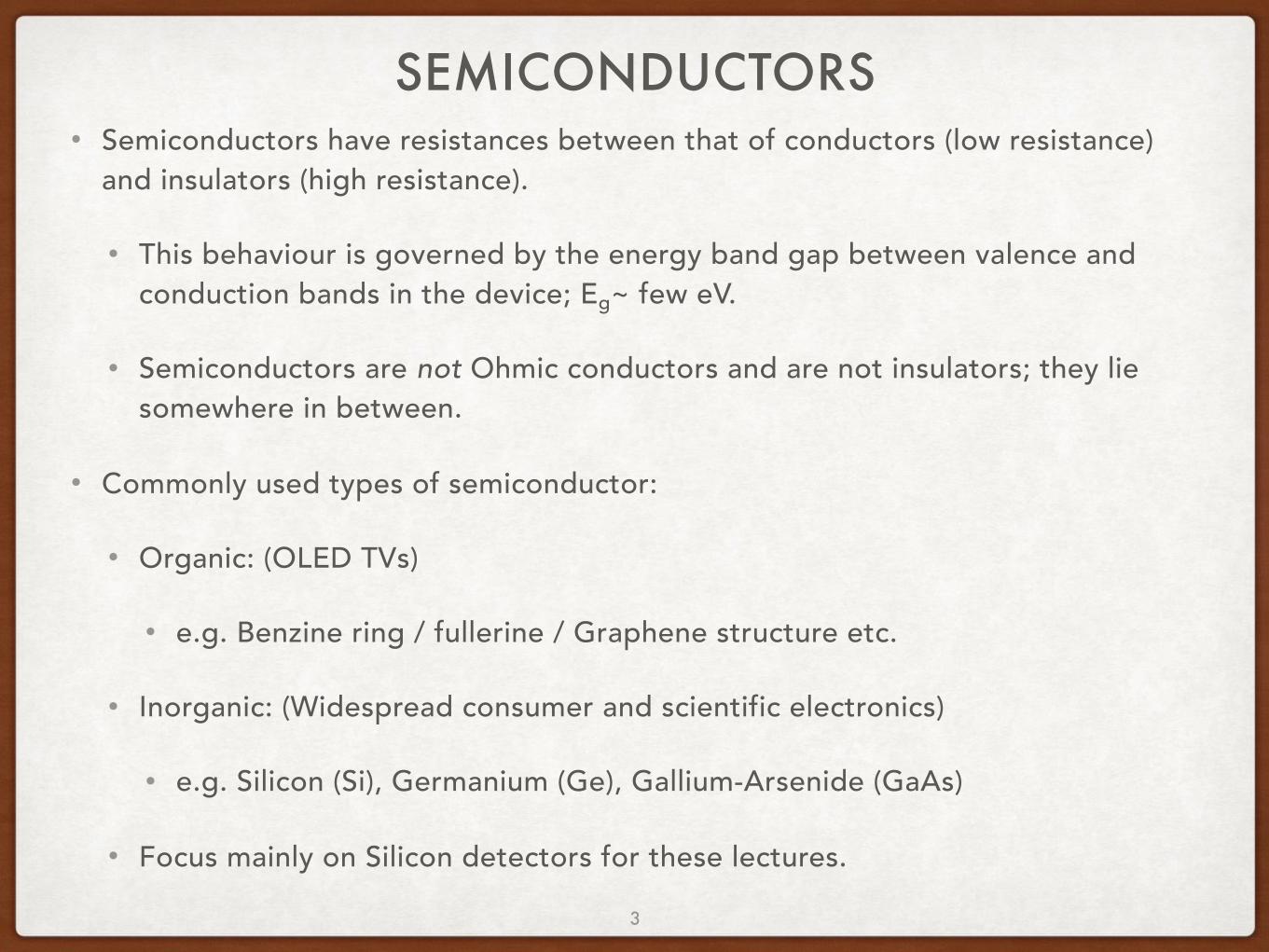
SEMICONDUCTORS• Semiconductors have resistances between that of conductors (low resistance)
and insulators (high resistance).
• This behaviour is governed by the energy band gap between valence and conduction bands in the device; Eg~ few eV.
• Semiconductors are not Ohmic conductors and are not insulators; they lie somewhere in between.
• Commonly used types of semiconductor:
• Organic: (OLED TVs)
• e.g. Benzine ring / fullerine / Graphene structure etc.
• Inorganic: (Widespread consumer and scientific electronics)
• e.g. Silicon (Si), Germanium (Ge), Gallium-Arsenide (GaAs)
• Focus mainly on Silicon detectors for these lectures.3
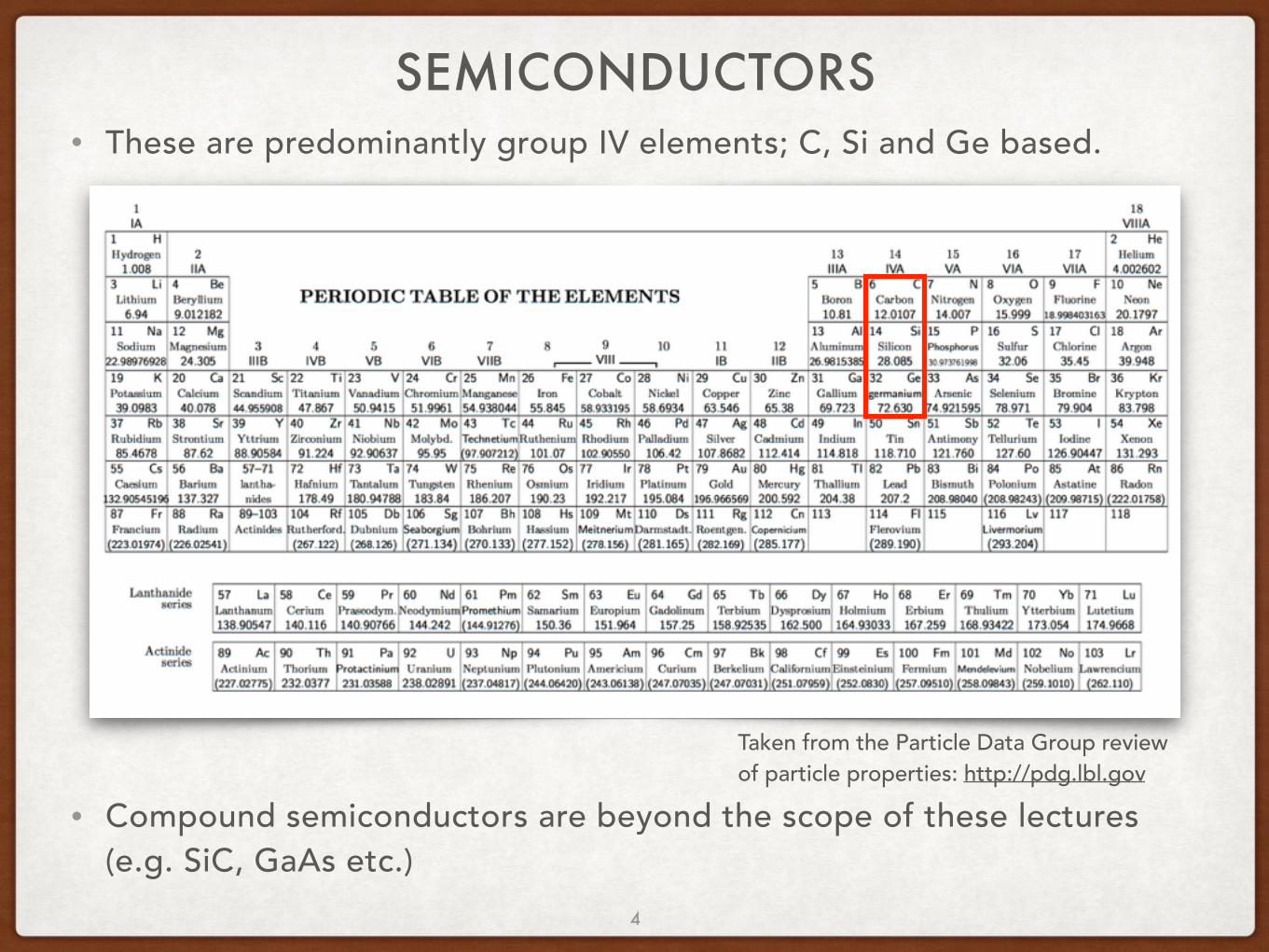
SEMICONDUCTORS• These are predominantly group IV elements; C, Si and Ge based.
• Compound semiconductors are beyond the scope of these lectures (e.g. SiC, GaAs etc.)
Taken from the Particle Data Group review of particle properties: http://pdg.lbl.gov
4
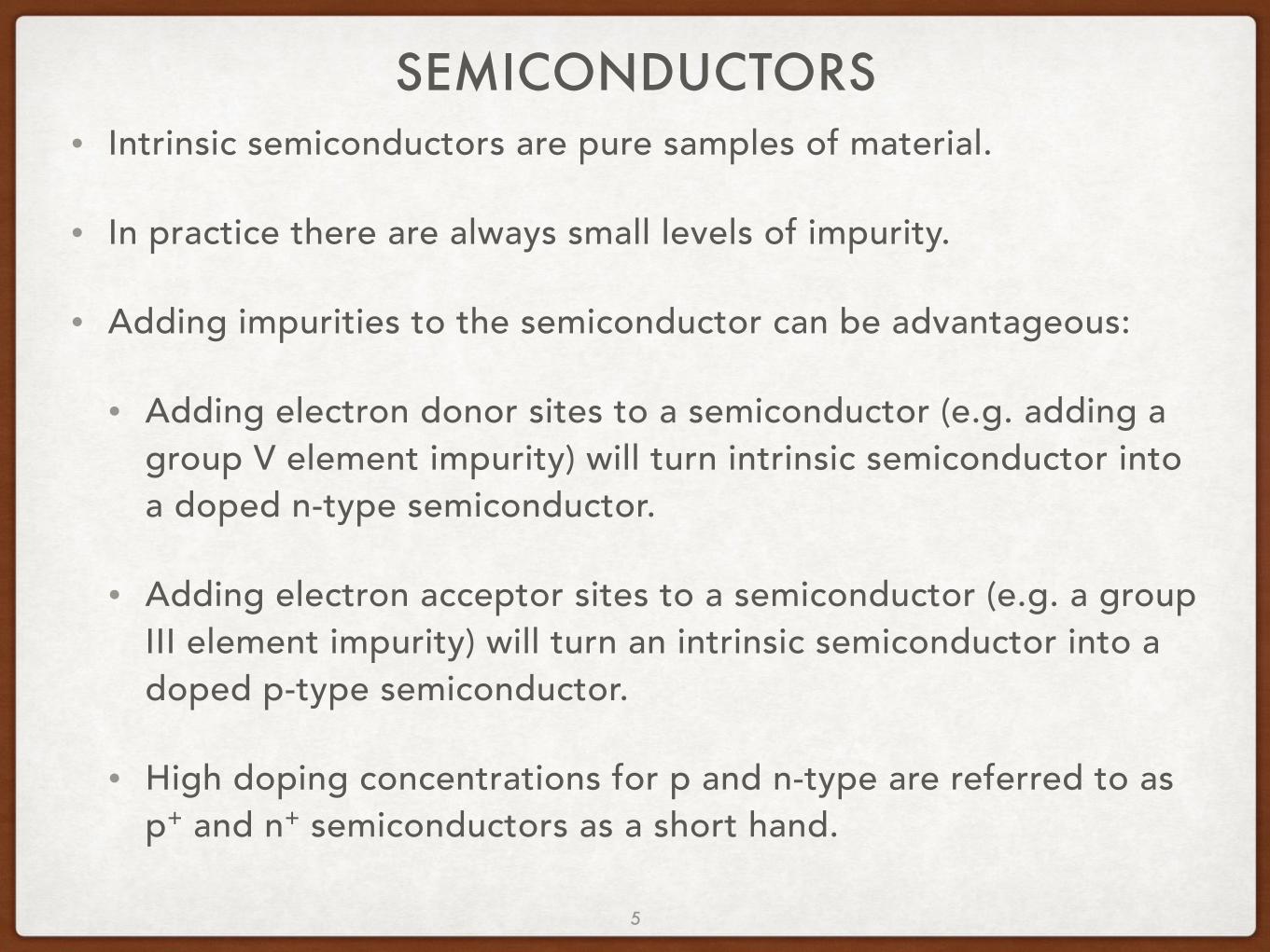
SEMICONDUCTORS• Intrinsic semiconductors are pure samples of material.
• In practice there are always small levels of impurity.
• Adding impurities to the semiconductor can be advantageous:
• Adding electron donor sites to a semiconductor (e.g. adding a group V element impurity) will turn intrinsic semiconductor into a doped n-type semiconductor.
• Adding electron acceptor sites to a semiconductor (e.g. a group III element impurity) will turn an intrinsic semiconductor into a doped p-type semiconductor.
• High doping concentrations for p and n-type are referred to as p+ and n+ semiconductors as a short hand.
5
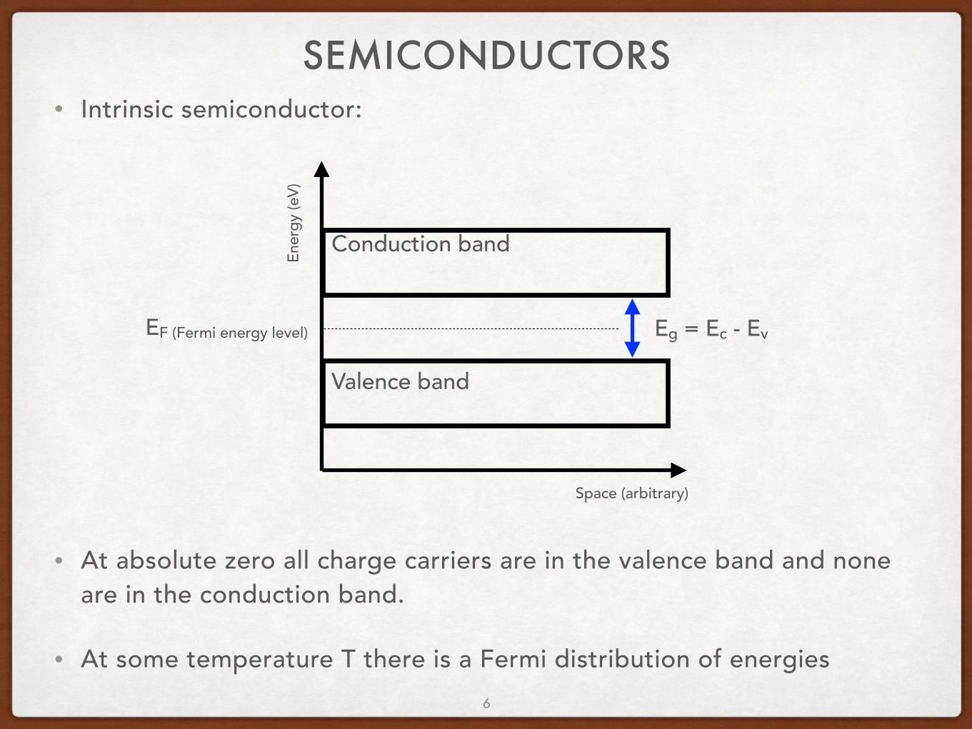
SEMICONDUCTORS• Intrinsic semiconductor:
• At absolute zero all charge carriers are in the valence band and none are in the conduction band.
• At some temperature T there is a Fermi distribution of energies
Valence band
Conduction bandEner
gy (e
V)
Space (arbitrary)
Eg = Ec - EvEF (Fermi energy level)
6

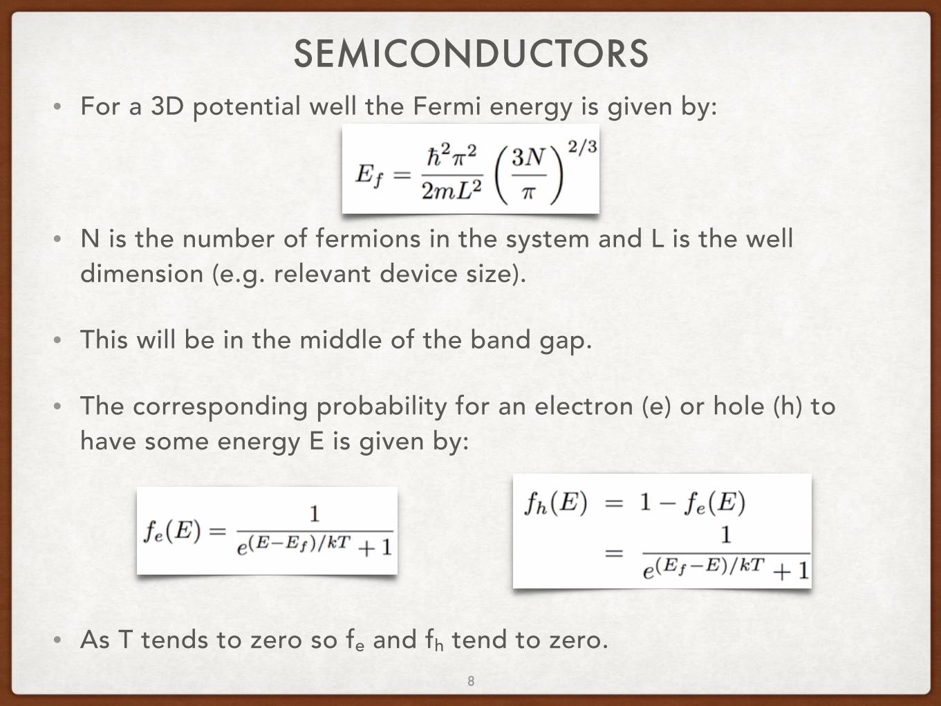
SEMICONDUCTORS• For a 3D potential well the Fermi energy is given by:
• N is the number of fermions in the system and L is the well dimension (e.g. relevant device size).
• This will be in the middle of the band gap.
• The corresponding probability for an electron (e) or hole (h) to have some energy E is given by:
• As T tends to zero so fe and fh tend to zero.8
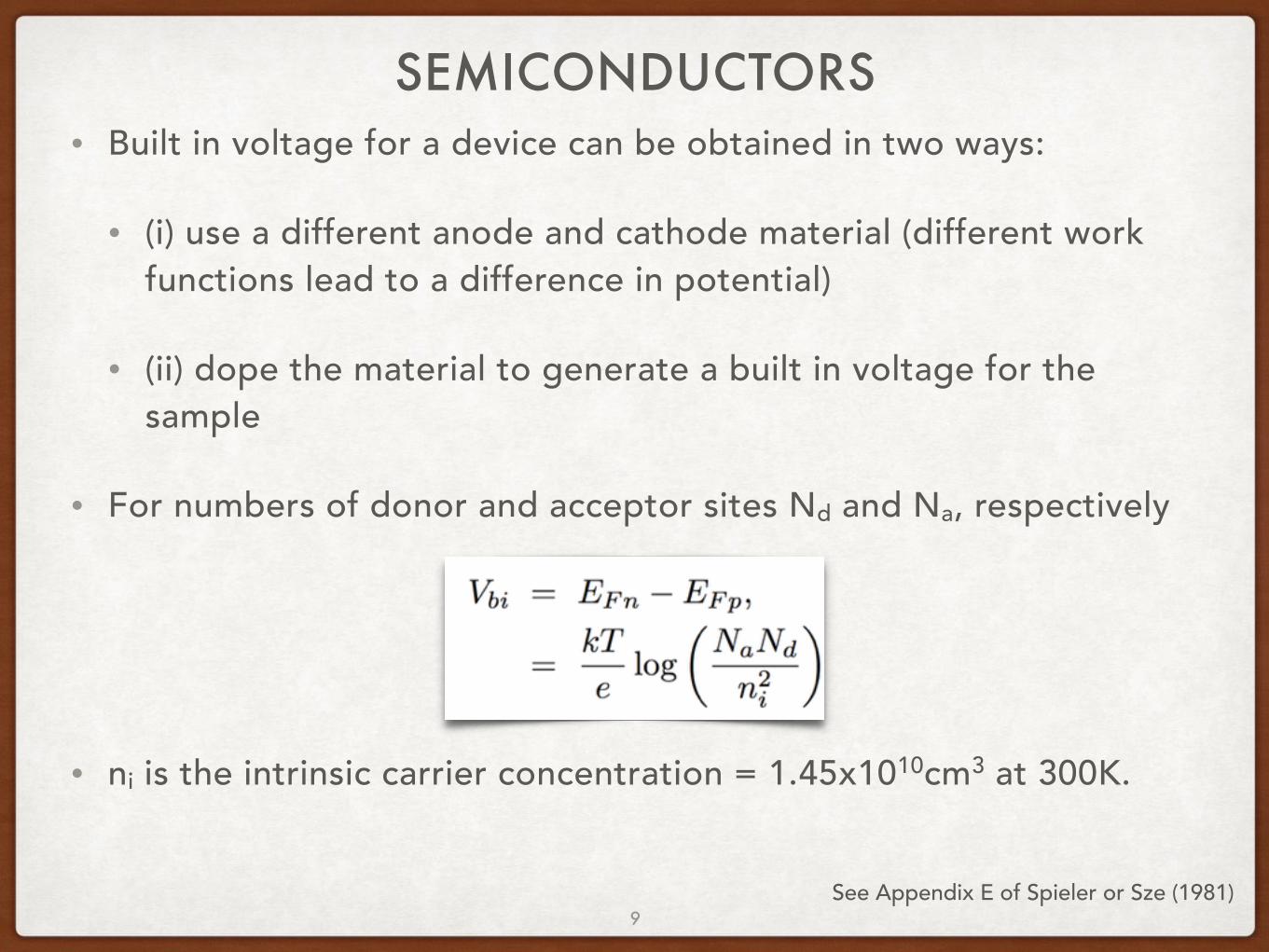
SEMICONDUCTORS• Built in voltage for a device can be obtained in two ways:
• (i) use a different anode and cathode material (different work functions lead to a difference in potential)
• (ii) dope the material to generate a built in voltage for the sample
• For numbers of donor and acceptor sites Nd and Na, respectively
• ni is the intrinsic carrier concentration = 1.45x1010cm3 at 300K.
See Appendix E of Spieler or Sze (1981)9
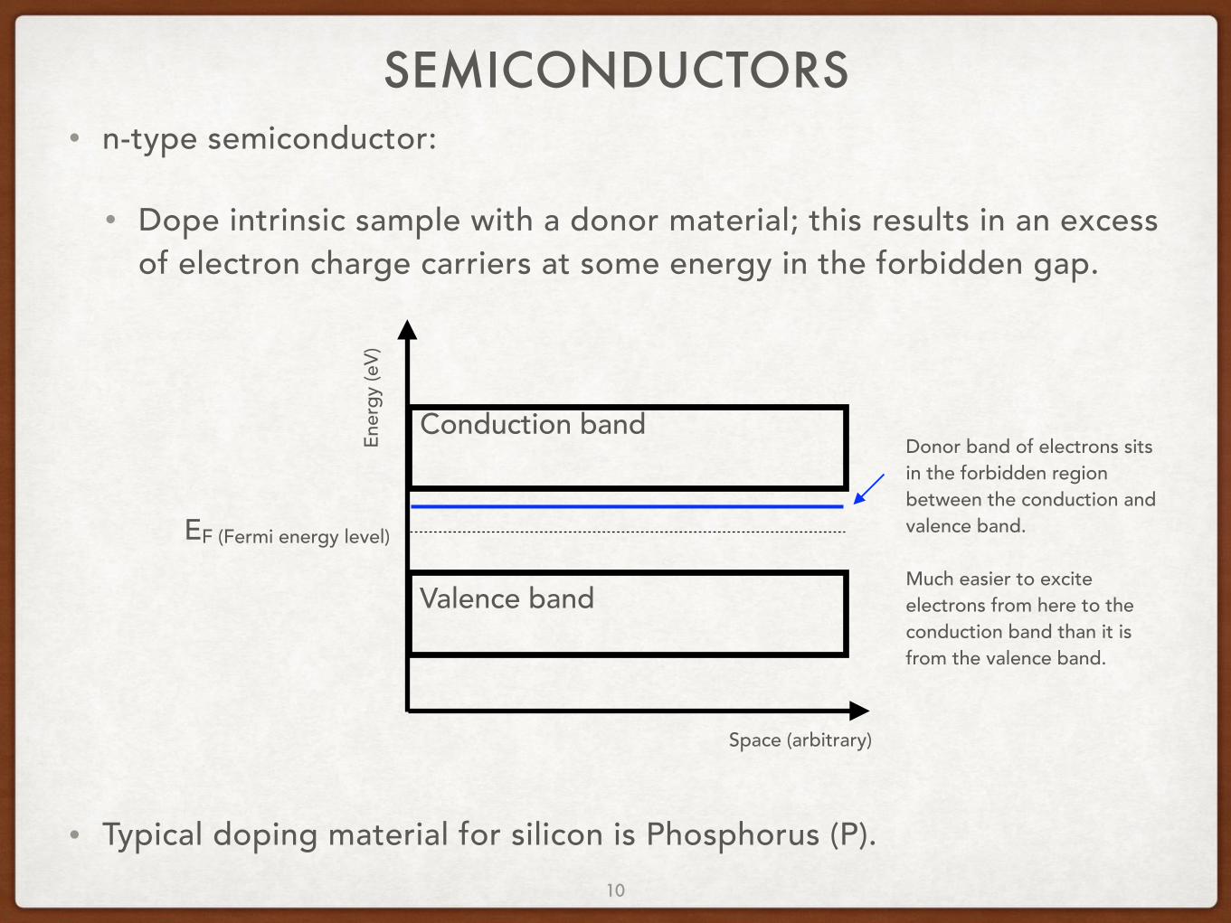
SEMICONDUCTORS• n-type semiconductor:
• Dope intrinsic sample with a donor material; this results in an excess of electron charge carriers at some energy in the forbidden gap.
• Typical doping material for silicon is Phosphorus (P).
Valence band
Conduction bandEner
gy (e
V)
Space (arbitrary)
Donor band of electrons sits in the forbidden region between the conduction and valence band.
Much easier to excite electrons from here to the conduction band than it is from the valence band.
EF (Fermi energy level)
10
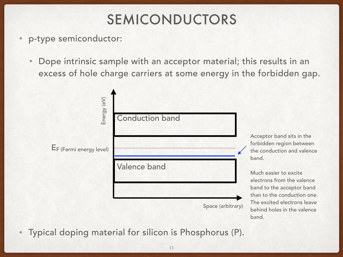
SEMICONDUCTORS• p-type semiconductor:
• Dope intrinsic sample with an acceptor material; this results in an excess of hole charge carriers at some energy in the forbidden gap.
• Typical doping material for silicon is Phosphorus (P).
Valence band
Conduction bandEner
gy (e
V)
Space (arbitrary)
Acceptor band sits in the forbidden region between the conduction and valence band.
Much easier to excite electrons from the valence band to the acceptor band than to the conduction one. The excited electrons leave behind holes in the valence band.
EF (Fermi energy level)
11
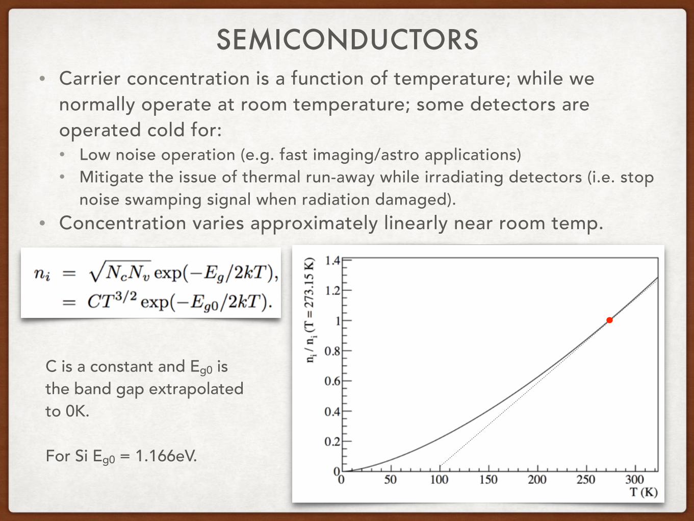
SEMICONDUCTORS• Carrier concentration is a function of temperature; while we
normally operate at room temperature; some detectors are operated cold for: • Low noise operation (e.g. fast imaging/astro applications) • Mitigate the issue of thermal run-away while irradiating detectors (i.e. stop
noise swamping signal when radiation damaged). • Concentration varies approximately linearly near room temp.
C is a constant and Eg0 is the band gap extrapolated to 0K.
For Si Eg0 = 1.166eV.
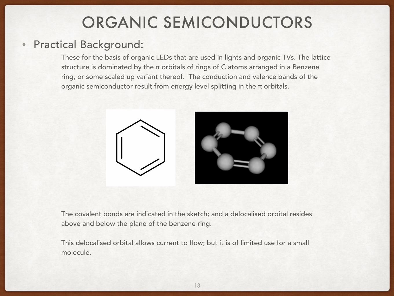
ORGANIC SEMICONDUCTORS• Practical Background:
These for the basis of organic LEDs that are used in lights and organic TVs. The lattice structure is dominated by the π orbitals of rings of C atoms arranged in a Benzene ring, or some scaled up variant thereof. The conduction and valence bands of the organic semiconductor result from energy level splitting in the π orbitals.
The covalent bonds are indicated in the sketch; and a delocalised orbital resides above and below the plane of the benzene ring.
This delocalised orbital allows current to flow; but it is of limited use for a small molecule.
13
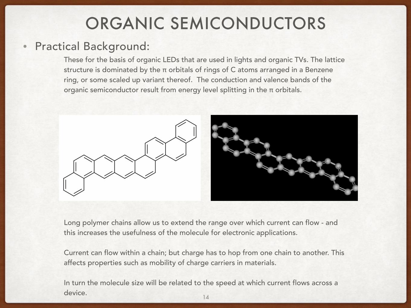
ORGANIC SEMICONDUCTORS• Practical Background:
These for the basis of organic LEDs that are used in lights and organic TVs. The lattice structure is dominated by the π orbitals of rings of C atoms arranged in a Benzene ring, or some scaled up variant thereof. The conduction and valence bands of the organic semiconductor result from energy level splitting in the π orbitals.
Long polymer chains allow us to extend the range over which current can flow - and this increases the usefulness of the molecule for electronic applications.
Current can flow within a chain; but charge has to hop from one chain to another. This affects properties such as mobility of charge carriers in materials.
In turn the molecule size will be related to the speed at which current flows across a device.
14
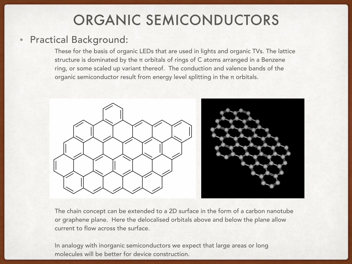
ORGANIC SEMICONDUCTORS• Practical Background:
These for the basis of organic LEDs that are used in lights and organic TVs. The lattice structure is dominated by the π orbitals of rings of C atoms arranged in a Benzene ring, or some scaled up variant thereof. The conduction and valence bands of the organic semiconductor result from energy level splitting in the π orbitals.
The chain concept can be extended to a 2D surface in the form of a carbon nanotube or graphene plane. Here the delocalised orbitals above and below the plane allow current to flow across the surface.
In analogy with inorganic semiconductors we expect that large areas or long molecules will be better for device construction.
INORGANIC SEMICONDUCTORS• Practical Background:
• Silicon devices are fully integrated into our way of life. We rely on these devices for all aspects of our life from appliance control (embedded systems) to fly by wire systems in aeroplanes and everything in-between.
• The simplest type of a semiconductor device is the diode (see next topic). We will use the characteristics of this device in a number of different ways to build detectors.
• A single channel of a semiconductor detector is a reversed biased diode.
• We can process the signal out put from a single channel in order to obtain an analogue or binary signal. There are advantages to analogue information processing V = V(t) vs binary information where V(t) is a sequence of step functions.
16
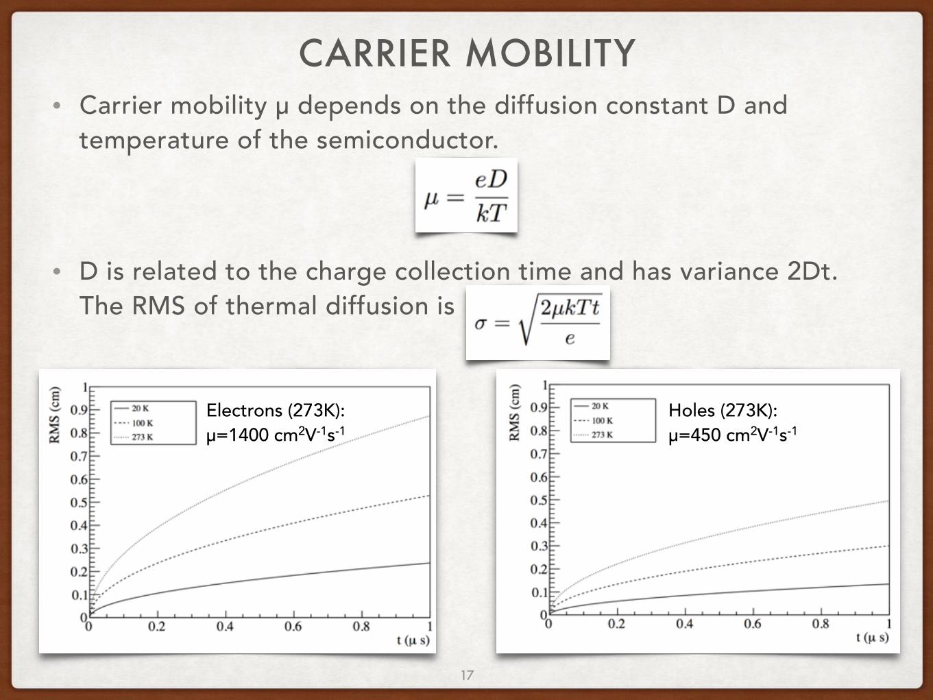
CARRIER MOBILITY• Carrier mobility μ depends on the diffusion constant D and
temperature of the semiconductor.
• D is related to the charge collection time and has variance 2Dt. The RMS of thermal diffusion is
17
Electrons (273K): μ=1400 cm2V-1s-1
Holes (273K): μ=450 cm2V-1s-1
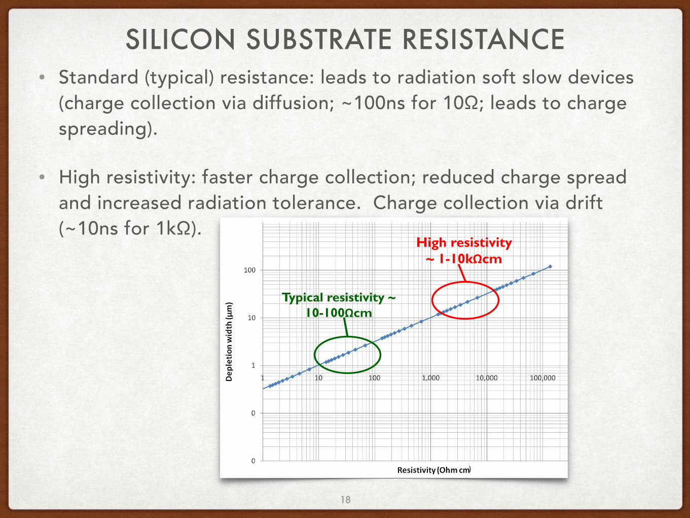
SILICON SUBSTRATE RESISTANCE• Standard (typical) resistance: leads to radiation soft slow devices
(charge collection via diffusion; ~100ns for 10Ω; leads to charge spreading).
• High resistivity: faster charge collection; reduced charge spread and increased radiation tolerance. Charge collection via drift (~10ns for 1kΩ).
)
Typical resistivity ~ 10-100Ωcm
High resistivity ~ 1-10kΩcm
18
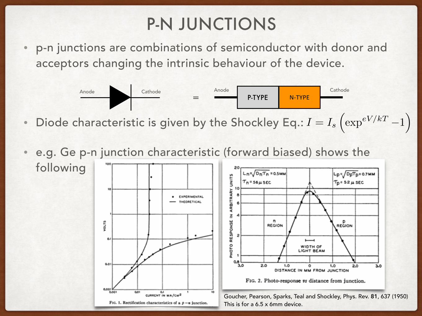
P-N JUNCTIONS• p-n junctions are combinations of semiconductor with donor and
acceptors changing the intrinsic behaviour of the device.
• Diode characteristic is given by the Shockley Eq.:
• e.g. Ge p-n junction characteristic (forward biased) shows the following
19
Anode Cathode = P-TYPE N-TYPEAnode Cathode
I = Is⇣exp
eV/kT �1
⌘
Goucher, Pearson, Sparks, Teal and Shockley, Phys. Rev. 81, 637 (1950) This is for a 6.5 x 6mm device.
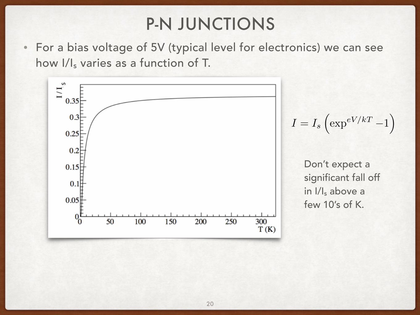
P-N JUNCTIONS• For a bias voltage of 5V (typical level for electronics) we can see
how I/Is varies as a function of T.
I = Is⇣exp
eV/kT �1
⌘
S
Don’t expect a significant fall off in I/Is above a few 10’s of K.
20
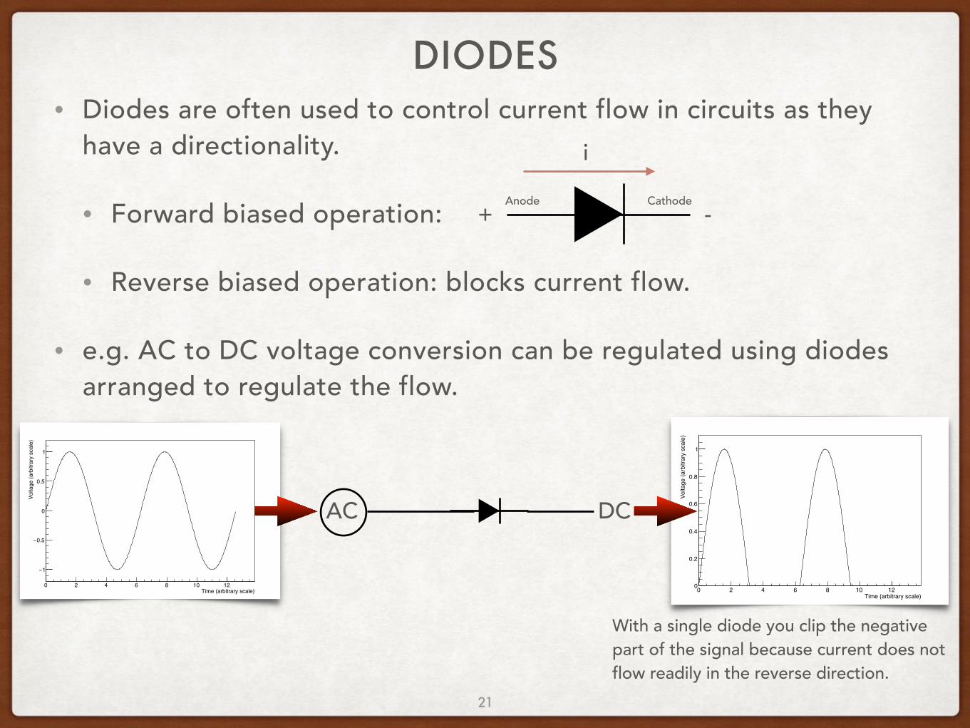
DIODES• Diodes are often used to control current flow in circuits as they
have a directionality.
• Forward biased operation:
• Reverse biased operation: blocks current flow.
• e.g. AC to DC voltage conversion can be regulated using diodes arranged to regulate the flow.
Anode Cathode+ -
i
AC DC
Time (arbitrary scale)0 2 4 6 8 10 12
Volta
ge (a
rbitr
ary
scal
e)
1−
0.5−
0
0.5
1
Time (arbitrary scale)0 2 4 6 8 10 12
Volta
ge (a
rbitr
ary
scal
e)
0
0.2
0.4
0.6
0.8
1
With a single diode you clip the negative part of the signal because current does not flow readily in the reverse direction.
21
Time (arbitrary scale)0 2 4 6 8 10 12
Volta
ge (a
rbitr
ary
scal
e)
0
0.2
0.4
0.6
0.8
1
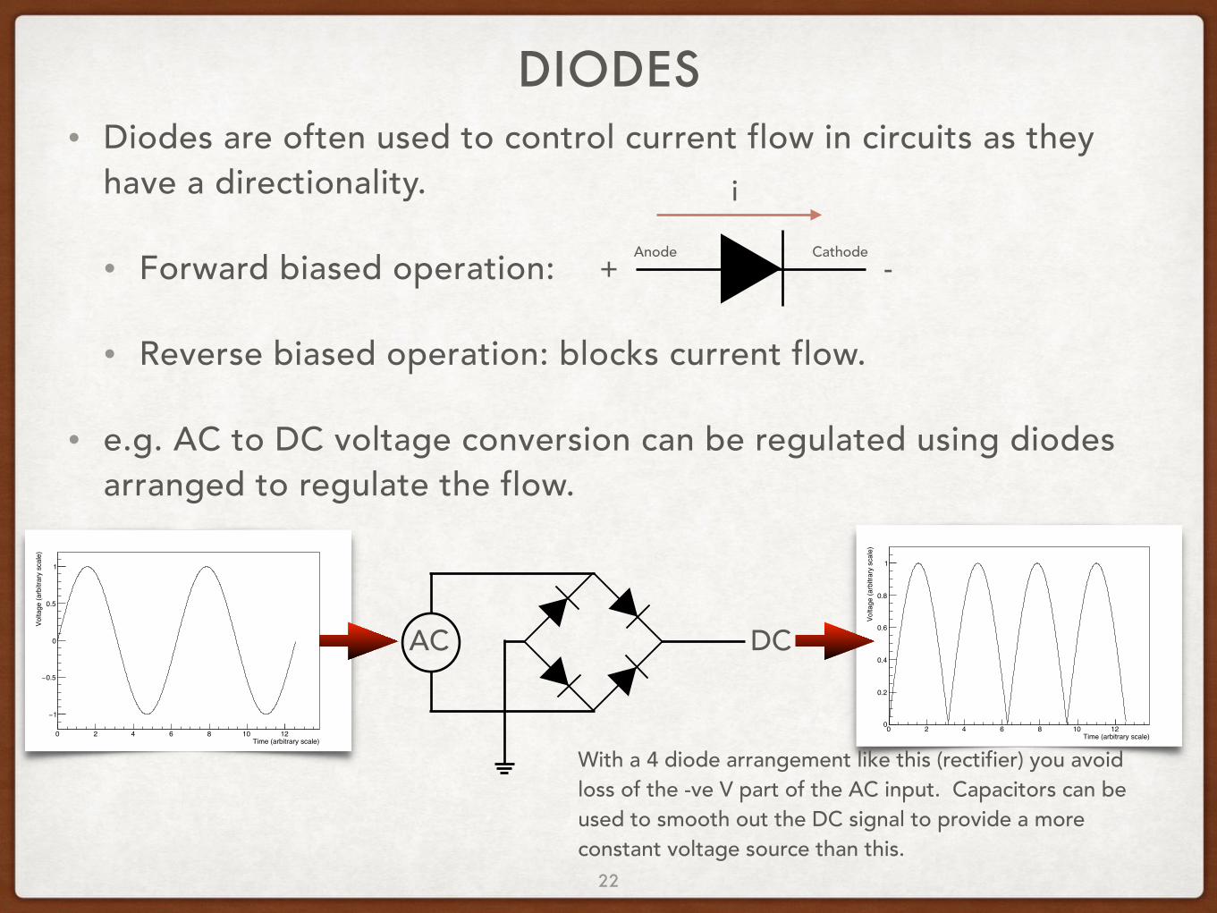
DIODES• Diodes are often used to control current flow in circuits as they
have a directionality.
• Forward biased operation:
• Reverse biased operation: blocks current flow.
• e.g. AC to DC voltage conversion can be regulated using diodes arranged to regulate the flow.
Anode Cathode+ -
i
AC DC
Time (arbitrary scale)0 2 4 6 8 10 12
Volta
ge (a
rbitr
ary
scal
e)
1−
0.5−
0
0.5
1
With a 4 diode arrangement like this (rectifier) you avoid loss of the -ve V part of the AC input. Capacitors can be used to smooth out the DC signal to provide a more constant voltage source than this.
22
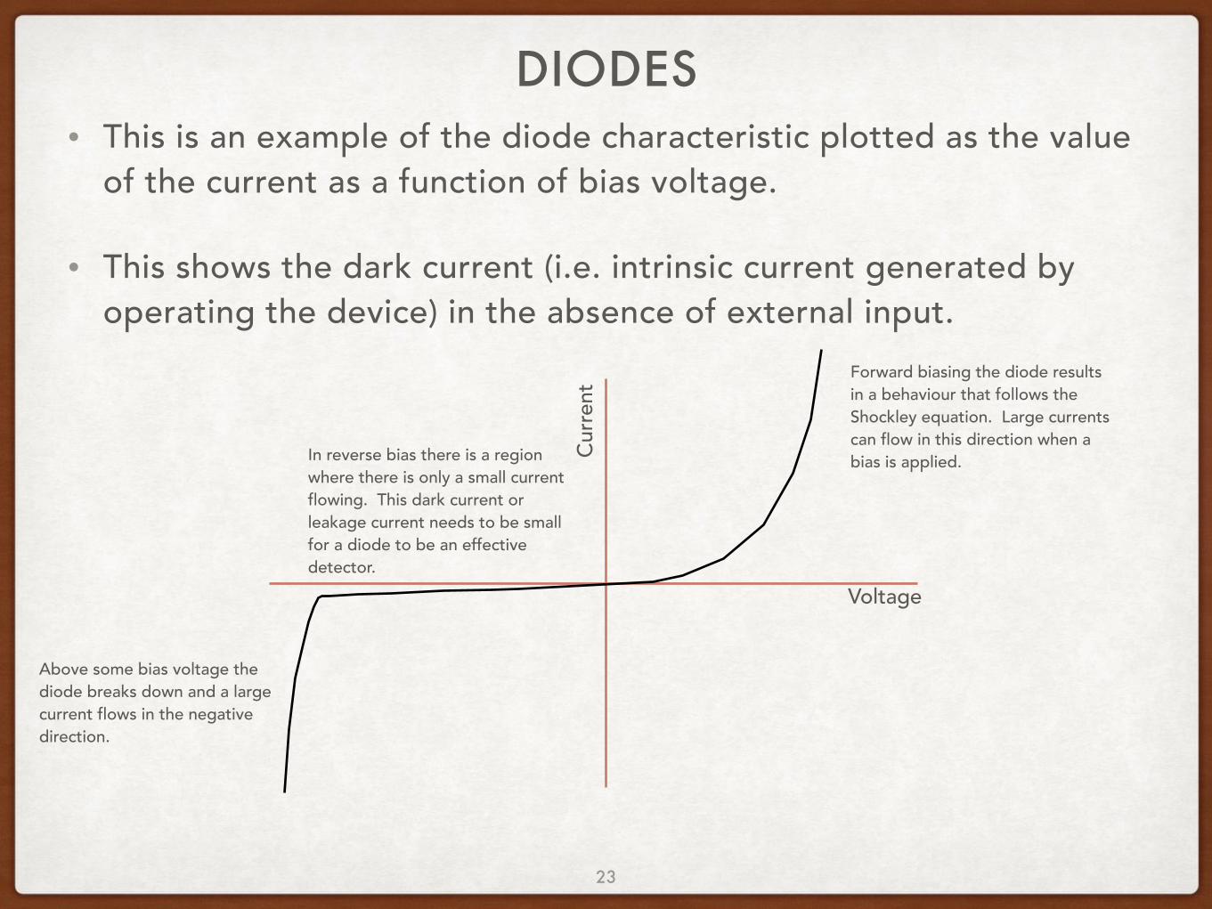
DIODES• This is an example of the diode characteristic plotted as the value
of the current as a function of bias voltage.
• This shows the dark current (i.e. intrinsic current generated by operating the device) in the absence of external input.
23
VoltageCu
rrent
Forward biasing the diode results in a behaviour that follows the Shockley equation. Large currents can flow in this direction when a bias is applied.In reverse bias there is a region
where there is only a small current flowing. This dark current or leakage current needs to be small for a diode to be an effective detector.
Above some bias voltage the diode breaks down and a large current flows in the negative direction.
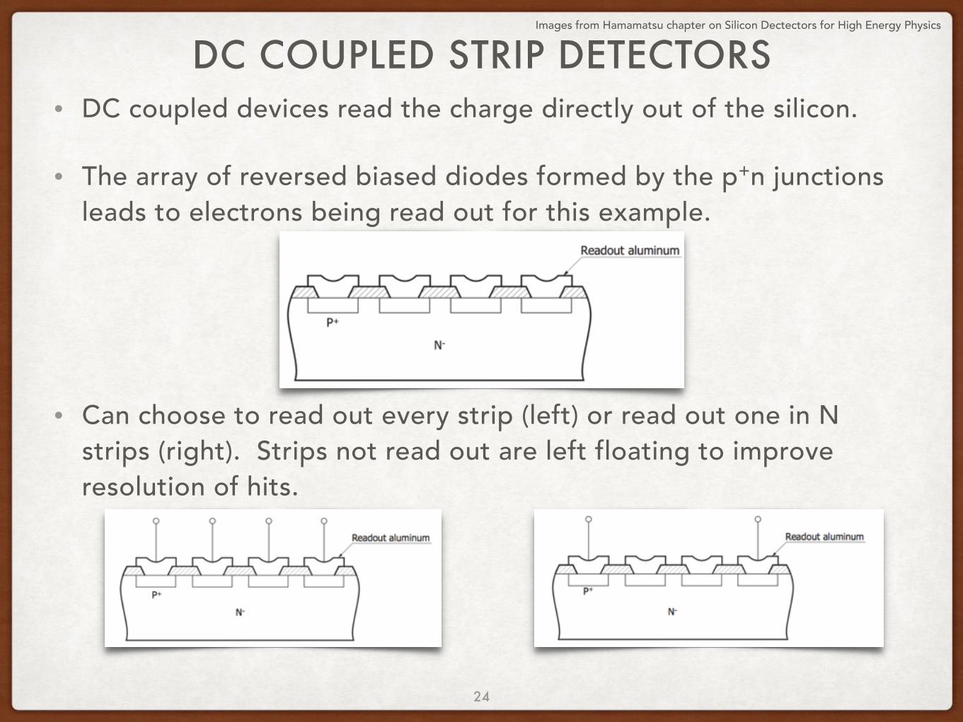
DC COUPLED STRIP DETECTORS• DC coupled devices read the charge directly out of the silicon.
• The array of reversed biased diodes formed by the p+n junctions leads to electrons being read out for this example.
• Can choose to read out every strip (left) or read out one in N strips (right). Strips not read out are left floating to improve resolution of hits.
Images from Hamamatsu chapter on Silicon Dectectors for High Energy Physics
24
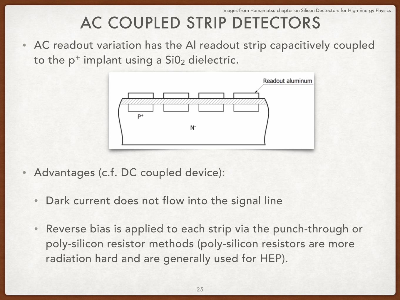
AC COUPLED STRIP DETECTORS• AC readout variation has the Al readout strip capacitively coupled
to the p+ implant using a Si02 dielectric.
• Advantages (c.f. DC coupled device):
• Dark current does not flow into the signal line
• Reverse bias is applied to each strip via the punch-through or poly-silicon resistor methods (poly-silicon resistors are more radiation hard and are generally used for HEP).
Images from Hamamatsu chapter on Silicon Dectectors for High Energy Physics
25
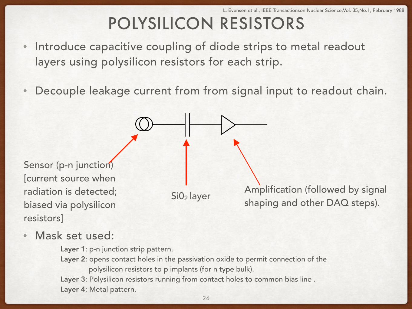
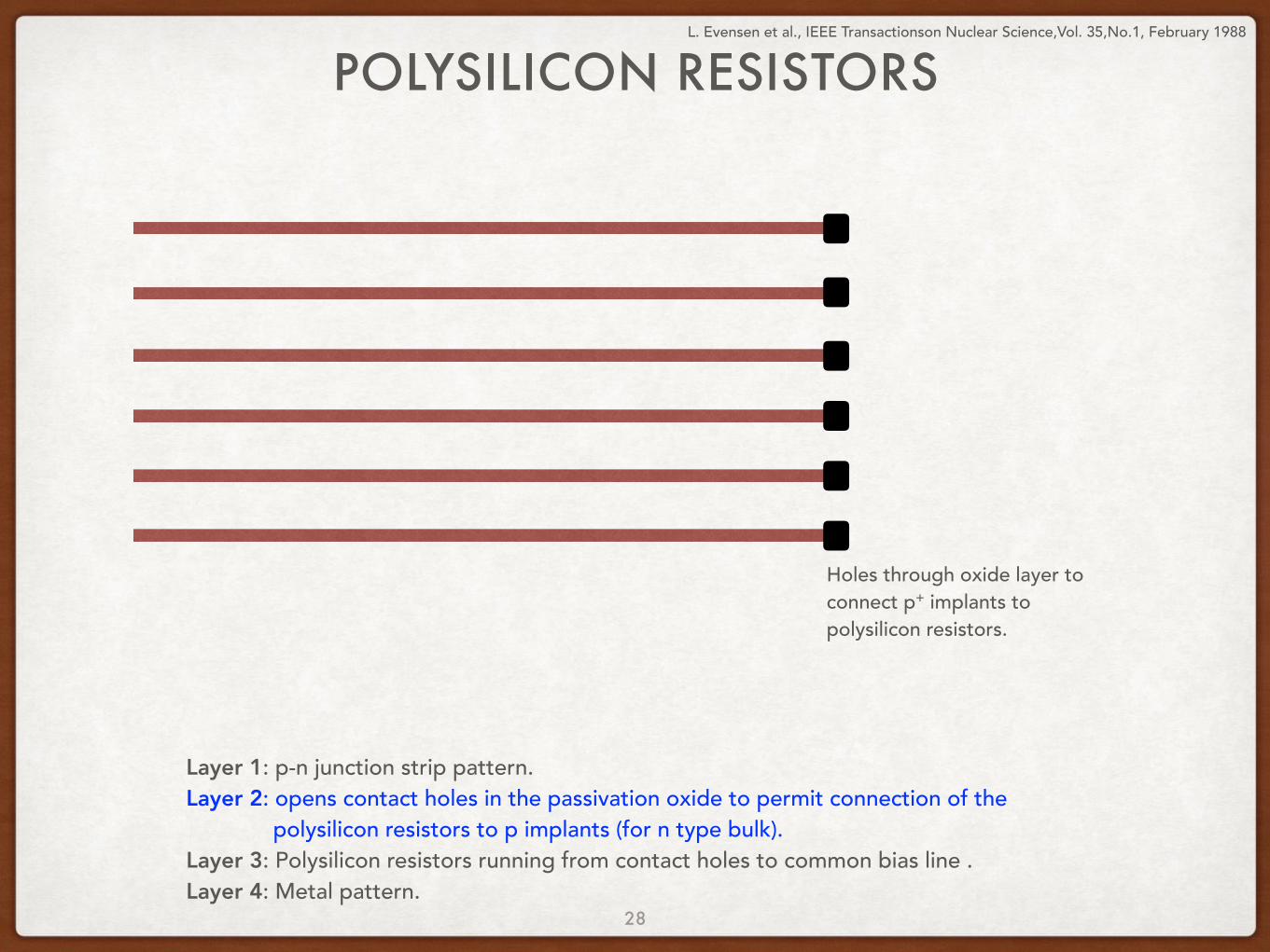
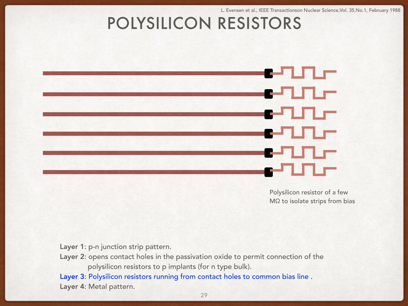
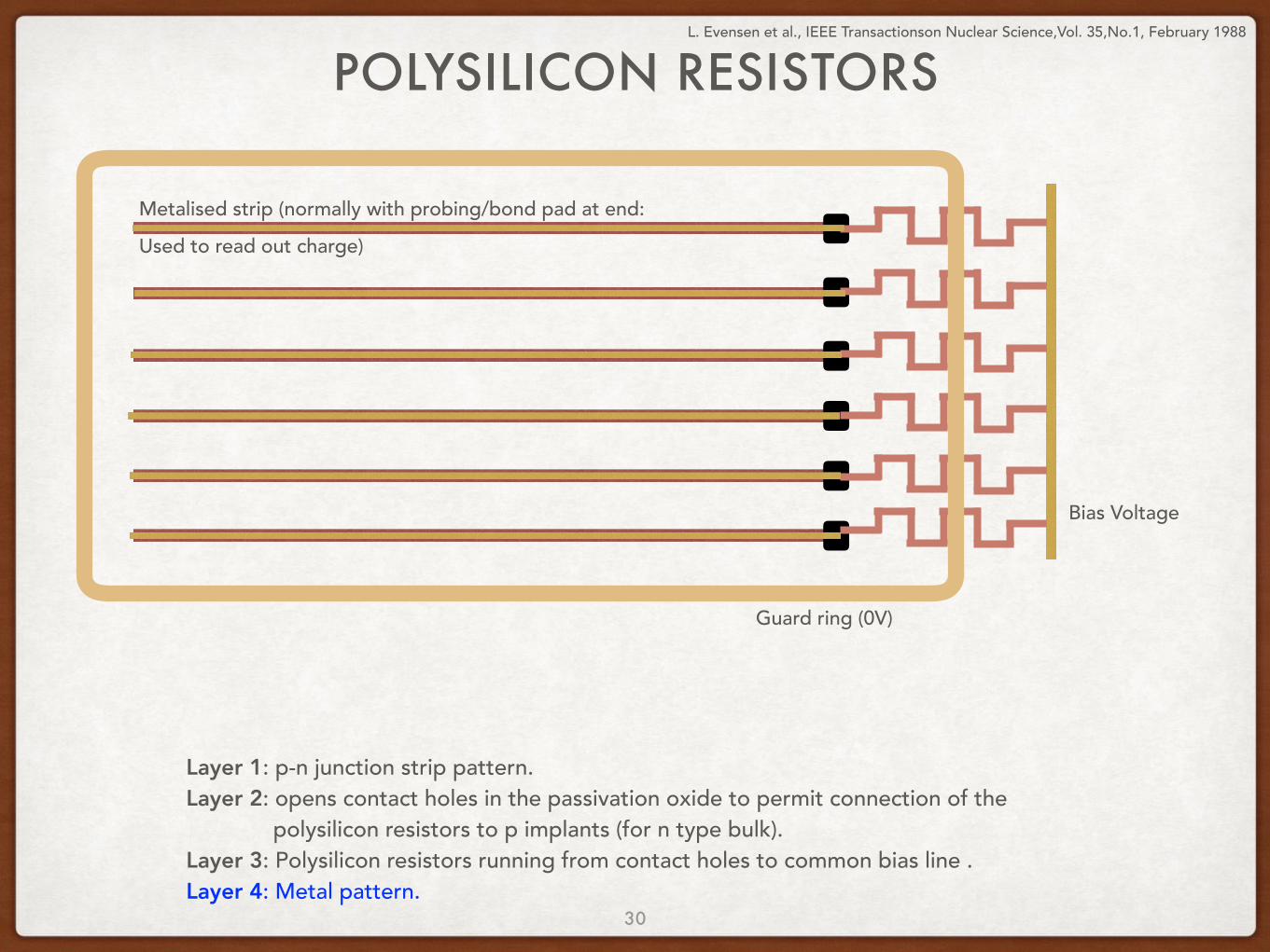
POLYSILICON RESISTORS• Introduce capacitive coupling of diode strips to metal readout
layers using polysilicon resistors for each strip.
• Decouple leakage current from from signal input to readout chain.
• Mask set used:
L. Evensen et al., IEEE Transactionson Nuclear Science,Vol. 35,No.1, February 1988
Sensor (p-n junction) [current source when radiation is detected; biased via polysilicon resistors]
Si02 layer Amplification (followed by signal shaping and other DAQ steps).
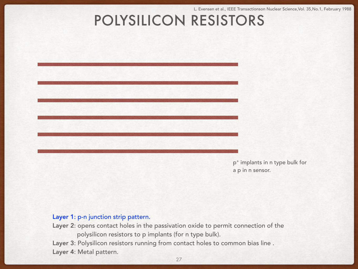
Layer 1: p-n junction strip pattern. Layer 2: opens contact holes in the passivation oxide to permit connection of the polysilicon resistors to p implants (for n type bulk). Layer 3: Polysilicon resistors running from contact holes to common bias line . Layer 4: Metal pattern.
26
POLYSILICON RESISTORSL. Evensen et al., IEEE Transactionson Nuclear Science,Vol. 35,No.1, February 1988
Layer 1: p-n junction strip pattern. Layer 2: opens contact holes in the passivation oxide to permit connection of the polysilicon resistors to p implants (for n type bulk). Layer 3: Polysilicon resistors running from contact holes to common bias line . Layer 4: Metal pattern.
p+ implants in n type bulk for a p in n sensor.
27
POLYSILICON RESISTORSL. Evensen et al., IEEE Transactionson Nuclear Science,Vol. 35,No.1, February 1988
Layer 1: p-n junction strip pattern. Layer 2: opens contact holes in the passivation oxide to permit connection of the polysilicon resistors to p implants (for n type bulk). Layer 3: Polysilicon resistors running from contact holes to common bias line . Layer 4: Metal pattern.
Holes through oxide layer to connect p+ implants to polysilicon resistors.
28
POLYSILICON RESISTORSL. Evensen et al., IEEE Transactionson Nuclear Science,Vol. 35,No.1, February 1988
Layer 1: p-n junction strip pattern. Layer 2: opens contact holes in the passivation oxide to permit connection of the polysilicon resistors to p implants (for n type bulk). Layer 3: Polysilicon resistors running from contact holes to common bias line . Layer 4: Metal pattern.
Polysilicon resistor of a few MΩ to isolate strips from bias
29
POLYSILICON RESISTORSL. Evensen et al., IEEE Transactionson Nuclear Science,Vol. 35,No.1, February 1988
Layer 1: p-n junction strip pattern. Layer 2: opens contact holes in the passivation oxide to permit connection of the polysilicon resistors to p implants (for n type bulk). Layer 3: Polysilicon resistors running from contact holes to common bias line . Layer 4: Metal pattern.
Guard ring (0V)
Bias Voltage
Metalised strip (normally with probing/bond pad at end: Used to read out charge)
30
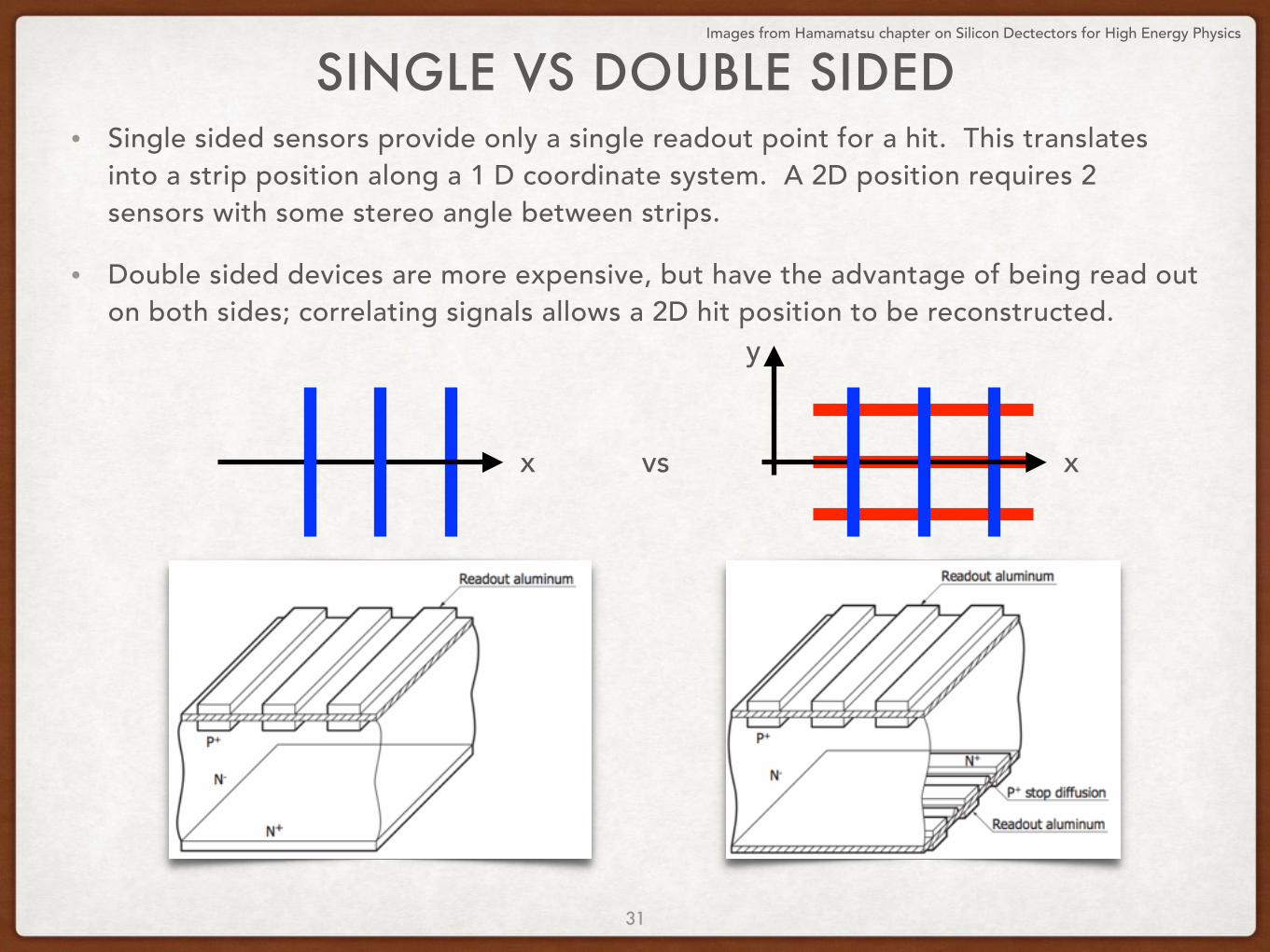
SINGLE VS DOUBLE SIDED• Single sided sensors provide only a single readout point for a hit. This translates
into a strip position along a 1 D coordinate system. A 2D position requires 2 sensors with some stereo angle between strips.
• Double sided devices are more expensive, but have the advantage of being read out on both sides; correlating signals allows a 2D hit position to be reconstructed.
Images from Hamamatsu chapter on Silicon Dectectors for High Energy Physics
x vs x
y
31
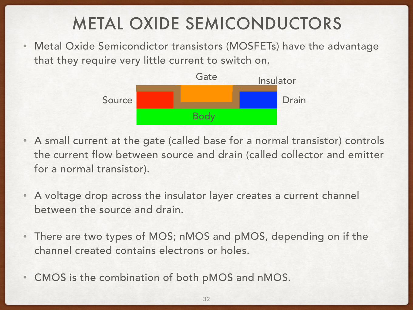
METAL OXIDE SEMICONDUCTORS• Metal Oxide Semicondictor transistors (MOSFETs) have the advantage
that they require very little current to switch on.
• A small current at the gate (called base for a normal transistor) controls the current flow between source and drain (called collector and emitter for a normal transistor).
• A voltage drop across the insulator layer creates a current channel between the source and drain.
• There are two types of MOS; nMOS and pMOS, depending on if the channel created contains electrons or holes.
• CMOS is the combination of both pMOS and nMOS.32
Source DrainBody
Gate Insulator
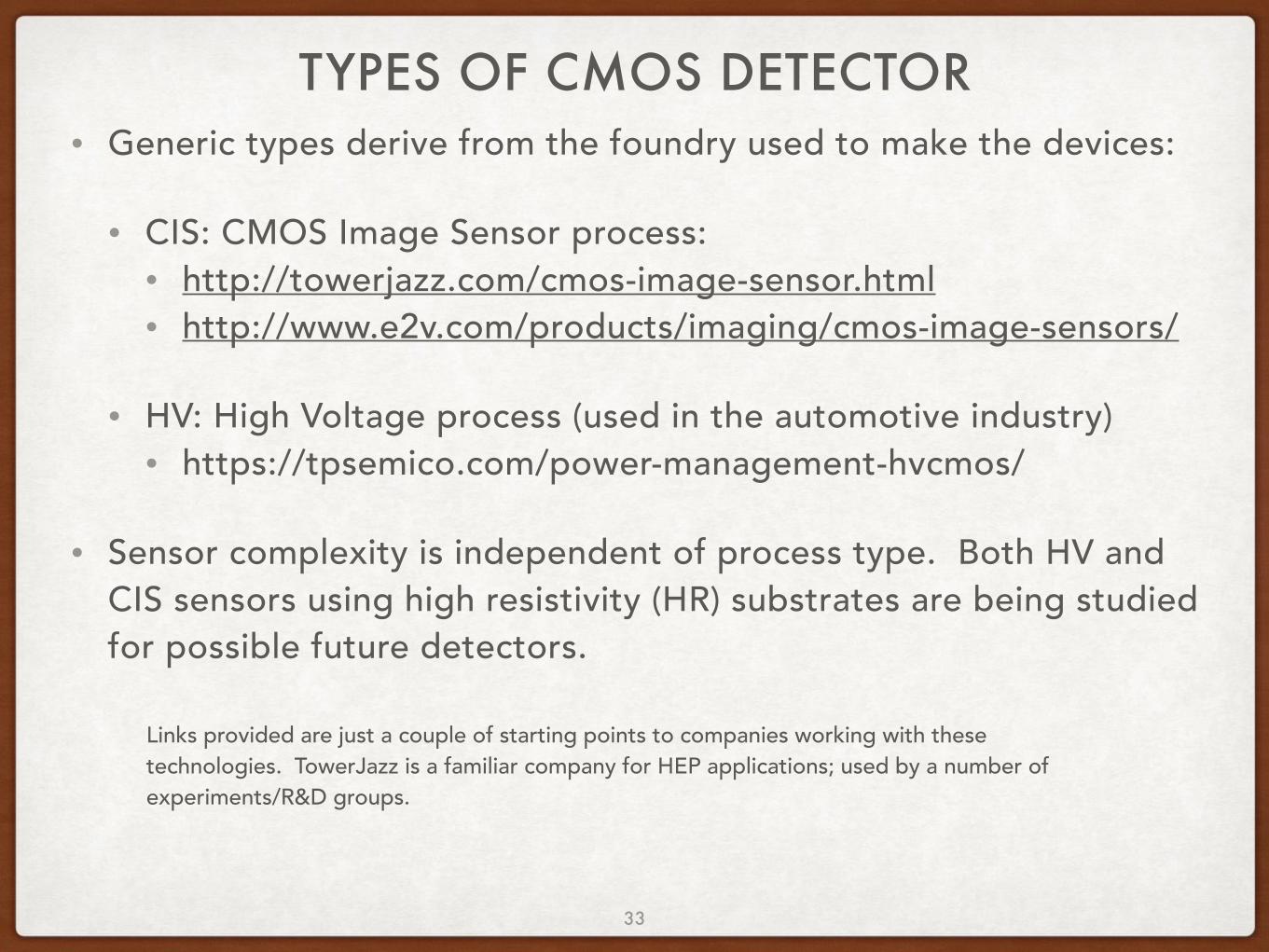
TYPES OF CMOS DETECTOR• Generic types derive from the foundry used to make the devices:
• CIS: CMOS Image Sensor process: • http://towerjazz.com/cmos-image-sensor.html • http://www.e2v.com/products/imaging/cmos-image-sensors/
• HV: High Voltage process (used in the automotive industry) • https://tpsemico.com/power-management-hvcmos/
• Sensor complexity is independent of process type. Both HV and CIS sensors using high resistivity (HR) substrates are being studied for possible future detectors.
33
Links provided are just a couple of starting points to companies working with these technologies. TowerJazz is a familiar company for HEP applications; used by a number of experiments/R&D groups.
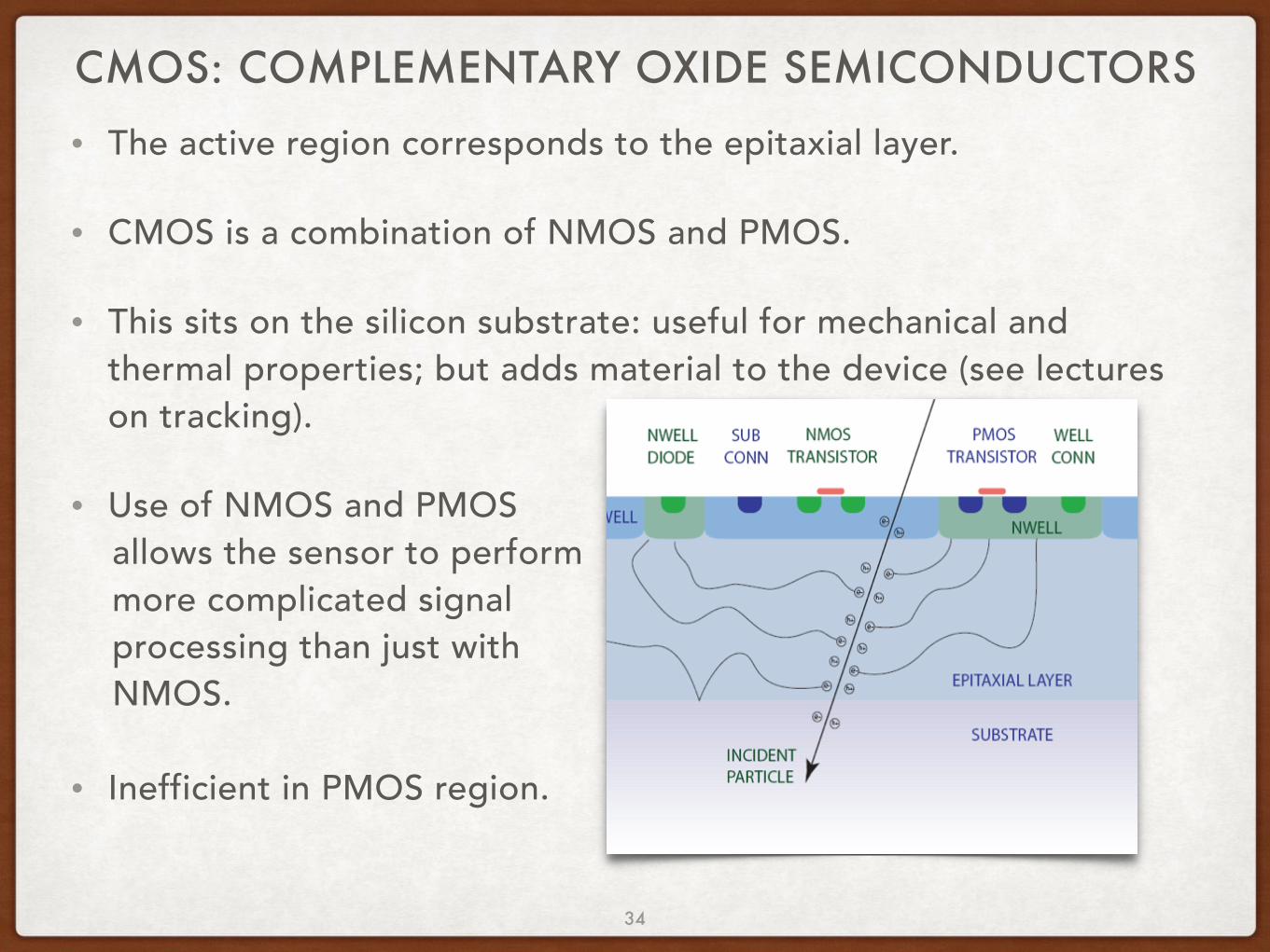
CMOS: COMPLEMENTARY OXIDE SEMICONDUCTORS• The active region corresponds to the epitaxial layer.
• CMOS is a combination of NMOS and PMOS.
• This sits on the silicon substrate: useful for mechanical and thermal properties; but adds material to the device (see lectures on tracking).
• Use of NMOS and PMOS allows the sensor to perform more complicated signal processing than just with NMOS.
• Inefficient in PMOS region.
34
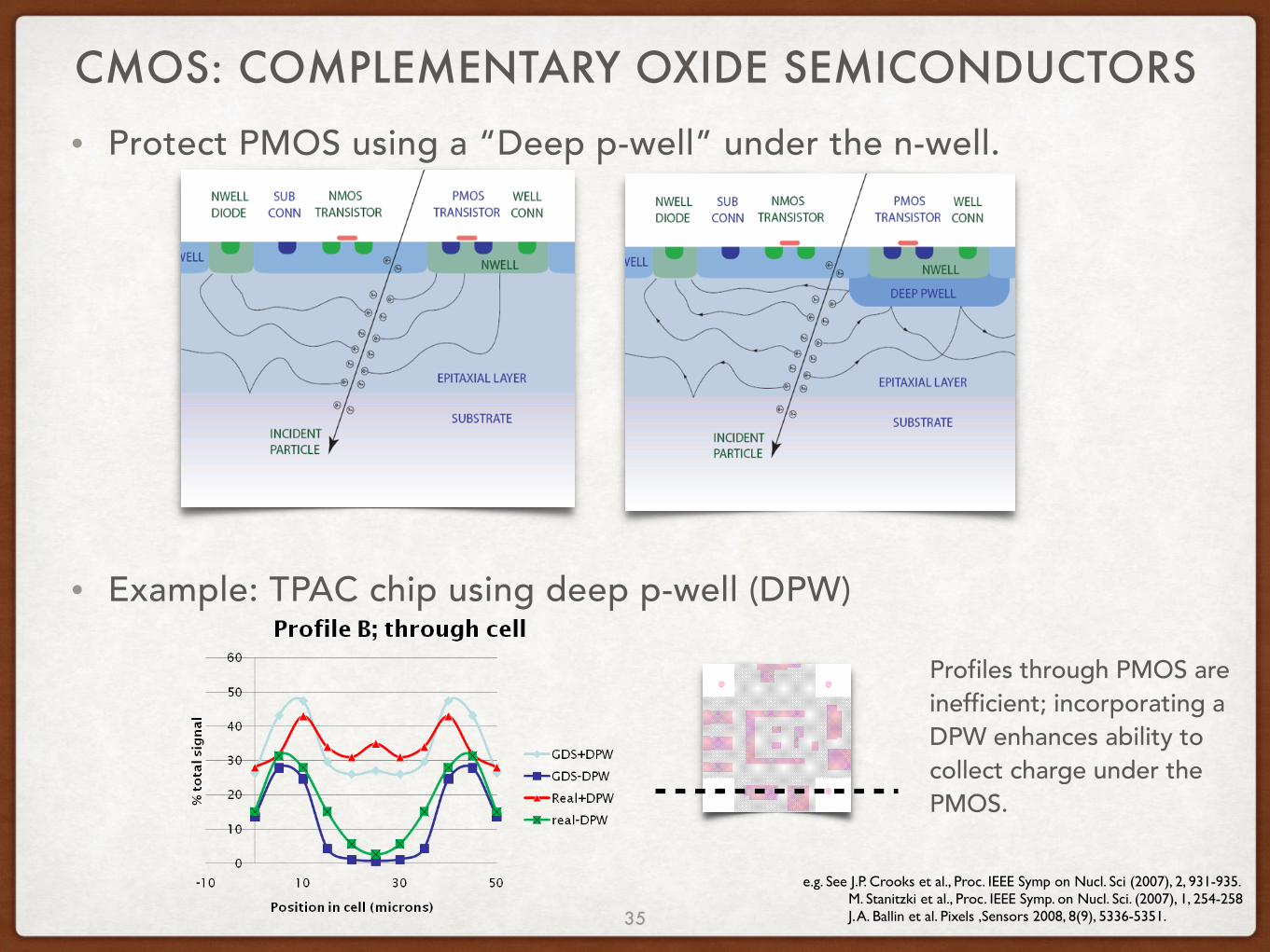
CMOS: COMPLEMENTARY OXIDE SEMICONDUCTORS• Protect PMOS using a “Deep p-well” under the n-well.
• Example: TPAC chip using deep p-well (DPW)
e.g. See J.P. Crooks et al., Proc. IEEE Symp on Nucl. Sci (2007), 2, 931-935. M. Stanitzki et al., Proc. IEEE Symp. on Nucl. Sci. (2007), 1, 254-258 J. A. Ballin et al. Pixels ,Sensors 2008, 8(9), 5336-5351.
Profiles through PMOS are inefficient; incorporating a DPW enhances ability to collect charge under the PMOS.
35
CMOS: COMPLEMENTARY OXIDE SEMICONDUCTORS• Advantages of CMOS over other types of radiation detector:
• Can be very thin; low mass is good for tracking particles.
• Can be cheap; use commercial processes / adaptations of commercial processes, so are a small consumer that uses technology as opposed to driving development.
• Potential disadvantages:
• Not widely used (yet); so limitations are unclear.
• Some test beam structures and telescopes use CMOS. The STAR tracker uses CMOS and the ALICE ITS will use CMOS.
• It is an interesting technology that a lot of people are working with to learn more.
http://www-rnc.lbl.gov/STAR/conf/talks2000/wieman.pdf http://inspirehep.net/record/1354936/files/10.1088_1748-0221_10_03_C03030.pdf?version=1
36
RADIATION DETECTION• Different types of radiation interact differently with matter.
• Photons:• Photons will pass undetected through material up until the point where they
interact. At that point the quantum of energy will be converted into something detectable. Understanding methods of interaction for a given application is an important input to device design.
• Photon detectors are detected at a photocathode; where the mechanism of photo-conduction is used in order to convert the γ to an electron. That electron is subsequently accelerated in order to produce a large enough signal for detection.
• Another mechanism for photon detection is photon conversion to e+e— pairs in the presence of materials; i.e.
� ! e+e�
37
See Knoll, Ch 2. Particle Data Group, Review of Particle Physics note on “Passage of particles through matter” http://pdg.lbl.gov/2015/reviews/rpp2015-rev-passage-particles-matter.pdf
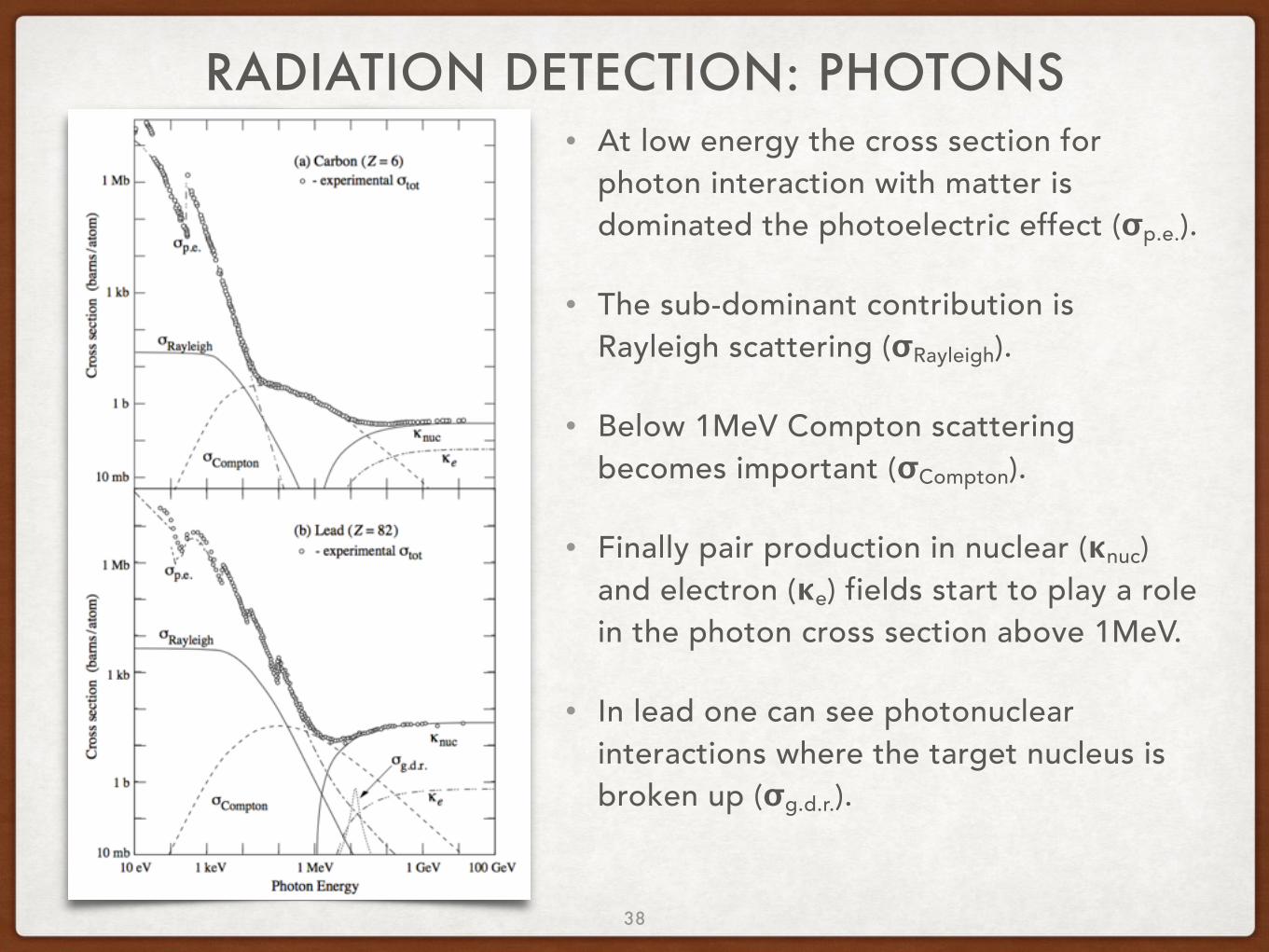
RADIATION DETECTION: PHOTONS• At low energy the cross section for
photon interaction with matter is dominated the photoelectric effect (σp.e.).
• The sub-dominant contribution is Rayleigh scattering (σRayleigh).
• Below 1MeV Compton scattering becomes important (σCompton).
• Finally pair production in nuclear (κnuc) and electron (κe) fields start to play a role in the photon cross section above 1MeV.
• In lead one can see photonuclear interactions where the target nucleus is broken up (σg.d.r.).
38
RADIATION DETECTION: PHOTONS
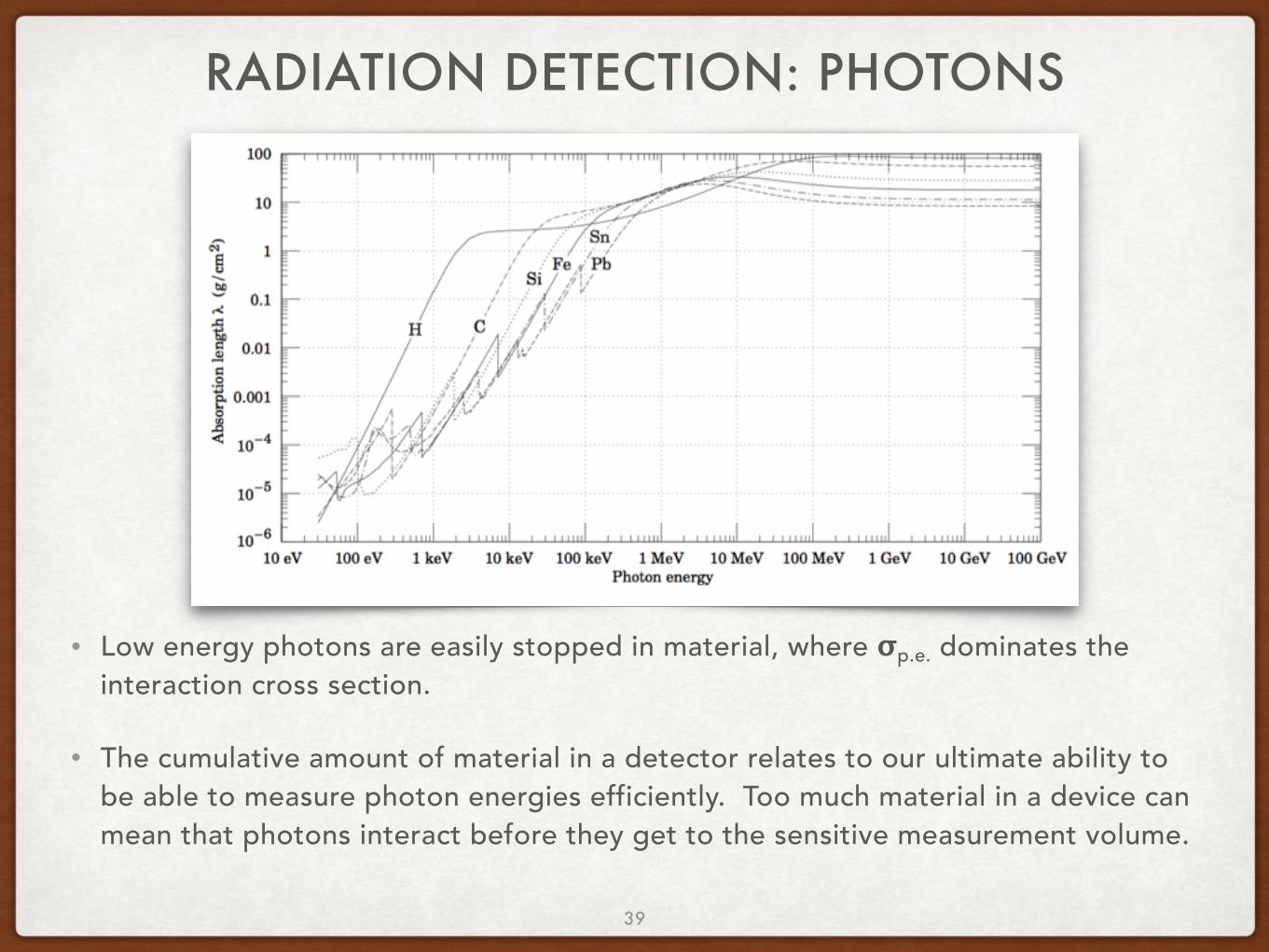
• Low energy photons are easily stopped in material, where σp.e. dominates the interaction cross section.
• The cumulative amount of material in a detector relates to our ultimate ability to be able to measure photon energies efficiently. Too much material in a device can mean that photons interact before they get to the sensitive measurement volume.
39
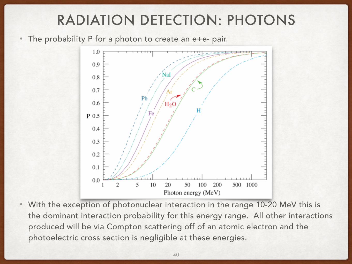
RADIATION DETECTION: PHOTONS• The probability P for a photon to create an e+e- pair.
• With the exception of photonuclear interaction in the range 10-20 MeV this is the dominant interaction probability for this energy range. All other interactions produced will be via Compton scattering off of an atomic electron and the photoelectric cross section is negligible at these energies.
40
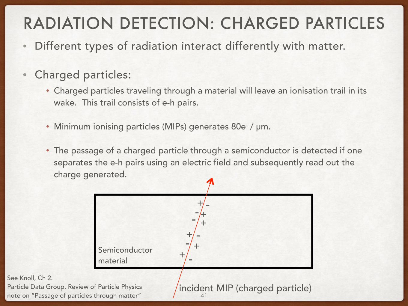
RADIATION DETECTION: CHARGED PARTICLES• Different types of radiation interact differently with matter.
• Charged particles:• Charged particles traveling through a material will leave an ionisation trail in its
wake. This trail consists of e-h pairs.
• Minimum ionising particles (MIPs) generates 80e- / μm.
• The passage of a charged particle through a semiconductor is detected if one separates the e-h pairs using an electric field and subsequently read out the charge generated.
+++
++
+ -- --
--
Semiconductor material
incident MIP (charged particle)41
See Knoll, Ch 2. Particle Data Group, Review of Particle Physics note on “Passage of particles through matter”
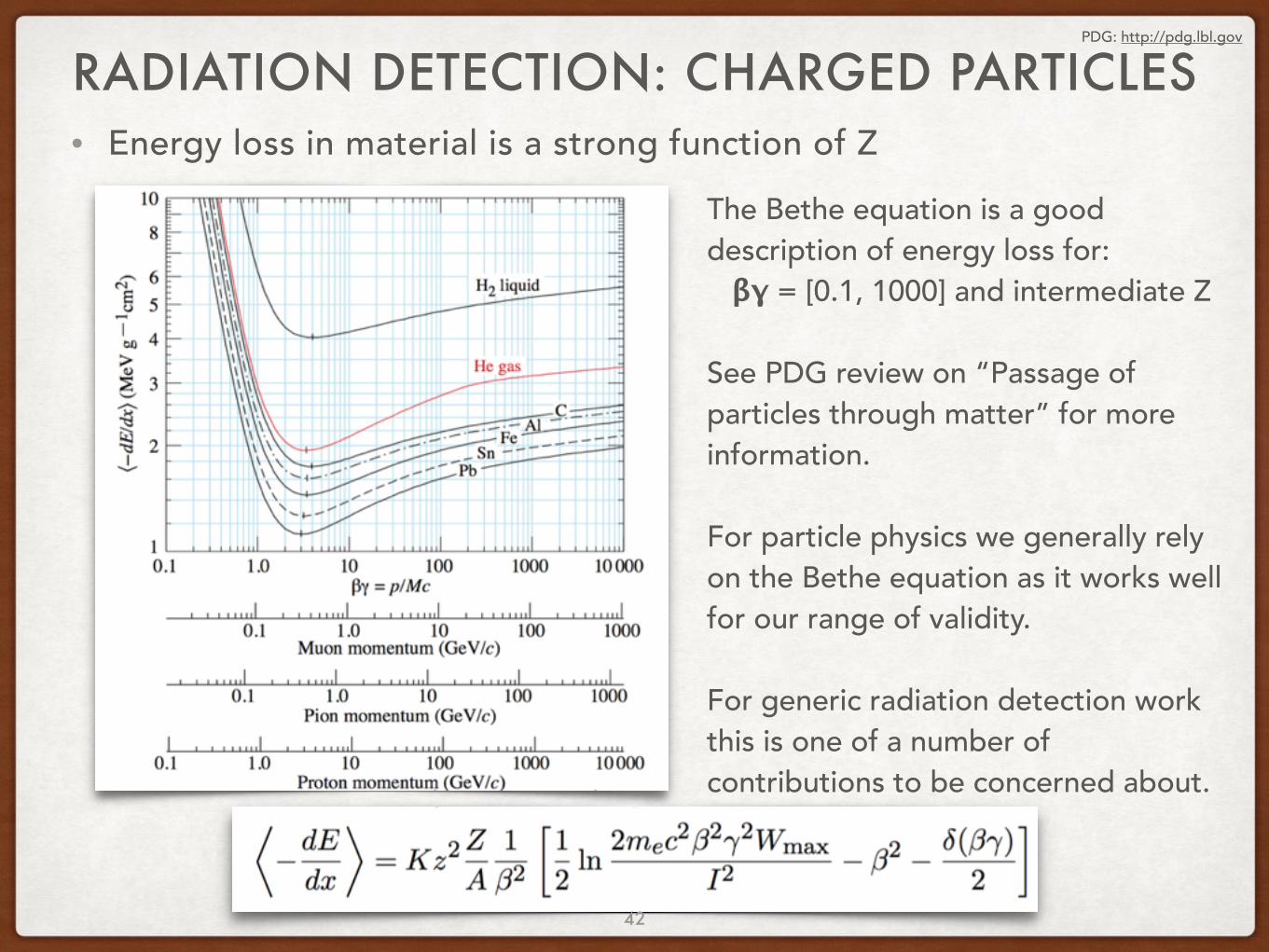
RADIATION DETECTION: CHARGED PARTICLES• Energy loss in material is a strong function of Z
The Bethe equation is a good description of energy loss for: βγ = [0.1, 1000] and intermediate Z
See PDG review on “Passage of particles through matter” for more information.
For particle physics we generally rely on the Bethe equation as it works well for our range of validity.
For generic radiation detection work this is one of a number of contributions to be concerned about.
PDG: http://pdg.lbl.gov
42
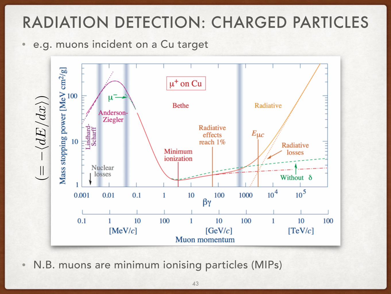
RADIATION DETECTION: CHARGED PARTICLES• e.g. muons incident on a Cu target
• N.B. muons are minimum ionising particles (MIPs)
(=�hdE/dxi)
43
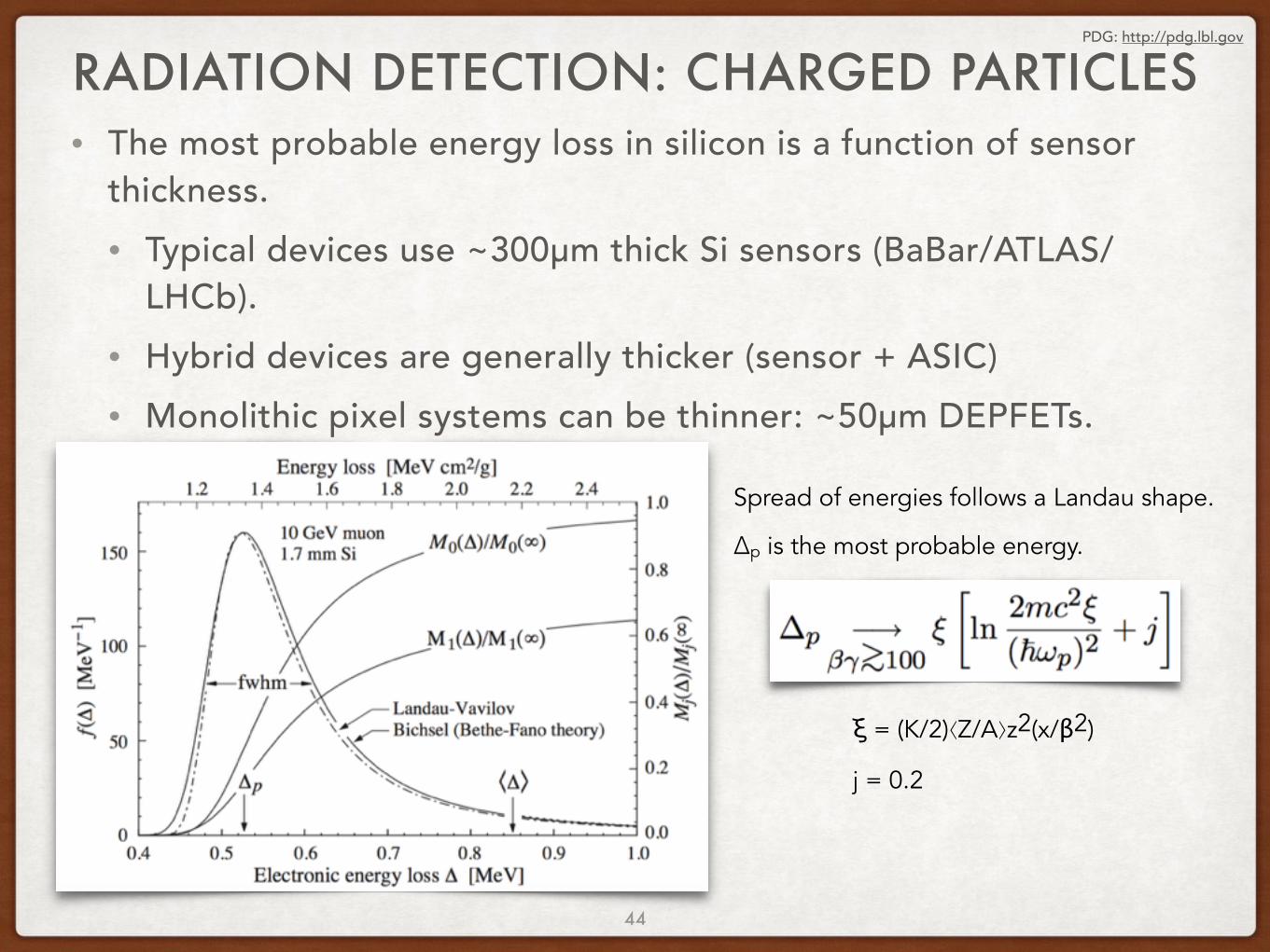
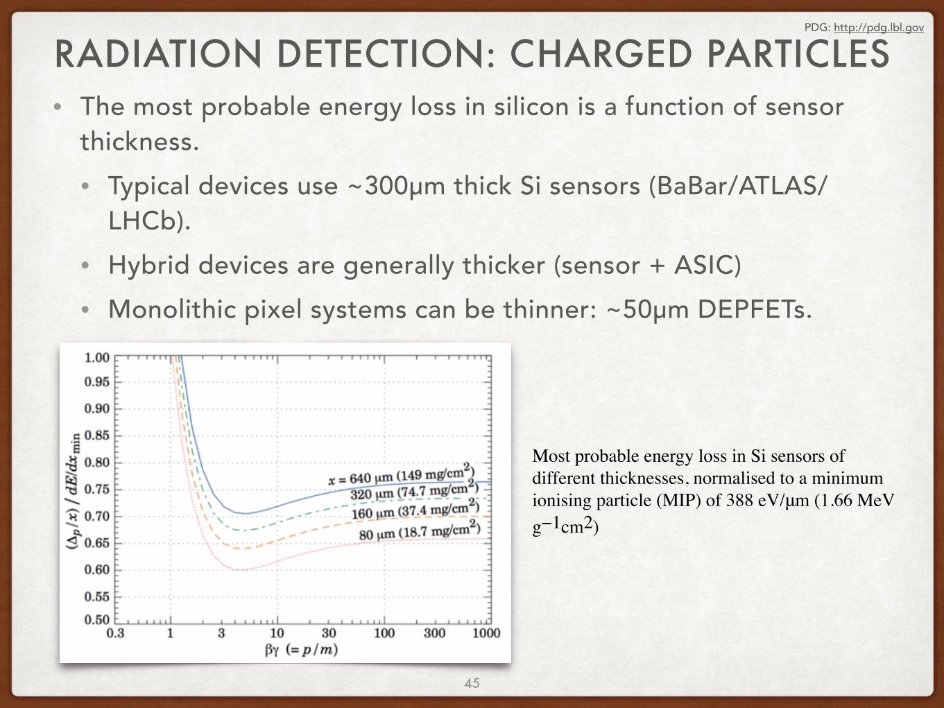
RADIATION DETECTION: CHARGED PARTICLES• The most probable energy loss in silicon is a function of sensor
thickness. • Typical devices use ~300μm thick Si sensors (BaBar/ATLAS/
LHCb). • Hybrid devices are generally thicker (sensor + ASIC) • Monolithic pixel systems can be thinner: ~50μm DEPFETs.
ξ = (K/2)⟨Z/A⟩z2(x/β2)
j = 0.2
Spread of energies follows a Landau shape.
Δp is the most probable energy.
PDG: http://pdg.lbl.gov
44
RADIATION DETECTION: CHARGED PARTICLES• The most probable energy loss in silicon is a function of sensor
thickness. • Typical devices use ~300μm thick Si sensors (BaBar/ATLAS/
LHCb). • Hybrid devices are generally thicker (sensor + ASIC) • Monolithic pixel systems can be thinner: ~50μm DEPFETs.
Most probable energy loss in Si sensors of different thicknesses, normalised to a minimum ionising particle (MIP) of 388 eV/μm (1.66 MeV g−1cm2)
PDG: http://pdg.lbl.gov
45
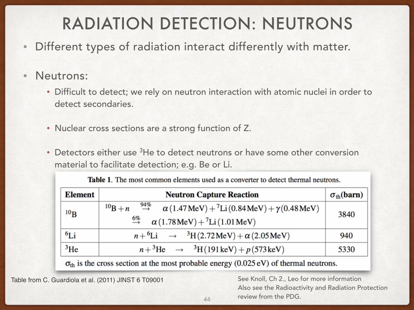
RADIATION DETECTION: NEUTRONS• Different types of radiation interact differently with matter.
• Neutrons:• Difficult to detect; we rely on neutron interaction with atomic nuclei in order to
detect secondaries.
• Nuclear cross sections are a strong function of Z.
• Detectors either use 3He to detect neutrons or have some other conversion material to facilitate detection; e.g. Be or Li.
46
See Knoll, Ch 2., Leo for more information Also see the Radioactivity and Radiation Protection review from the PDG.
Table from C. Guardiola et al. (2011) JINST 6 T09001
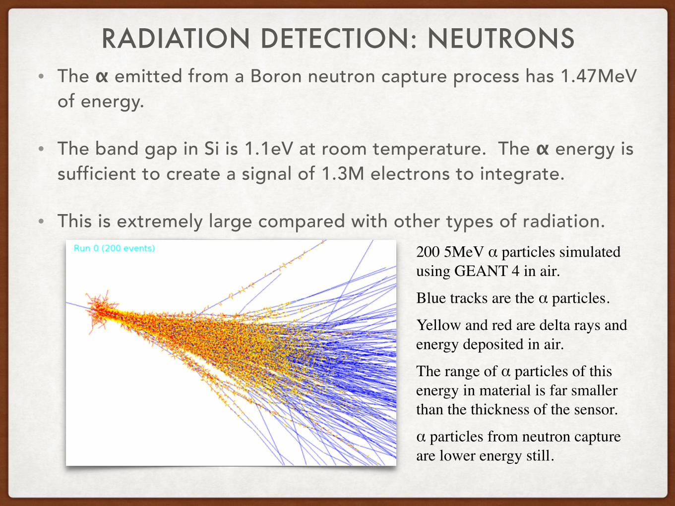
RADIATION DETECTION: NEUTRONS• The α emitted from a Boron neutron capture process has 1.47MeV
of energy.
• The band gap in Si is 1.1eV at room temperature. The α energy is sufficient to create a signal of 1.3M electrons to integrate.
• This is extremely large compared with other types of radiation.200 5MeV α particles simulated using GEANT 4 in air.
Blue tracks are the α particles.
Yellow and red are delta rays and energy deposited in air.
The range of α particles of this energy in material is far smaller than the thickness of the sensor.
α particles from neutron capture are lower energy still.

REFERENCES• The following text books provide useful reference points: Grupen,Par0cleDetectors(2011).Knoll,Radia0onDetec0onandMeasurement(2010).Krane,IntroductoryNuclearPhysics(1987).Leo,TechniquesforNuclearandPar0clePhysicsExperiments:AHow-toApproach(1984).
HelmuthSpilerhasaverygoodsetofresources(andagoodbookonthesubject):hXp://www-physics.lbl.gov/~spieler/
• In addition to these, the Particle Data Group maintain a set of review articles at the start of their “Review of Particle Physics”. These include experimental methods, statistics and other useful pieces of information.
http://pdg.lbl.gov (Then click on this link to see a list of reviews)