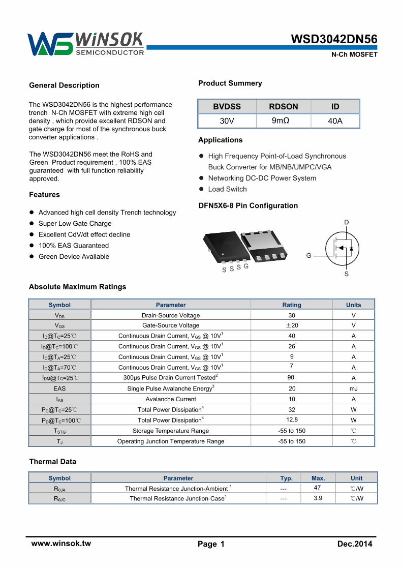
WSD3042DN56 N DFN5X6-8 30V 40A - OK
5
Symbol Parameter Rating Units V DS Drain-Source Voltage 30 V V GS Gate-Source Voltage ±20 V I D @T C =25℃ Continuous Drain Current, V GS @ 10V 1 40 A I D @T C =100℃ Continuous Drain Current, V GS @ 10V 1 26 A I D @T A =25℃ Continuous Drain Current, V GS @ 10V 1 9 A I D @T A =70℃ Continuous Drain Current, V GS @ 10V 1 7 A I DM@TC=25℃ 300μs Pulse Drain Current Tested 2 90 A EAS Single Pulse Avalanche Energy 3 20 mJ I AS Avalanche Current 10 A P D @T C =25℃ Total Power Dissipation 4 32 W P D @T C =100℃ Total Power Dissipation 4 12.8 W T STG Storage Temperature Range -55 to 150 ℃ T J Operating Junction Temperature Range -55 to 150 ℃ Symbol Parameter Typ. Max. Unit R θJA Thermal Resistance Junction-Ambient 1 --- 47 ℃/W R θJC Thermal Resistance Junction-Case 1 --- 3.9 ℃/W BVDSS RDSON ID 30V 9mΩ 40A Absolute Maximum Ratings Thermal Data General Description Features Applications 』 High Frequency Point-of-Load Synchronous Buck Converter for MB/NB/UMPC/VGA 』 Networking DC-DC Power System 』 Load Switch 』 Advanced high cell density Trench technology 』 Super Low Gate Charge 』 Excellent CdV/dt effect decline 』 100% EAS Guaranteed 』 Green Device Available DFN5X6-8 Pin Configuration Product Summery WSD3042DN56 N-Ch MOSFET Page 1 www.winsok.tw Dec.2014 The WSD3042DN56 meet the RoHS and Green Product requirement , 100% EAS guaranteed with full function reliability approved. The WSD3042DN56 is the highest performance trench N-Ch MOSFET with extreme high cell density , which provide excellent RDSON and gate charge for most of the synchronous buck converter applications .
Transcript of WSD3042DN56 N DFN5X6-8 30V 40A - OK
Symbol Parameter Rating Units VDS Drain-Source Voltage 30 V VGS Gate-Source Voltage ±20 V
ID@TC=25 Continuous Drain Current, VGS @ 10V1 40 A
ID@TC=100 Continuous Drain Current, VGS @ 10V1 26 A
ID@TA=25 Continuous Drain Current, VGS @ 10V1 9 A
ID@TA=70 Continuous Drain Current, VGS @ 10V1 7 A IDM@TC=25 300μs Pulse Drain Current Tested2 90 A
EAS Single Pulse Avalanche Energy3 20 mJ
IAS Avalanche Current 10 A
PD@TC=25 Total Power Dissipation4 32 W
PD@TC=100 Total Power Dissipation4 12.8 W
TSTG Storage Temperature Range -55 to 150
TJ Operating Junction Temperature Range -55 to 150
Symbol Parameter Typ. Max. Unit RθJA Thermal Resistance Junction-Ambient 1 --- 47 /WRθJC Thermal Resistance Junction-Case1 --- 3.9 /W
BVDSS RDSON ID
30V 9mΩ 40A
Absolute Maximum Ratings
Thermal Data
General Description
Features
Applications
High Frequency Point-of-Load Synchronous Buck Converter for MB/NB/UMPC/VGA
Networking DC-DC Power System Load Switch
Advanced high cell density Trench technology Super Low Gate Charge Excellent CdV/dt effect decline 100% EAS Guaranteed Green Device Available
DFN5X6-8 Pin Configuration
Product Summery
WSD3042DN56 N-Ch MOSFET
Page 1www.winsok.tw Dec.2014
The WSD3042DN56 meet the RoHS and Green Product requirement , 100% EAS guaranteed with full function reliability approved.
The WSD3042DN56 is the highest performance trench N-Ch MOSFET with extreme high cell density , which provide excellent RDSON and gate charge for most of the synchronous buck converter applications .
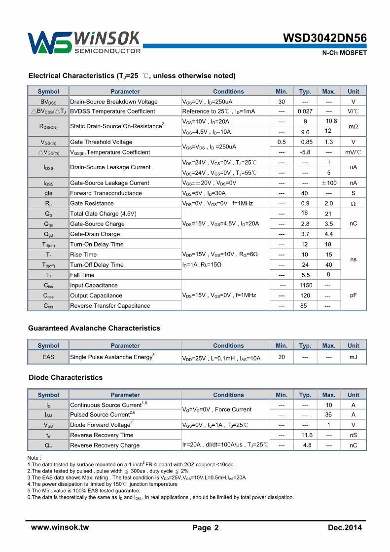
Symbol Parameter Conditions Min. Typ. Max. Unit BVDSS Drain-Source Breakdown Voltage VGS=0V , ID=250uA 30 --- --- V
BVDSS/TJ BVDSS Temperature Coefficient Reference to 25 , ID=1mA --- 0.027 --- V/
RDS(ON) Static Drain-Source On-Resistance2 VGS=10V , ID=20A --- 9 10.8
mΩVGS=4.5V , ID=10A --- 9.6 12
VGS(th) Gate Threshold Voltage VGS=VDS , ID =250uA
0.5 0.85 1.3 V
VGS(th) VGS(th) Temperature Coefficient --- -5.8 --- mV/
IDSS Drain-Source Leakage Current VDS=24V , VGS=0V , TJ=25 --- --- 1
uA VDS=24V , VGS=0V , TJ=55 --- --- 5
IGSS Gate-Source Leakage Current VGS=±20V , VDS=0V --- --- ±100 nA
gfs Forward Transconductance VDS=5V , ID=30A --- 40 --- S
Rg Gate Resistance VDS=0V , VGS=0V , f=1MHz --- 0.9 2.0 Ω
Qg Total Gate Charge (4.5V)
VDS=15V , VGS=4.5V , ID=20A
--- 16 21nC Qgs Gate-Source Charge --- 2.8 3.5
Qgd Gate-Drain Charge --- 3.7 4.4
Td(on) Turn-On Delay Time VDD=15V , VGS=10V , RG=6Ω
ID=1A ,RL=15Ω
--- 12 18
ns Tr Rise Time --- 10 15
Td(off) Turn-Off Delay Time --- 24 40
Tf Fall Time --- 5.5 8
Ciss Input Capacitance
VDS=15V , VGS=0V , f=1MHz
--- 1150
pF Coss Output Capacitance --- 120
Crss Reverse Transfer Capacitance --- 85
Symbol Parameter Conditions Min. Typ. Max. Unit
EAS Single Pulse Avalanche Energy5 VDD=25V , L=0.1mH , IAS=10A 20 --- --- mJ
Symbol Parameter Conditions Min. Typ. Max. Unit IS Continuous Source Current1,6
VG=VD=0V , Force Current --- --- 10 A
ISM Pulsed Source Current2,6 --- --- 36 A
VSD Diode Forward Voltage2 VGS=0V , IS=1A , TJ=25 --- --- 1 V
trr Reverse Recovery Time IF=20A , dI/dt=100A/µs , TJ=25
--- 11.6 --- nS
Qrr Reverse Recovery Charge --- 4.8 --- nC
Note : 1.The data tested by surface mounted on a 1 inch2 FR-4 board with 2OZ copper,t <10sec.2.The data tested by pulsed , pulse width ≦ 300us , duty cycle ≦ 2%3.The EAS data shows Max. rating . The test condition is VDD=25V,VGS=10V,L=0.5mH,IAS=20A4.The power dissipation is limited by 150 junction temperature5.The Min. value is 100% EAS tested guarantee.6.The data is theoretically the same as ID and IDM , in real applications , should be limited by total power dissipation.
Diode Characteristics
Guaranteed Avalanche Characteristics
Electrical Characteristics (TJ=25 , unless otherwise noted)
WSD3042DN56 N-Ch MOSFET
Page 2www.winsok.tw Dec.2014
---
---
---
0
25
50
75
100
0 0.5 1 1.5 2 2.5 3
ID D
rain
Cur
rent
(A)
VGS=10V
VGS=7VVGS=5V
VGS=4.5V
VGS=3V
0
2
4
6
8
10
12
0 0.3 0.6 0.9
IS - S
ourc
e C
urre
nt(A
)
TJ=150 TJ=25
0
2
4
6
8
10
0 6 12 18 24 30
VG
S , G
ate
to S
ourc
e V
olta
ge (V
)
ID=15A
VDS=24V
VDS=15V
0.2
0.6
1
1.4
1.8
-50 0 50 100 150
Nor
mal
ized
VG
S(th
)
0.2
0.6
1.0
1.4
1.8
-50 0 50 100 150
Nor
mal
ized
On
Res
ista
nce
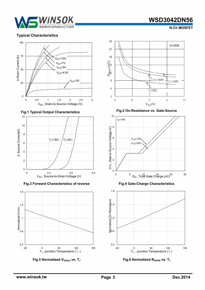
Typical Characteristics
VDS , Drain-to-Source Voltage (V)
Fig.1 T ypical Output Characteristics Fig.2 On-Resistance vs. Gate-Source
VSD , Source-to-Drain Voltage (V)
Fig.3 Forward Characteristics of reverse
QG , Total Gate Charge (nC)
Fig.4 Gate-Charge Characteristics
TJ ,Junction Temperature ( )
Fig.5 Normalized VGS(th) vs. TJ
TJ , Junction Temperature ()
Fig.6 Normalized RDSON vs. TJ
WSD3042DN56 N-Ch MOSFET
Page 3www.winsok.tw Dec.2014
ID=20A
10
100
800
10000
1 5 9 13 17 21 25VDS , Drain to Source Voltage (V)
Cap
acita
nce
(pF)
F=1.0MHz
Ciss
Coss
Crss
0.01
0.10
1.00
10.00
100.00
1000.00
0.1 1 10 100 1000
ID (A
)
10us100us
10ms100msDC
TC=25
Single Pulse
0.001
0.01
0.1
1
0.00001 0.0001 0.001 0.01 0.1 1
t , Pulse Width (s)
Nor
mal
ized
The
rmal
Res
pons
e (R
θJC)
0.01
0.05
0.1
0.2
DUTY=0.5
SINGLEPDM
D = TON/TTJpeak = TC+PDMXRθJC
TON
T
0.02
VDS (V)
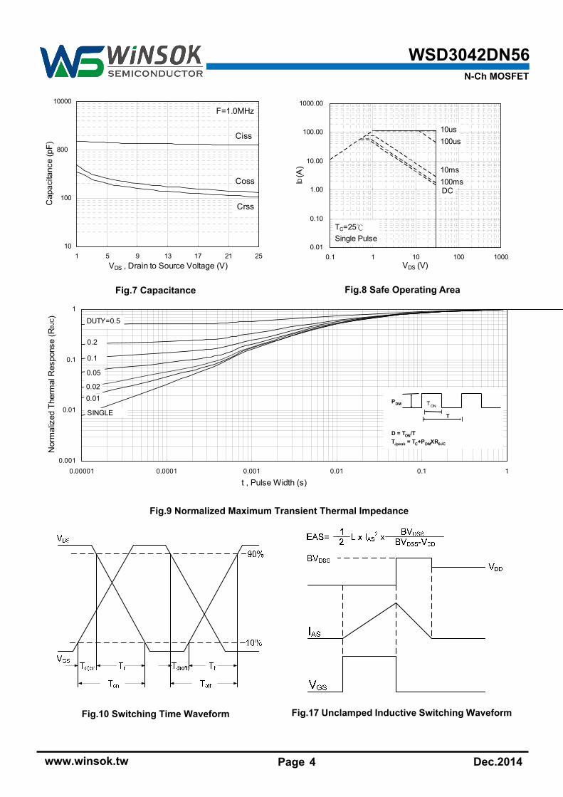
Fig.8 Safe Operating Area
Fig.9 Normalized Maximum Transient Thermal Impedance
Fig.7 Capacitance
Fig.10 Switching Time Waveform Fig.17 Unclamped Inductive Switching Waveform
WSD3042DN56 N-Ch MOSFET
Page 4www.winsok.tw Dec.2014

Attention
1, Any and all Winsok power products described or contained herein do not have specifications that can handle applications that require extremely high levels of reliability, such as life support systems, aircraft's control systems, or other applications whose failure can be reasonably expected to result in serious physical and/or material damage. Consult with your Winsok power representative nearest you before using any Winsok power products described or contained herein in such applications.
2,Winsok power assumes no responsibility for equipment failures that result from using products at values that exceed, even momentarily, rated values (such as maximum ratings, operating condition ranges, or other parameters) listed in products specifications of any and all Winsok power products described or contained herein.
3, Specifications of any and all Winsok power products described or contained herein stipulate the performance, characteristics, and functions of the described products in the independent state, and are not guarantees of the performance, characteristics, and functions of the described products as mounted in the customer’s products or equipment. Toverify symptoms and states that cannot be evaluated in an independent device, the customer should always evaluate and test devices mounted in the customer’s products or equipment.
4, Winsok power Semiconductor CO., LTD. strives to supply high quality high reliability products. However, any and all semiconductor products fail with some probability. It is possible that these probabilistic failures could give rise to accidents or events that could endanger human lives that could give rise to smoke or fire, or that could cause damage to other property. When designing equipment, adopt safety measures so that these kinds of accidents or events cannot occur. Such measures include but are not limited to protective circuits and error prevention circuits for safe design, redundant design, and structural design.
5,In the event that any or all Winsok power products(including technical data, services) described or contained herein are controlled under any of applicable local export control laws and regulations, such products must not be exported without obtaining the export license from the authorities concerned in accordance with the above law.
6, No part of this publication may be reproduced or transmitted in any form or by any means, electronic or mechanical, including photocopying and recording, or any information storage or retrieval system, or otherwise, without the prior written permission of Winsok power Semiconductor CO., LTD.
7, Information (including circuit diagrams and circuit parameters) herein is for example only; it is not guaranteed for volume production. Winsok power believes information herein is accurate and reliable, but no guarantees are made or implied regarding its use or any infringements of intellectual property rights or other rights of third parties.
8, Any and all information described or contained herein are subject to change without notice due to product/technology improvement,etc. When designing equipment, refer to the "Delivery Specification" for the Winsok power product that you Intend to use.
9, this catalog provides information as of Sep.2014. Specifications and information herein are subject to change without notice.