WIDEBAND FIXED-GAIN AMPLIFIER - Texas Instruments · •Test, Measurement, and ... JC °C/W) θ...
29
1FEATURES APPLICATIONS DESCRIPTION _ + THS4302 R f 100 Ω 49.9 Ω V I + 22 μF 47 pF 0.1 μF V S+ 50 Ω Source R g APPLICATION CIRCUIT V O + 22 μF 47 pF 0.1 μF V S- 0 2 4 6 8 10 12 14 16 10 M 100 M 1 G 10 G f - Frequency - Hz Small Signal Gain - dB SMALL SIGNAL FREQUENCY RESPONSE V O = 200 mV R L = 100 Ω V S = 5 V 30.1 Ω 30.1 Ω FB FB FB = Ferrite Bead THS4302 SLOS403H–OCTOBER 2002–REVISED AUGUST 2006 www.ti.com WIDEBAND FIXED-GAIN AMPLIFIER • Wideband Signal Processing 2• Fixed-Gain Amplifier, 5 V/V (14 dB) • Wireless Transceivers • Wide Bandwidth: 2.4 GHz • IF Amplifier • High Slew Rate: 5500 V/μs • ADC Preamplifier • Low Total Input Referred Noise: 2.8 nV/√Hz • DAC Output Buffers • Low Distortion • Test, Measurement, and Instrumentation – HD 3 : -86 dBc at 30 MHz • Medical and Industrial Imaging – HD 3 : -81 dBc at 70 MHz – IMD 3 : -88 dBc at 100 MHz – OIP 3 : 39 dBm at 100 MHz The THS4302 device is a wideband, fixed-gain – IMD 3 : -73 dBc at 300 MHz amplifier that offers high bandwidth, high slew rate, low noise, and low distortion. This combination of – OIP 3 : 32 dBm at 300 MHz specifications enables analog designers to transcend • High Output Drive: ±180 mA current performance limitations and process analog • Power Supply Voltage: 3 V or 5 V signals at much higher speeds than previously possible with closed-loop, complementary amplifier designs. This device is offered in a 16-pin leadless package and incorporates a power-down mode for quiescent power savings. 1 Please be aware that an important notice concerning availability, standard warranty, and use in critical applications of Texas Instruments semiconductor products and disclaimers thereto appears at the end of this data sheet. 2PowerPAD is a trademark of Texas Instruments. PRODUCTION DATA information is current as of publication date. Copyright © 2002–2006, Texas Instruments Incorporated Products conform to specifications per the terms of the Texas Instruments standard warranty. Production processing does not necessarily include testing of all parameters.
Transcript of WIDEBAND FIXED-GAIN AMPLIFIER - Texas Instruments · •Test, Measurement, and ... JC °C/W) θ...
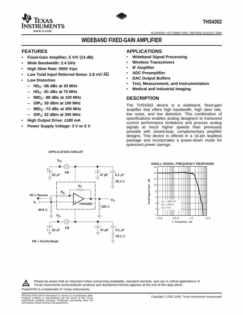
1FEATURES APPLICATIONS
DESCRIPTION
_
+THS4302
Rf
100 Ω49.9 Ω
VI
+
22 µF 47 pF 0.1 µF
VS+
50 Ω SourceRg
APPLICATION CIRCUIT
VO
+ 22 µF 47 pF 0.1 µF
VS- 0
2
4
6
8
10
12
14
16
10 M 100 M 1 G 10 G
f - Frequency - Hz
Sm
all S
ign
al G
ain
- d
B
SMALL SIGNAL FREQUENCY RESPONSE
VO = 200 mVRL = 100 ΩVS = 5 V
30.1 Ω
30.1 Ω
FB
FB
FB = Ferrite Bead
THS4302
SLOS403H–OCTOBER 2002–REVISED AUGUST 2006www.ti.com
WIDEBAND FIXED-GAIN AMPLIFIER
• Wideband Signal Processing2• Fixed-Gain Amplifier, 5 V/V (14 dB)• Wireless Transceivers• Wide Bandwidth: 2.4 GHz• IF Amplifier• High Slew Rate: 5500 V/μs• ADC Preamplifier• Low Total Input Referred Noise: 2.8 nV/√Hz• DAC Output Buffers• Low Distortion• Test, Measurement, and Instrumentation– HD3: -86 dBc at 30 MHz• Medical and Industrial Imaging
– HD3: -81 dBc at 70 MHz– IMD3: -88 dBc at 100 MHz– OIP3: 39 dBm at 100 MHz The THS4302 device is a wideband, fixed-gain– IMD3: -73 dBc at 300 MHz amplifier that offers high bandwidth, high slew rate,
low noise, and low distortion. This combination of– OIP3: 32 dBm at 300 MHzspecifications enables analog designers to transcend• High Output Drive: ±180 mA current performance limitations and process analog
• Power Supply Voltage: 3 V or 5 V signals at much higher speeds than previouslypossible with closed-loop, complementary amplifierdesigns. This device is offered in a 16-pin leadlesspackage and incorporates a power-down mode forquiescent power savings.
1
Please be aware that an important notice concerning availability, standard warranty, and use in critical applications ofTexas Instruments semiconductor products and disclaimers thereto appears at the end of this data sheet.
2PowerPAD is a trademark of Texas Instruments.
PRODUCTION DATA information is current as of publication date. Copyright © 2002–2006, Texas Instruments IncorporatedProducts conform to specifications per the terms of the TexasInstruments standard warranty. Production processing does notnecessarily include testing of all parameters.
www.ti.com
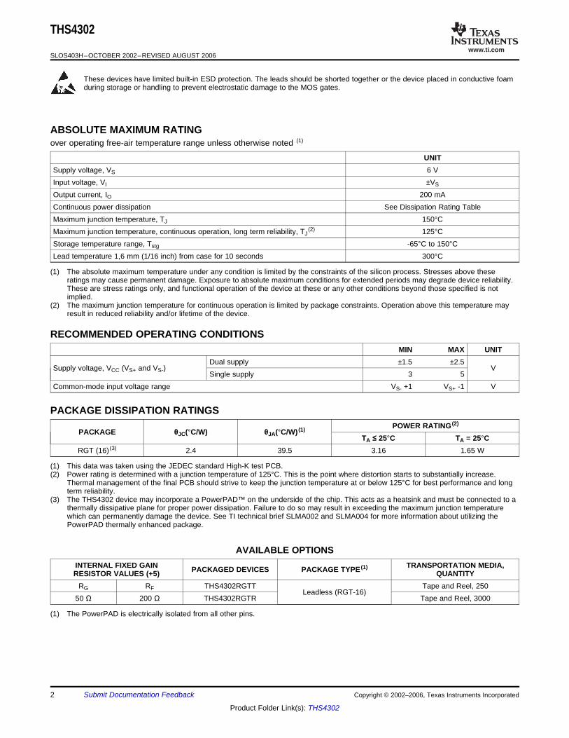
ABSOLUTE MAXIMUM RATING
RECOMMENDED OPERATING CONDITIONS
PACKAGE DISSIPATION RATINGS
THS4302
SLOS403H–OCTOBER 2002–REVISED AUGUST 2006
These devices have limited built-in ESD protection. The leads should be shorted together or the device placed in conductive foamduring storage or handling to prevent electrostatic damage to the MOS gates.
over operating free-air temperature range unless otherwise noted (1)
UNITSupply voltage, VS 6 VInput voltage, VI ±VS
Output current, IO 200 mAContinuous power dissipation See Dissipation Rating TableMaximum junction temperature, TJ 150°CMaximum junction temperature, continuous operation, long term reliability, TJ
(2) 125°CStorage temperature range, Tstg -65°C to 150°CLead temperature 1,6 mm (1/16 inch) from case for 10 seconds 300°C
(1) The absolute maximum temperature under any condition is limited by the constraints of the silicon process. Stresses above theseratings may cause permanent damage. Exposure to absolute maximum conditions for extended periods may degrade device reliability.These are stress ratings only, and functional operation of the device at these or any other conditions beyond those specified is notimplied.
(2) The maximum junction temperature for continuous operation is limited by package constraints. Operation above this temperature mayresult in reduced reliability and/or lifetime of the device.
MIN MAX UNITDual supply ±1.5 ±2.5
Supply voltage, VCC (VS+ and VS-) VSingle supply 3 5
Common-mode input voltage range VS- +1 VS+ -1 V
POWER RATING (2)PACKAGE θJC(°C/W) θJA(°C/W) (1)
TA ≤ 25°C TA = 25°CRGT (16) (3) 2.4 39.5 3.16 1.65 W
(1) This data was taken using the JEDEC standard High-K test PCB.(2) Power rating is determined with a junction temperature of 125°C. This is the point where distortion starts to substantially increase.
Thermal management of the final PCB should strive to keep the junction temperature at or below 125°C for best performance and longterm reliability.
(3) The THS4302 device may incorporate a PowerPAD™ on the underside of the chip. This acts as a heatsink and must be connected to athermally dissipative plane for proper power dissipation. Failure to do so may result in exceeding the maximum junction temperaturewhich can permanently damage the device. See TI technical brief SLMA002 and SLMA004 for more information about utilizing thePowerPAD thermally enhanced package.
AVAILABLE OPTIONSINTERNAL FIXED GAIN TRANSPORTATION MEDIA,PACKAGED DEVICES PACKAGE TYPE (1)RESISTOR VALUES (+5) QUANTITY
RG RF THS4302RGTT Tape and Reel, 250Leadless (RGT-16)
50 Ω 200 Ω THS4302RGTR Tape and Reel, 3000
(1) The PowerPAD is electrically isolated from all other pins.
2 Submit Documentation Feedback Copyright © 2002–2006, Texas Instruments Incorporated
Product Folder Link(s): THS4302
www.ti.com
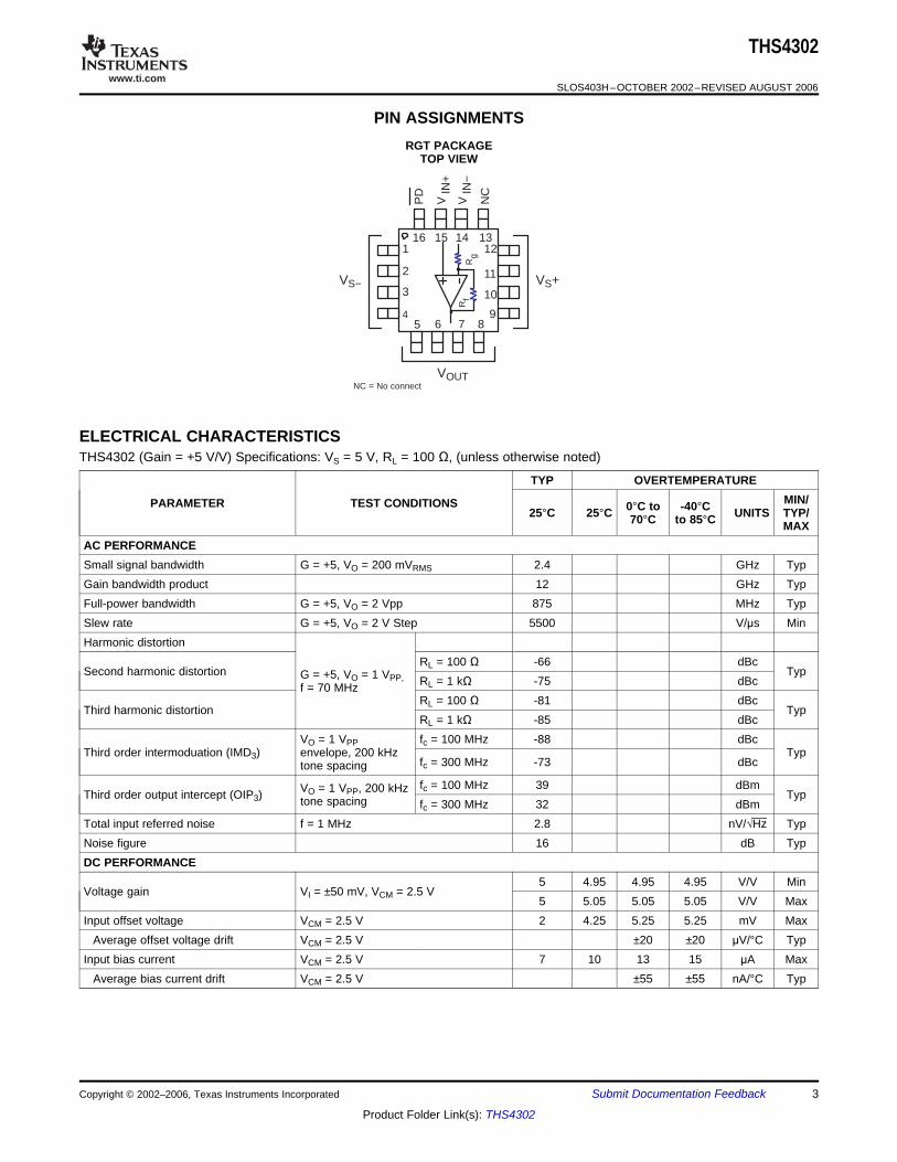
PIN ASSIGNMENTS
1
2
3
45 6 7 8
12
11
10
9
16 15 14 13
NC = No connect
VS− VS+
VOUT
VIN
+
NC
PD
VIN
−R
gR
f
ELECTRICAL CHARACTERISTICS
THS4302
SLOS403H–OCTOBER 2002–REVISED AUGUST 2006
RGT PACKAGETOP VIEW
THS4302 (Gain = +5 V/V) Specifications: VS = 5 V, RL = 100 Ω, (unless otherwise noted)
TYP OVERTEMPERATUREMIN/PARAMETER TEST CONDITIONS 0°C to -40°C25°C 25°C UNITS TYP/70°C to 85°C MAX
AC PERFORMANCESmall signal bandwidth G = +5, VO = 200 mVRMS 2.4 GHz TypGain bandwidth product 12 GHz TypFull-power bandwidth G = +5, VO = 2 Vpp 875 MHz TypSlew rate G = +5, VO = 2 V Step 5500 V/μs MinHarmonic distortion
RL = 100 Ω -66 dBcSecond harmonic distortion TypG = +5, VO = 1 VPP, RL = 1 kΩ -75 dBcf = 70 MHz
RL = 100 Ω -81 dBcThird harmonic distortion Typ
RL = 1 kΩ -85 dBcVO = 1 VPP fc = 100 MHz -88 dBc
Third order intermoduation (IMD3) envelope, 200 kHz Typfc = 300 MHz -73 dBctone spacingfc = 100 MHz 39 dBmVO = 1 VPP, 200 kHzThird order output intercept (OIP3) Typtone spacing fc = 300 MHz 32 dBm
Total input referred noise f = 1 MHz 2.8 nV/√Hz TypNoise figure 16 dB TypDC PERFORMANCE
5 4.95 4.95 4.95 V/V MinVoltage gain VI = ±50 mV, VCM = 2.5 V
5 5.05 5.05 5.05 V/V MaxInput offset voltage VCM = 2.5 V 2 4.25 5.25 5.25 mV Max
Average offset voltage drift VCM = 2.5 V ±20 ±20 μV/°C TypInput bias current VCM = 2.5 V 7 10 13 15 μA Max
Average bias current drift VCM = 2.5 V ±55 ±55 nA/°C Typ
Copyright © 2002–2006, Texas Instruments Incorporated Submit Documentation Feedback 3
Product Folder Link(s): THS4302
www.ti.com
THS4302
SLOS403H–OCTOBER 2002–REVISED AUGUST 2006
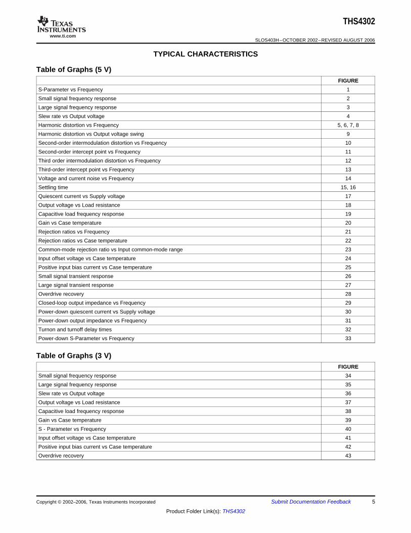
ELECTRICAL CHARACTERISTICS (continued)THS4302 (Gain = +5 V/V) Specifications: VS = 5 V, RL = 100 Ω, (unless otherwise noted)
TYP OVERTEMPERATUREMIN/PARAMETER TEST CONDITIONS 0°C to -40°C25°C 25°C UNITS TYP/70°C to 85°C MAX
INPUT CHARACTERISTICSCommon-mode input range 0.5/4.5 1/4 1.1/3.9 1.2/3.8 V MinCommon-mode rejection ratio VCM = 2 V to 3 V 60 52 50 50 dB MinInput resistance Noninverting input 1.6 MΩ TypInput capacitance Noninverting input 1 pF MaxOUTPUT CHARACTERISTICSOutput voltage swing 1/4 1.1/3.9 1.2/3.8 1.2/3.8 V MinOutput current (sourcing) RL = 5 Ω 180 170 165 160 mA MinOutput current (sinking) RL = 5 Ω 180 170 165 160 mA MinOutput impedance f = 10 MHz 0.2 Ω TypPOWER SUPPLYOperating voltage 5 5.5 5.5 5.5 V MaxMaximum quiescent current 37 42 46 48 mA MaxMinimum quiescent current 37 32 29 26 mA MinPower supply rejection ratio (PSRR +) VS+ = 5 V to 4.5 V, VS- = 0 V 60 54 52 51 dB MinPower supply rejection ratio (PSRR -) VS+ = 5 V, VS- = 0 V to 0.5 V 75 65 64 62 dB MinPOWER-DOWN CHARACTERISTICSMaximum power-down current PD = 0 V 0.8 1.0 1.1 1.2 mA MaxPower-on voltage threshold 1.1 1.5 V MinPower-down voltage threshold 1.1 0.9 V MaxTurnon time delay, td(on) 50% of final value 6 μs TypTurnoff time delay, td(off) 50% of final value 5 μs TypInput impedance 100 kΩ TypOutput impedance f = 100 kHz 250 Ω Typ
4 Submit Documentation Feedback Copyright © 2002–2006, Texas Instruments Incorporated
Product Folder Link(s): THS4302
www.ti.com
TYPICAL CHARACTERISTICS
Table of Graphs (5 V)
Table of Graphs (3 V)
THS4302
SLOS403H–OCTOBER 2002–REVISED AUGUST 2006
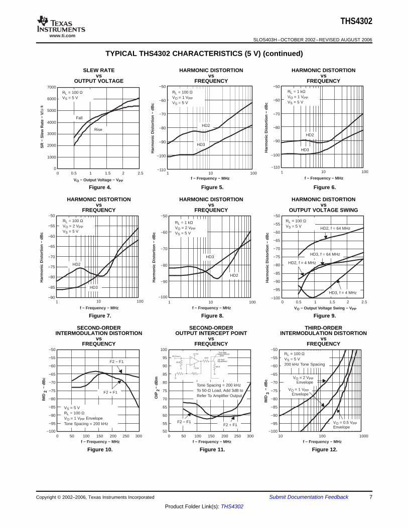
FIGURES-Parameter vs Frequency 1Small signal frequency response 2Large signal frequency response 3Slew rate vs Output voltage 4Harmonic distortion vs Frequency 5, 6, 7, 8Harmonic distortion vs Output voltage swing 9Second-order intermodulation distortion vs Frequency 10Second-order intercept point vs Frequency 11Third order intermodulation distortion vs Frequency 12Third-order intercept point vs Frequency 13Voltage and current noise vs Frequency 14Settling time 15, 16Quiescent current vs Supply voltage 17Output voltage vs Load resistance 18Capacitive load frequency response 19Gain vs Case temperature 20Rejection ratios vs Frequency 21Rejection ratios vs Case temperature 22Common-mode rejection ratio vs Input common-mode range 23Input offset voltage vs Case temperature 24Positive input bias current vs Case temperature 25Small signal transient response 26Large signal transient response 27Overdrive recovery 28Closed-loop output impedance vs Frequency 29Power-down quiescent current vs Supply voltage 30Power-down output impedance vs Frequency 31Turnon and turnoff delay times 32Power-down S-Parameter vs Frequency 33
FIGURESmall signal frequency response 34Large signal frequency response 35Slew rate vs Output voltage 36Output voltage vs Load resistance 37Capacitive load frequency response 38Gain vs Case temperature 39S - Parameter vs Frequency 40Input offset voltage vs Case temperature 41Positive input bias current vs Case temperature 42Overdrive recovery 43
Copyright © 2002–2006, Texas Instruments Incorporated Submit Documentation Feedback 5
Product Folder Link(s): THS4302
www.ti.com
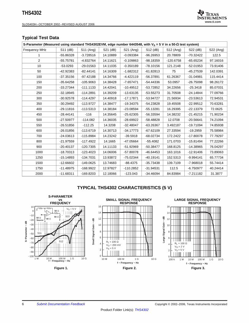
Typical Test Data
TYPICAL THS4302 CHARACTERISTICS (5 V)
−100
−90
−80
−70
−60
−50
−40
−30
−20
−10
0
10
1 M 10 M 100 M 1 G 10 Gf − Frequency − Hz
S−P
aram
eter
− d
B
S12
S11
S22
Source50 Ω
50 Ω
50 Ω50 Ω
+−
VS = 5 V
0
2
4
6
8
10
12
14
16
10 M 100 M 1 G 10 G
f − Frequency − Hz
Sm
all S
igna
l Gai
n −
dB
RL = 100 ΩVO = 200 mVVS = 5 V
0
2
4
6
8
10
12
14
16
100 k 1 M 10 M 100 M 1 G 10 G
f − Frequency − Hz
Larg
e S
igna
l Gai
n −
dB
RL = 100 ΩVO = 2 VVS = 5 V
THS4302
SLOS403H–OCTOBER 2002–REVISED AUGUST 2006
S-Parameter (Measured using standard THS4302EVM, edge number 6443548, with VS = 5 V in a 50-Ω test system)Frequency MHz S11 (dB) S11 (Ang) S21 (dB) S21 (Ang) S12 (dB) S12 (Ang) S22 (dB) S22 (Ang)
1 -55.86328 -3.728516 14.10889 -0.093384 -96.26953 20.78809 -70.32422 122.52 -55.75781 -4.832764 14.11621 -0.109863 -98.18359 -120.6758 -65.65234 97.1601610 -53.0293 -29.01563 14.11035 -0.350189 -78.10156 121.2148 -52.01953 73.9140650 -42.92383 -82.44141 14.16309 -1.682312 -61.82813 75 -45.27539 142.0391100 -37.35156 -97.42188 14.34766 -4.422119 -56.37891 61.26367 -31.04981 115.4414150 -35.64258 -105.9063 14.38428 -7.657471 -54.44336 53.0957 -26.75098 98.26172200 -33.27344 -111.1133 14.42041 -10.49512 -53.72852 34.22656 -25.3418 85.07031250 -32.18945 -114.2891 14.39209 -13.63135 -53.55273 31.70508 -24.14844 77.09766300 -30.92578 -114.4297 14.40918 -17.17871 -53.94727 21.56934 -23.53613 72.94531350 -30.29492 -113.9727 14.38477 -19.34375 -54.23828 19.45508 -22.99512 70.63281400 -29.11816 -113.5313 14.38184 -23.08594 -55.13281 16.29395 -22.13379 72.0625450 -28.44141 -116 14.35645 -25.62305 -56.33594 14.38232 -21.45215 71.90234500 -27.50977 -114.082 14.36035 -28.69922 -58.48828 12.0708 -20.56641 74.21094550 -26.51856 -112.25 14.3208 -32.48047 -63.26367 3.492187 -19.71094 74.85938600 -26.01856 -113.6719 14.30713 -34.17773 -67.62109 27.33594 -19.2959 75.58984700 -24.03613 -115.8984 14.23242 -39.5918 -68.02734 172.2422 -17.80078 77.79297800 -21.97559 -117.4922 14.1665 -47.05664 -55.4082 171.0703 -15.81494 77.22266900 -20.40137 -120.7305 14.11133 -51.92969 -50.38477 168.8125 -14.38965 76.042971000 -18.70313 -123.4023 14.06006 -57.80078 -46.64453 163.1016 -12.91406 73.890631250 -15.14893 -134.7031 13.93872 -75.02344 -40.19141 152.5313 -9.994141 65.777341500 -12.66602 -149.0625 13.74683 -88.4375 -35.73438 139.7109 -7.968018 55.744141750 -11.48975 -168.9922 12.97827 -110.2852 -31.94531 112.5 -6.750977 40.244142000 -11.68311 -169.8203 12.18066 -123.043 -34.46094 84.83984 -7.211182 31.3877
S-PARAMETERvs SMALL SIGNAL FREQUENCY LARGE SIGNAL FREQUENCY
FREQUENCY RESPONSE RESPONSE
Figure 1. Figure 2. Figure 3.
6 Submit Documentation Feedback Copyright © 2002–2006, Texas Instruments Incorporated
Product Folder Link(s): THS4302
www.ti.com
−110
−100
−90
−80
−70
−60
−50
1 10 100
HD2
HD3
Har
mon
ic D
isto
rtio
n −
dBc
f − Frequency − MHz
RL = 100 ΩVO = 1 VPPVS = 5 V
−110
−100
−90
−80
−70
−60
−50
1 10 100
HD2
HD3Har
mon
ic D
isto
rtio
n −
dBc
f − Frequency − MHz
RL = 1 kΩVO = 1 VPPVS = 5 V
0
1000
2000
3000
4000
5000
6000
7000
0 0.5 1 1.5 2 2.5
VO − Output V oltage − V PP
SR
− S
lew
Rat
e −
sµ
V/
RL = 100 ΩVS = 5 V
Fall
Rise
−90
−85
−80
−75
−70
−65
−60
−55
−50
1 10 100
HD2
HD3
Har
mon
ic D
isto
rtio
n −
dBc
f − Frequency − MHz
RL = 100 ΩVO = 2 VPPVS = 5 V
−100
−90
−80
−70
−60
−50
1 10 100
HD2
HD3
Har
mon
ic D
isto
rtio
n −
dBc
f − Frequency − MHz
RL = 1 kΩVO = 2 VPPVS = 5 V
−100
−95
−90
−85
−80
−75
−70
−65
−60
−55
−50
0 0.5 1 1.5 2 2.5
HD2, f = 64 MHz
HD3, f = 64 MHz
HD2, f = 4 MHz
HD3, f = 4 MHz
Har
mon
ic D
isto
rtio
n −
dBc
VO − Output V oltage Swing − V PP
RL = 100 ΩVS = 5 V
−100
−95
−90
−85
−80
−75
−70
−65
−60
−55
−50
0 100 300f − Frequency − MHz
VS = 5 VRL = 100 ΩVO = 1 VPP EnvelopeTone Spacing = 200 kHz
50 150 200 250
IMD
2−
dBc
F2 + F1
F2 − F1
50
55
60
65
70
75
80
85
90
95
100
0 100 300
OIP
f − Frequency − MHz
Tone Spacing = 200 kHzTo 50-Ω Load, Add 3dB toRefer To Amplifier Output
50 150 200 250
49.9
49.9
+2.5V
−2.5V49.9
50 TestEquipment
50 Source
Test datameasurement
point
2−
dBm
F2 − F1F2 + F1
−100
−95
−90
−85
−80
−75
−70
−65
−60
−55
−50
10 100 1000f − Frequency − MHz
RL = 100 ΩVS = 5 V200 kHz Tone Spacing
VO = 2 VPPEnvelope
VO = 1 VPPEnvelope
VO = 0.5 VPPEnvelope
IMD
3−
dBc
THS4302
SLOS403H–OCTOBER 2002–REVISED AUGUST 2006
TYPICAL THS4302 CHARACTERISTICS (5 V) (continued)
SLEW RATE HARMONIC DISTORTION HARMONIC DISTORTIONvs vs vs
OUTPUT VOLTAGE FREQUENCY FREQUENCY
Figure 4. Figure 5. Figure 6.
HARMONIC DISTORTION HARMONIC DISTORTION HARMONIC DISTORTIONvs vs vs
FREQUENCY FREQUENCY OUTPUT VOLTAGE SWING
Figure 7. Figure 8. Figure 9.
SECOND-ORDER SECOND-ORDER THIRD-ORDERINTERMODULATION DISTORTION OUTPUT INTERCEPT POINT INTERMODULATION DISTORTION
vs vs vsFREQUENCY FREQUENCY FREQUENCY
Figure 10. Figure 11. Figure 12.
Copyright © 2002–2006, Texas Instruments Incorporated Submit Documentation Feedback 7
Product Folder Link(s): THS4302
www.ti.com
1.75
2
2.25
2.5
2.75
3
3.25
0.2 0 0.2 0.4 0.6 0.8 1 1.2
RL = 100 Ωf= 1 MHzVS = 5 V
Rising Edge
Falling Edge
t − Time − ns
− O
utpu
t Vol
tage
− V
V O
1
10
100
100 1 k 10 k 100 k 1 M 10 M1
10
100
Vn
In
f − Frequency − Hz
− Vo
ltage
Noi
se −
nV/
Hz
Vn
− C
urre
nt N
oise
−pA
/H
zI n
25
27
29
31
33
35
37
39
41
43
0 100 200 300 400 500
f − Frequency − MHz
RL = 100 ΩVS = 5 V
VO = 1 VPPEnvelope
49.9
49.9
+2.5V
−2.5V49.9
50 TestEquipment
50 Source
Test datameasurement
point
OIP
3−
dBm
Tone Spacing = 200 kHzTo 50-Ω Load, Add 3dB toRefer To Amplifier Output
1
1.25
1.5
1.75
2
2.25
2.5
2.75
3
3.25
3.5
3.75
4
0.2 0 0.2 0.4 0.6 0.8 1 1.2 1.4 1.6
RL = 100 Ωf= 1 MHzVS = 5 V
Rising Edge
Falling Edge
t − Time − ns
− O
utpu
t Vol
tage
− V
V O
0
0.5
1
1.5
2
2.5
3
3.5
4
4.5
5
1 10 100 1000
RL − Load Resistance − Ω
− O
utpu
t Vol
tage
− V
V O
VS = 5 VTA = −40 to 85°C
0
5
10
15
20
25
30
35
40
45
50
2.5 3 3.5 4 4.5 5
VS − Supply V oltage − V
Qui
esce
nt C
urre
nt −
mA
TA = 85°C
TA = 25°C
TA = −40°C
−3
−2.5
−2
−1.5
−1
−0.5
0
0.5
10 M 100 M 1 G
1
f − Frequency − Hz
Nor
mal
ized
Gai
n −
dB
R(ISO) = 12.1 Ω,CL = 47 pF
VS = 5 V
R(ISO) = 8 Ω,CL = 100 pF
R(ISO) = 24.9 Ω, CL = 10 pF
13.92
13.94
13.96
13.98
14
14.02
−40−30−20−10 0 10 20 30 40 50 60 70 80 90
Gai
n −d
B
Case Temperature − °C
VS = 5 V
0
10
20
30
40
50
60
70
100 k 1 M 10 M 100 M 1 G
CMRR
PSRR+
VS = 5 V
Rej
ectio
n R
atio
s −
dB
f − Frequency − Hz
THS4302
SLOS403H–OCTOBER 2002–REVISED AUGUST 2006
TYPICAL THS4302 CHARACTERISTICS (5 V) (continued)
THIRD-ORDEROUTPUT INTERCEPT POINT VOLTAGE AND CURRENT NOISE
vs vsFREQUENCY FREQUENCY SETTLING TIME
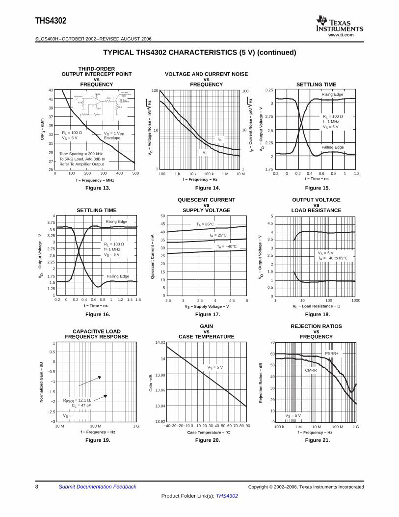
Figure 13. Figure 14. Figure 15.
QUIESCENT CURRENT OUTPUT VOLTAGEvs vs
SETTLING TIME SUPPLY VOLTAGE LOAD RESISTANCE
Figure 16. Figure 17. Figure 18.
GAIN REJECTION RATIOSCAPACITIVE LOAD vs vs
FREQUENCY RESPONSE CASE TEMPERATURE FREQUENCY
Figure 19. Figure 20. Figure 21.
8 Submit Documentation Feedback Copyright © 2002–2006, Texas Instruments Incorporated
Product Folder Link(s): THS4302
www.ti.com
−10
0
10
20
30
40
50
60
70
0 1 2 3 4 5
VICR − Input Common-Mode V oltage Range − V
CM
RR
− C
omm
on-M
ode
Rej
ectio
n R
atio
− d
BVS = 5 V
40
45
50
55
60
65
70
75
80
−40−30−20−10 0 10 20 30 40 50 60 70 80 90
Rej
ectio
n R
atio
s −
dB
Case Temperature − °C
PSRR+
VS = 5 V
PSRR−
CMMR
0
1
2
3
4
5
6
−40−30−20−10 0 10 20 30 40 50 60 70 80 90
Case Temperature − °C
− In
put O
ffset
Vol
tage
− m
VV
OS
VS = 5 V
2.35
2.4
2.45
2.5
2.55
2.6
2.65
0 2 4 6 8 10 12 14 16 18 20
RL = 100 ΩInput tr/tf = 60 psVS = 5 V
1
1.5
2
2.5
3
3.5
4
0 2 4 6 8 10 12 14 16 18 20
t − Time − ns
− O
utpu
t Vol
tage
− V
V O RL = 100 ΩInput tr/tf = 60 psVS = 5 V
0
2
4
6
8
10
12
−40−30−20−10 0 10 20 30 40 50 60 70 80 90
VS = 5 V
− P
ositi
ve In
put B
ias
Cur
rent
−I I
B+
Aµ
Case Temperature − °C
−0.5
0
0.5
1
1.5
2
2.5
3
3.5
4
4.5
5
5.5
0 0.1 0.2 0.3 0.4 0.5 0.6 0.7 0.8 0.9 12
2.25
2.5
2.75
3
t − Time − µs
Sin
gle-
End
ed O
utpu
t Vol
tage
− V
− In
put V
olta
ge −
VV
I
0.1
1
10
100
10 M 100 M 1 G 10 Gf − Frequency − Hz
Out
put I
mpe
danc
e −
Ω
VS = 5 V
0
100
200
300
400
500
600
700
800
900
1000
1100
1200
2.5 2.75 3 3.25 3.5 3.75 4 4.25 4.5 4.75 5
VS − Supply V oltage − V
Pow
er-D
own
Qui
esce
nt C
urre
nt −
TA = 85°C
TA = 25°C
Aµ
TA = −40°C
THS4302
SLOS403H–OCTOBER 2002–REVISED AUGUST 2006
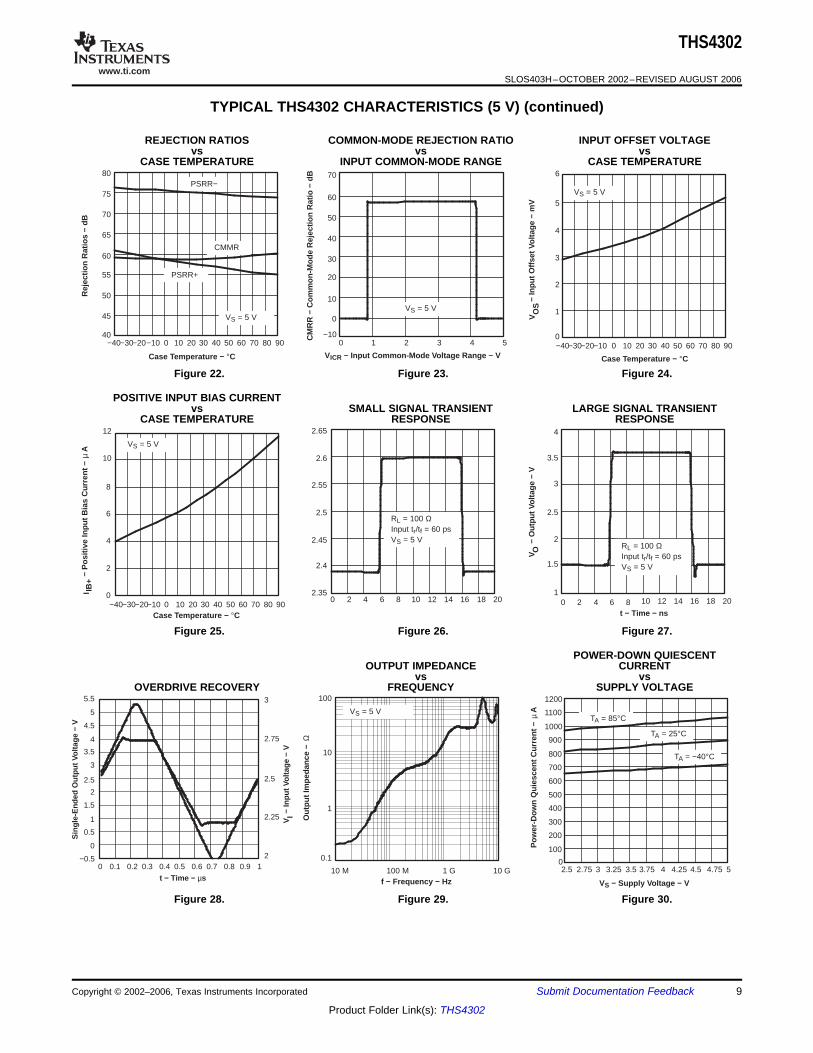
TYPICAL THS4302 CHARACTERISTICS (5 V) (continued)
REJECTION RATIOS COMMON-MODE REJECTION RATIO INPUT OFFSET VOLTAGEvs vs vs
CASE TEMPERATURE INPUT COMMON-MODE RANGE CASE TEMPERATURE
Figure 22. Figure 23. Figure 24.
POSITIVE INPUT BIAS CURRENTvs SMALL SIGNAL TRANSIENT LARGE SIGNAL TRANSIENT
CASE TEMPERATURE RESPONSE RESPONSE
Figure 25. Figure 26. Figure 27.
POWER-DOWN QUIESCENTOUTPUT IMPEDANCE CURRENT
vs vsOVERDRIVE RECOVERY FREQUENCY SUPPLY VOLTAGE
Figure 28. Figure 29. Figure 30.
Copyright © 2002–2006, Texas Instruments Incorporated Submit Documentation Feedback 9
Product Folder Link(s): THS4302
www.ti.com
10
100
1000
100 k 1 M 10 M 100 M 1 G
f − Frequency − Hz
Pow
er-D
own
Out
put I
mpe
danc
e −
Ω
VS = 5 V
−10
0
10
20
30
40
50
60
70
80
−15 0 15 30 45 60 75
−6
−5
−4
−3
−2
−1
0
1
2
3
t − Time − µs
− O
utpu
t Cur
rent
Lev
el −
mA
I ORL = 100 ΩVS = 5 V
− In
put V
olta
ge L
evel
− V
VI
−100
−90
−80
−70
−60
−50
−40
−30
−20
−10
0
10
1 M 10 M 100 M 1 G 10 G
f − Frequency − Hz
Pow
erdo
wn
S−P
aram
eter
− d
B
S12
S11
S22
Source
C
50 Ω
50 Ω
50 Ω50 Ω
RFRG
+−
VS = 5 V and 3 V
TYPICAL THS4302 CHARACTERISTICS (3 V)
0
2
4
6
8
10
12
14
16
100 k 1 M 10 M 100 M 1 G 10 G
f − Frequency − Hz
Sm
all S
igna
l Gai
n −
dB
RL = 100 ΩVO = 100 mVVS = 3 V
0
2
4
6
8
10
12
14
16
100 k 1 M 10 M 100 M 1G 10 Gf − Frequency − Hz
RL = 100 ΩVO = 0.5 VVS = 3 V
Larg
e S
igna
l Gai
n −
dB
0
500
1000
1500
2000
2500
3000
3500
4000
0 0.25 0.5 0.75 1 1.25 1.5VO − Output V oltage − V
SR
− S
lew
Rat
e −
sµ
V/
RL = 100 ΩVS = 3 V
Fall
Rise
0.75
1
1.25
1.5
1.75
2
2.25
1 10 100 1000
RL − Load Resistance − Ω
− O
utpu
t Vol
tage
− V
V O
VS = 3 VTA = −40 to 85°C
−3
−2.5
−2
−1.5
−1
−0.5
0
0.5
10 M 100 M 1 G
1
f − Frequency − Hz
Nor
mal
ized
Gai
n −
dB
R(ISO) = 12.1 Ω,CL = 47 pF
RL = 100 Ω,VS = 5 V
R(ISO) = 8 Ω,CL = 100 pF
R(ISO) = 24.9 Ω, CL = 10 pF
13.92
13.94
13.96
13.98
14
14.02
14.04
−40−30−20−10 0 10 20 30 40 50 60 70 80 90
Gai
n −
dB
Case Temperature − °C
VS = 3 V
THS4302
SLOS403H–OCTOBER 2002–REVISED AUGUST 2006
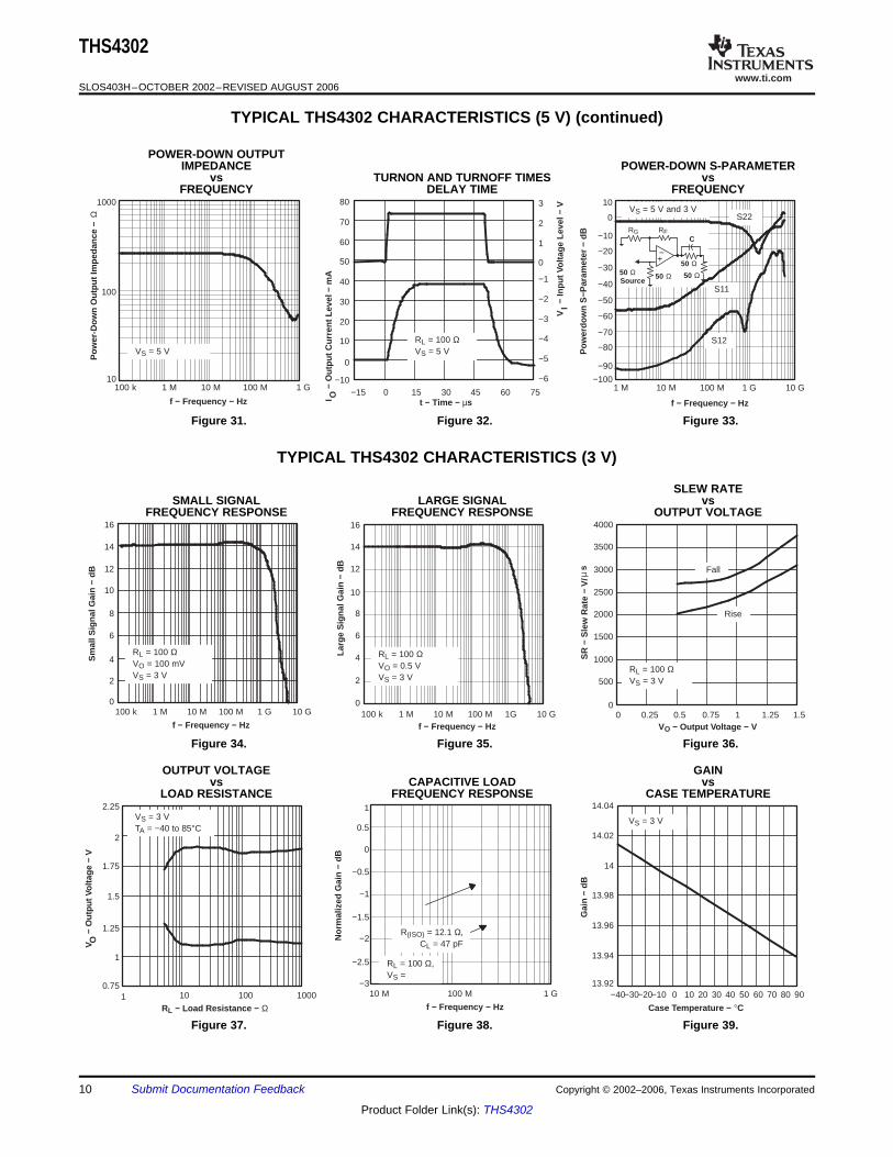
TYPICAL THS4302 CHARACTERISTICS (5 V) (continued)
POWER-DOWN OUTPUTIMPEDANCE POWER-DOWN S-PARAMETER
vs TURNON AND TURNOFF TIMES vsFREQUENCY DELAY TIME FREQUENCY
Figure 31. Figure 32. Figure 33.
SLEW RATESMALL SIGNAL LARGE SIGNAL vs
FREQUENCY RESPONSE FREQUENCY RESPONSE OUTPUT VOLTAGE
Figure 34. Figure 35. Figure 36.
OUTPUT VOLTAGE GAINvs CAPACITIVE LOAD vs
LOAD RESISTANCE FREQUENCY RESPONSE CASE TEMPERATURE
Figure 37. Figure 38. Figure 39.
10 Submit Documentation Feedback Copyright © 2002–2006, Texas Instruments Incorporated
Product Folder Link(s): THS4302
www.ti.com
−100
−90
−80
−70
−60
−50
−40
−30
−20
−10
0
10
1 M 10 M 100 M 1 G 10 G
f − Frequency − Hz
S−P
aram
eter
− d
B Source
C
50 Ω
50 Ω
50 Ω50 Ω
RFRG VS = 3 V
S22
S11
S12
+−
0
2
4
6
8
10
12
−40−30−20−10 0 10 20 30 40 50 60 70 80 90
− P
ositi
ve In
put B
ias
Cur
rent
−
Case Temperature − °C
VS = 3 V
I IB
+A
µ
0
0.5
1
1.5
2
2.5
3
3.5
4
−40−30−20−10 0 10 20 30 40 50 60 70 80 90
VS = 3 V
Case Temperature − °C
− In
put O
ffset
Vol
tage
− m
VV
OS
0
0.25
0.5
0.75
1
1.25
1.5
1.75
2
2.25
2.5
2.75
3
0 0.1 0.2 0.3 0.4 0.5 0.6 0.7 0.8 0.9 1
1.25
1.375
1.5
1.625
1.75
t − Time − µs
− In
put V
olta
ge −
VV
I
VS = 3 V
− O
utpu
t Vol
tage
− V
V O
THS4302
SLOS403H–OCTOBER 2002–REVISED AUGUST 2006
TYPICAL THS4302 CHARACTERISTICS (3 V) (continued)
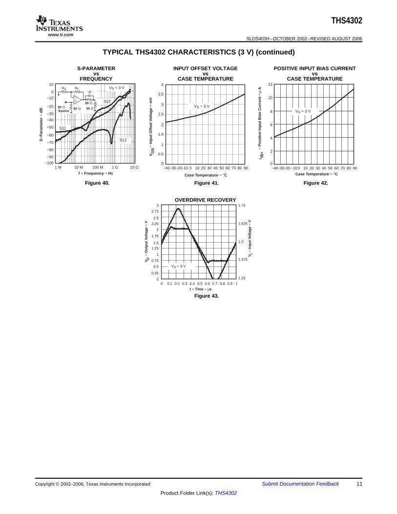
S-PARAMETER INPUT OFFSET VOLTAGE POSITIVE INPUT BIAS CURRENTvs vs vs
FREQUENCY CASE TEMPERATURE CASE TEMPERATURE
Figure 40. Figure 41. Figure 42.
OVERDRIVE RECOVERY
Figure 43.
Copyright © 2002–2006, Texas Instruments Incorporated Submit Documentation Feedback 11
Product Folder Link(s): THS4302
www.ti.com
APPLICATION INFORMATION
High-Speed Operational amplifiers
Applications Section Contents
_
+THS4302
Rf
100 Ω49.9 Ω
VI
+
22 µF 47 pF 0.1 µF
VS+
50-Ω SourceRg
VO
+ 22 µF 47 pF 0.1 µF
VS−
30.1 Ω
30.1 Ω
FB
FB
FB = Ferrite Bead
THS4302
SLOS403H–OCTOBER 2002–REVISED AUGUST 2006
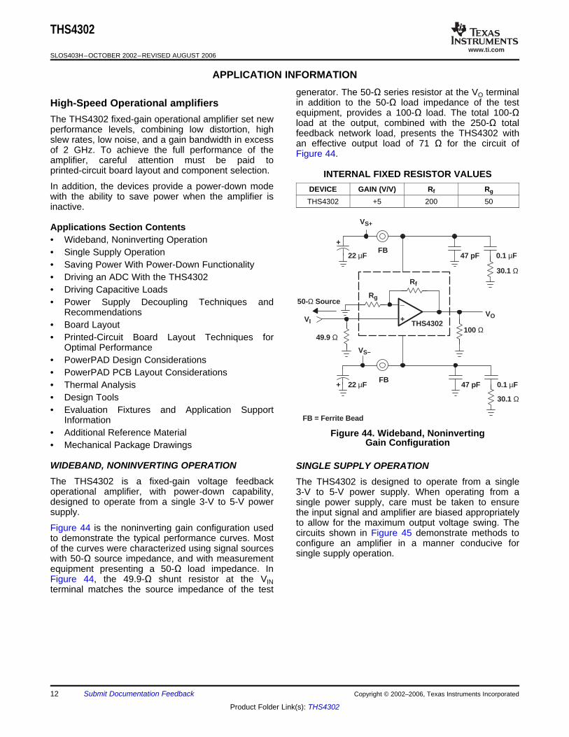
generator. The 50-Ω series resistor at the VO terminalin addition to the 50-Ω load impedance of the testequipment, provides a 100-Ω load. The total 100-Ω
The THS4302 fixed-gain operational amplifier set new load at the output, combined with the 250-Ω totalperformance levels, combining low distortion, high feedback network load, presents the THS4302 withslew rates, low noise, and a gain bandwidth in excess an effective output load of 71 Ω for the circuit ofof 2 GHz. To achieve the full performance of the Figure 44.amplifier, careful attention must be paid toprinted-circuit board layout and component selection. INTERNAL FIXED RESISTOR VALUESIn addition, the devices provide a power-down mode DEVICE GAIN (V/V) Rf Rgwith the ability to save power when the amplifier is THS4302 +5 200 50inactive.
• Wideband, Noninverting Operation• Single Supply Operation• Saving Power With Power-Down Functionality• Driving an ADC With the THS4302• Driving Capacitive Loads• Power Supply Decoupling Techniques and
Recommendations• Board Layout• Printed-Circuit Board Layout Techniques for
Optimal Performance• PowerPAD Design Considerations• PowerPAD PCB Layout Considerations• Thermal Analysis• Design Tools• Evaluation Fixtures and Application Support
Information• Additional Reference Material Figure 44. Wideband, Noninverting
Gain Configuration• Mechanical Package Drawings
WIDEBAND, NONINVERTING OPERATION SINGLE SUPPLY OPERATIONThe THS4302 is a fixed-gain voltage feedback The THS4302 is designed to operate from a singleoperational amplifier, with power-down capability, 3-V to 5-V power supply. When operating from adesigned to operate from a single 3-V to 5-V power single power supply, care must be taken to ensuresupply. the input signal and amplifier are biased appropriately
to allow for the maximum output voltage swing. TheFigure 44 is the noninverting gain configuration used circuits shown in Figure 45 demonstrate methods toto demonstrate the typical performance curves. Most configure an amplifier in a manner conducive forof the curves were characterized using signal sources single supply operation.with 50-Ω source impedance, and with measurementequipment presenting a 50-Ω load impedance. InFigure 44, the 49.9-Ω shunt resistor at the VINterminal matches the source impedance of the test
12 Submit Documentation Feedback Copyright © 2002–2006, Texas Instruments Incorporated
Product Folder Link(s): THS4302
www.ti.com
APPLICATION CIRCUITS
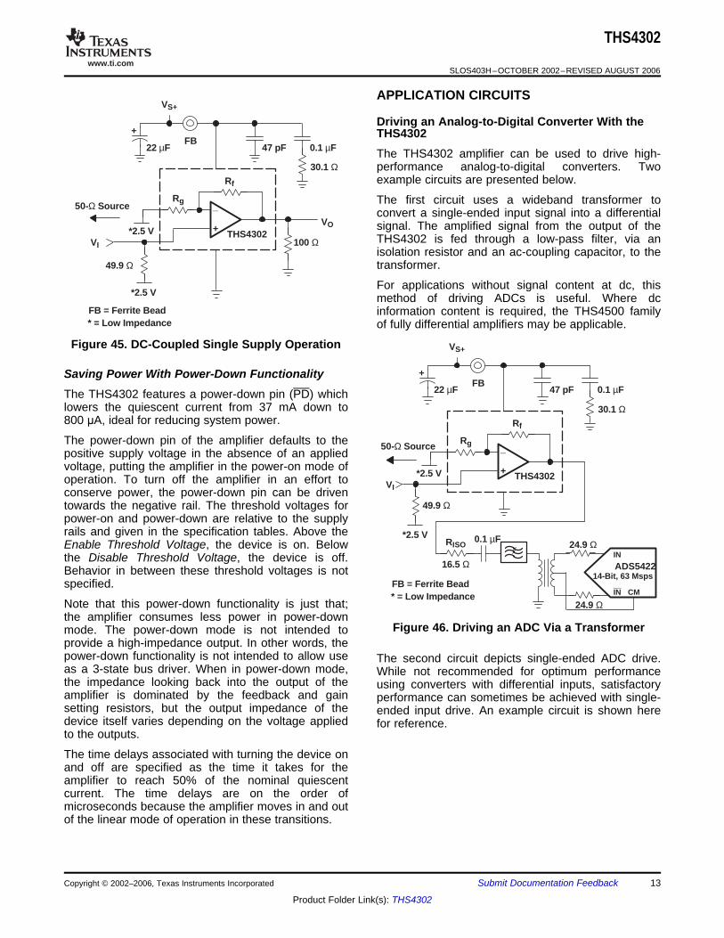
Driving an Analog-to-Digital Converter With the
_
+THS4302
Rf
100 Ω
49.9 Ω
VI
+
22 µF 47 pF 0.1 µF
VS+
50-Ω SourceRg
VO
30.1 Ω
FB
FB = Ferrite Bead
*2.5 V
*2.5 V
* = Low Impedance
ADS542214-Bit, 63 Msps
RISO0.1 µF
24.9 Ω
_
+ THS4302
Rf
49.9 Ω
VI
+
22 µF 47 pF 0.1 µF
VS+
50-Ω SourceRg
30.1 Ω
FB
FB = Ferrite Bead
*2.5 V
*2.5 V
* = Low Impedance
24.9 Ω
16.5 Ω
IN
IN
CM
THS4302
SLOS403H–OCTOBER 2002–REVISED AUGUST 2006
THS4302The THS4302 amplifier can be used to drive high-performance analog-to-digital converters. Twoexample circuits are presented below.
The first circuit uses a wideband transformer toconvert a single-ended input signal into a differentialsignal. The amplified signal from the output of theTHS4302 is fed through a low-pass filter, via anisolation resistor and an ac-coupling capacitor, to thetransformer.
For applications without signal content at dc, thismethod of driving ADCs is useful. Where dcinformation content is required, the THS4500 familyof fully differential amplifiers may be applicable.
Figure 45. DC-Coupled Single Supply Operation
Saving Power With Power-Down FunctionalityThe THS4302 features a power-down pin (PD) whichlowers the quiescent current from 37 mA down to800 μA, ideal for reducing system power.
The power-down pin of the amplifier defaults to thepositive supply voltage in the absence of an appliedvoltage, putting the amplifier in the power-on mode ofoperation. To turn off the amplifier in an effort toconserve power, the power-down pin can be driventowards the negative rail. The threshold voltages forpower-on and power-down are relative to the supplyrails and given in the specification tables. Above theEnable Threshold Voltage, the device is on. Belowthe Disable Threshold Voltage, the device is off.Behavior in between these threshold voltages is notspecified.
Note that this power-down functionality is just that;the amplifier consumes less power in power-down
Figure 46. Driving an ADC Via a Transformermode. The power-down mode is not intended toprovide a high-impedance output. In other words, thepower-down functionality is not intended to allow use The second circuit depicts single-ended ADC drive.as a 3-state bus driver. When in power-down mode, While not recommended for optimum performancethe impedance looking back into the output of the using converters with differential inputs, satisfactoryamplifier is dominated by the feedback and gain performance can sometimes be achieved with single-setting resistors, but the output impedance of the ended input drive. An example circuit is shown heredevice itself varies depending on the voltage applied for reference.to the outputs.
The time delays associated with turning the device onand off are specified as the time it takes for theamplifier to reach 50% of the nominal quiescentcurrent. The time delays are on the order ofmicroseconds because the amplifier moves in and outof the linear mode of operation in these transitions.
Copyright © 2002–2006, Texas Instruments Incorporated Submit Documentation Feedback 13
Product Folder Link(s): THS4302
www.ti.com
ADS80712-Bit,
53 Msps
RISO 0.1 µF
16.5 Ω 68 pf
0.1 µF
IN
IN
CM
1.82 kΩ
_
+THS4302
Rf
49.9 Ω
VI
+
22 µF 47 pF 0.1 µF
VS+
50-Ω SourceRg
30.1 Ω
FB
FB = Ferrite Bead
*2.5 V
*2.5 V
* = Low Impedance
-3
-2.5
-2
-1.5
-1
-0.5
0
0.5
10 M 100 M 1 G
1
f - Frequency - Hz
No
rmal
ized
Gai
n -
dB
R(ISO) = 12.1 Ω,CL = 47 pF
VS = 5 V
R(ISO) = 8 Ω,CL = 100 pF
R(ISO) = 24.9 Ω, CL = 10 pF
Power Supply Decoupling Techniques andDriving Capacitive Loads
THS4302
SLOS403H–OCTOBER 2002–REVISED AUGUST 2006
The Typical Characteristics show the recommendedisolation resistor vs capacitive load and the resultingfrequency response at the load. Parasitic capacitiveloads greater than 2 pF can begin to degrade theperformance of the THS4302. Long PC board traces,unmatched cables, and connections to multipledevices can easily cause this value to be exceeded.Always consider this effect carefully, and add therecommended series resistor as close as possible tothe THS4302 output pin (see Board LayoutGuidelines).
The criterion for setting this R(ISO) resistor is amaximum bandwidth, flat frequency response at theload.
For best performance, high-speed ADCsshould be driven differentially. See theTHS4500 family of devices for moreinformation.
Figure 47. Driving an ADC With a Single-EndedFigure 48. Driving Capacitive LoadsInput
RecommendationsOne of the most demanding, and yet very common,
Power supply decoupling is a critical aspect of anyload conditions for an op amp is capacitive loading.high-performance amplifier design process. CarefulOften, the capacitive load is the input of an A/Ddecoupling provides higher quality ac performanceconverter, including additional external capacitance,(most notably improved distortion performance). Thewhich may be recommended to improve A/D linearity.following guidelines ensure the highest level ofHigh-speed amplifiers like the THS4302 can beperformance.susceptible to decreased stability and closed-loop
response peaking when a capacitive load is placed 1. Place decoupling capacitors as close to thedirectly on the output pin. When the amplifier's power supply inputs as possible, with the goal ofopen-loop output resistance is considered, this minimizing the inductance of the path fromcapacitive load introduces an additional pole in the ground to the power supply. Inductance in seriessignal path that can decrease the phase margin. with the bypass capacitors will degradeWhen the primary considerations are frequency performance. Note that a narrow lead or traceresponse flatness, pulse response fidelity, or has about 0.8 nH of inductance for everydistortion, the simplest and most effective solution is millimeter of length. Each printed-circuit boardto isolate the capacitive load from the feedback loop (PCB) via also has between 0.3 and 0.8 nHby depending on length and diameter. For theseinserting a series isolation resistor between the reasons, it is recommended to use a poweramplifier output and the capacitive load. supply trace about the width of the package for
each power supply lead to the capacitors, and 3or more vias to connect the capacitors to theground plane.
2. Placement priority should put the smallest valuedcapacitors closest to the device.
3. Solid power planes can lead to PCB resonances
14 Submit Documentation Feedback Copyright © 2002–2006, Texas Instruments Incorporated
Product Folder Link(s): THS4302
www.ti.com
BOARD LAYOUT
Printed-Circuit Board Layout Techniques for
frequencyres n (44GHz mm)
where:frequencyres = the approximate power plane resonant frequencies in GHz = the length of the power plane dimensions in millimetersn = an integer (n > 1) related to the mode of the oscillation
THS4302
SLOS403H–OCTOBER 2002–REVISED AUGUST 2006
when they are not properly terminated to the 6. Recommended values for power supplyground plane over the area and along the decoupling include a bulk decoupling capacitorperimeter of the power plane by high frequency (22 μF), a ferrite bead with a high self-resonantcapacitors. Doing so ensures that there are no frequency, a mid-range decoupling capacitor (0.1power plane resonances in the needed frequency μF) in series with a 30.1-Ω resistor, and arange. Values used are in the range of 2 pF - 50 high-frequency decoupling capacitor (47 pF).pF, depending on the frequencies to besuppressed, with numerous vias for each. Using0402 or smaller component sizes isrecommended. An approximate expression forthe resonant frequencies associated with a length Optimal Performanceof one of the power plane dimensions is given in
Achieving optimum performance with a highthe following equation. Note that a power plane offrequency amplifier like the THS4302 requires carefularbitrary shape can have a number of resonantattention to board layout parasitics and externalfrequencies. A power plane without distributedcomponent types.capacitors and with active parts near the center
of the plane usually has n even (≥ 2) due to the Recommendations that optimize performance include:half wave resonant nature of the plane. 1. Minimize parasitic capacitance to any ac
ground for all of the signal I/O pins. However,if using a transmission line at the I/O, then placethe matching resistor as close to the part aspossible. Except for when transmission lines areused, parasitic capacitance on the output and thenoninverting input pins can react with the loadand source impedances to cause unintentionalFor guidance on capacitor spacing over the area band limiting. To reduce unwanted capacitance, aof the ground plane, specify the lowest resonant window around the signal I/O pins should befrequency to be tolerated, then solve using the opened in all of the ground and power planesequation above, with n = 2. Use this length for around those pins. Otherwise, ground planes andthe capacitor spacing. It is recommended that a power planes (if used) should be unbrokenpower plane, if used, be either small enough, or elsewhere on the board, and terminated asdecoupled as described, so that there are no described in the Power Supply Decouplingresonances in the frequency range of interest. An section.alternative is to use a ferrite bead outside the
2. Minimize the distance (< 0.25”) from theop-amp, high-frequency bypass capacitors topower supply pins to high frequency 0.1-μFdecouple the amplifier, and mid- anddecoupling capacitors. At the device pins, thehigh-frequency bypass capacitors, from theground and power plane layout should not be inpower plane. When a trace is used to deliverclose proximity to the signal I/O pins. Avoidpower, its approximate self-resonance is given bynarrow power and ground traces to minimizethe equation above, substituting the trace lengthinductance between the pins and the decouplingfor power plane dimension.capacitors. Note that each millimeter of a line,4. Bypass capacitors, because they have a that is narrow relative to its length, has ~ 0.8 nHself-inductance, resonate with each other. To of inductance. The power supply connectionsachieve optimum transfer characteristics through should always be decoupled with the2 GHz, it is recommended that the bypass recommended capacitors. If not properlyarrangement employed in the prototype board be decoupled, distortion performance is degraded.used. The 30.1-Ω resistor in series with the Larger (6.8-μF to 22-μF) decoupling capacitors,0.1-μF capacitor reduces the Q of the resonance effective at lower frequency, should also be usedof the lumped parallel elements including the on the main supply lines, preferably decoupled0.1-μF and 47-pF capacitors, and the power from the amplifier and mid- and high-frequencysupply input of the amplifier. The ferrite bead capacitors by a ferrite bead. See the Powerisolates the low-frequency 22-μF capacitor and Supply Decoupling Techniques section. Thepower plane from the remainder of the bypass larger caps may be placed somewhat farther fromnetwork. the device and may be shared among several
5. By removing the 30.1-Ω resistor and ferrite bead, devices in the same area of the PC board. A verythe frequency response characteristic above 400 low inductance path should be used to connectMHz may be modified. However, bandwidth, the inverting pin of the amplifier to ground. Adistortion, and transient response remain optimal. minimum of 5 vias as close to the part as
Copyright © 2002–2006, Texas Instruments Incorporated Submit Documentation Feedback 15
Product Folder Link(s): THS4302
www.ti.com
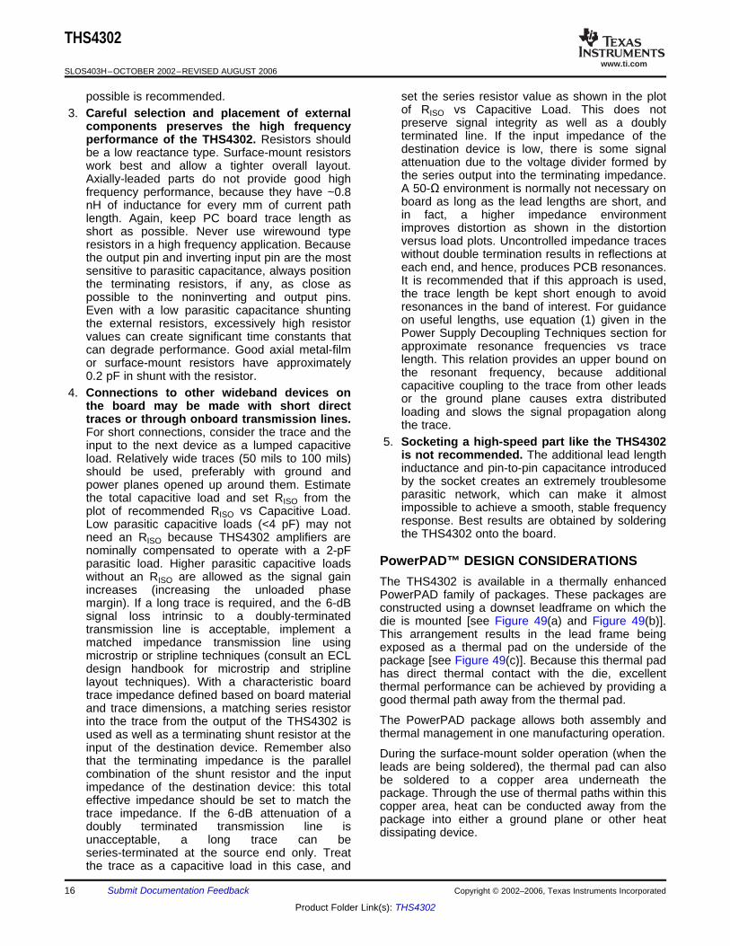
PowerPAD™ DESIGN CONSIDERATIONS
THS4302
SLOS403H–OCTOBER 2002–REVISED AUGUST 2006
possible is recommended. set the series resistor value as shown in the plotof RISO vs Capacitive Load. This does not3. Careful selection and placement of externalpreserve signal integrity as well as a doublycomponents preserves the high frequencyterminated line. If the input impedance of theperformance of the THS4302. Resistors shoulddestination device is low, there is some signalbe a low reactance type. Surface-mount resistorsattenuation due to the voltage divider formed bywork best and allow a tighter overall layout.the series output into the terminating impedance.Axially-leaded parts do not provide good highA 50-Ω environment is normally not necessary onfrequency performance, because they have ~0.8board as long as the lead lengths are short, andnH of inductance for every mm of current pathin fact, a higher impedance environmentlength. Again, keep PC board trace length asimproves distortion as shown in the distortionshort as possible. Never use wirewound typeversus load plots. Uncontrolled impedance tracesresistors in a high frequency application. Becausewithout double termination results in reflections atthe output pin and inverting input pin are the mosteach end, and hence, produces PCB resonances.sensitive to parasitic capacitance, always positionIt is recommended that if this approach is used,the terminating resistors, if any, as close asthe trace length be kept short enough to avoidpossible to the noninverting and output pins.resonances in the band of interest. For guidanceEven with a low parasitic capacitance shuntingon useful lengths, use equation (1) given in thethe external resistors, excessively high resistorPower Supply Decoupling Techniques section forvalues can create significant time constants thatapproximate resonance frequencies vs tracecan degrade performance. Good axial metal-filmlength. This relation provides an upper bound onor surface-mount resistors have approximatelythe resonant frequency, because additional0.2 pF in shunt with the resistor.capacitive coupling to the trace from other leads4. Connections to other wideband devices on or the ground plane causes extra distributedthe board may be made with short direct loading and slows the signal propagation alongtraces or through onboard transmission lines. the trace.For short connections, consider the trace and the
5. Socketing a high-speed part like the THS4302input to the next device as a lumped capacitiveis not recommended. The additional lead lengthload. Relatively wide traces (50 mils to 100 mils)inductance and pin-to-pin capacitance introducedshould be used, preferably with ground andby the socket creates an extremely troublesomepower planes opened up around them. Estimateparasitic network, which can make it almostthe total capacitive load and set RISO from theimpossible to achieve a smooth, stable frequencyplot of recommended RISO vs Capacitive Load.response. Best results are obtained by solderingLow parasitic capacitive loads (<4 pF) may notthe THS4302 onto the board.need an RISO because THS4302 amplifiers are
nominally compensated to operate with a 2-pFparasitic load. Higher parasitic capacitive loadswithout an RISO are allowed as the signal gain The THS4302 is available in a thermally enhancedincreases (increasing the unloaded phase PowerPAD family of packages. These packages aremargin). If a long trace is required, and the 6-dB constructed using a downset leadframe on which thesignal loss intrinsic to a doubly-terminated die is mounted [see Figure 49(a) and Figure 49(b)].transmission line is acceptable, implement a This arrangement results in the lead frame beingmatched impedance transmission line using exposed as a thermal pad on the underside of themicrostrip or stripline techniques (consult an ECL package [see Figure 49(c)]. Because this thermal paddesign handbook for microstrip and stripline has direct thermal contact with the die, excellentlayout techniques). With a characteristic board thermal performance can be achieved by providing atrace impedance defined based on board material good thermal path away from the thermal pad.and trace dimensions, a matching series resistor
The PowerPAD package allows both assembly andinto the trace from the output of the THS4302 isthermal management in one manufacturing operation.used as well as a terminating shunt resistor at the
input of the destination device. Remember also During the surface-mount solder operation (when thethat the terminating impedance is the parallel leads are being soldered), the thermal pad can alsocombination of the shunt resistor and the input be soldered to a copper area underneath theimpedance of the destination device: this total package. Through the use of thermal paths within thiseffective impedance should be set to match the copper area, heat can be conducted away from thetrace impedance. If the 6-dB attenuation of a package into either a ground plane or other heatdoubly terminated transmission line is dissipating device.unacceptable, a long trace can beseries-terminated at the source end only. Treatthe trace as a capacitive load in this case, and
16 Submit Documentation Feedback Copyright © 2002–2006, Texas Instruments Incorporated
Product Folder Link(s): THS4302
www.ti.com
DIE
Side View (a)
DIE
End View (b) Bottom View (c)
0.144 0.0195
0.144
0.010vias
Pin 1
Top View
0.012
0.030
0.07050.015
0.0095
0.049
0.032
0.0245
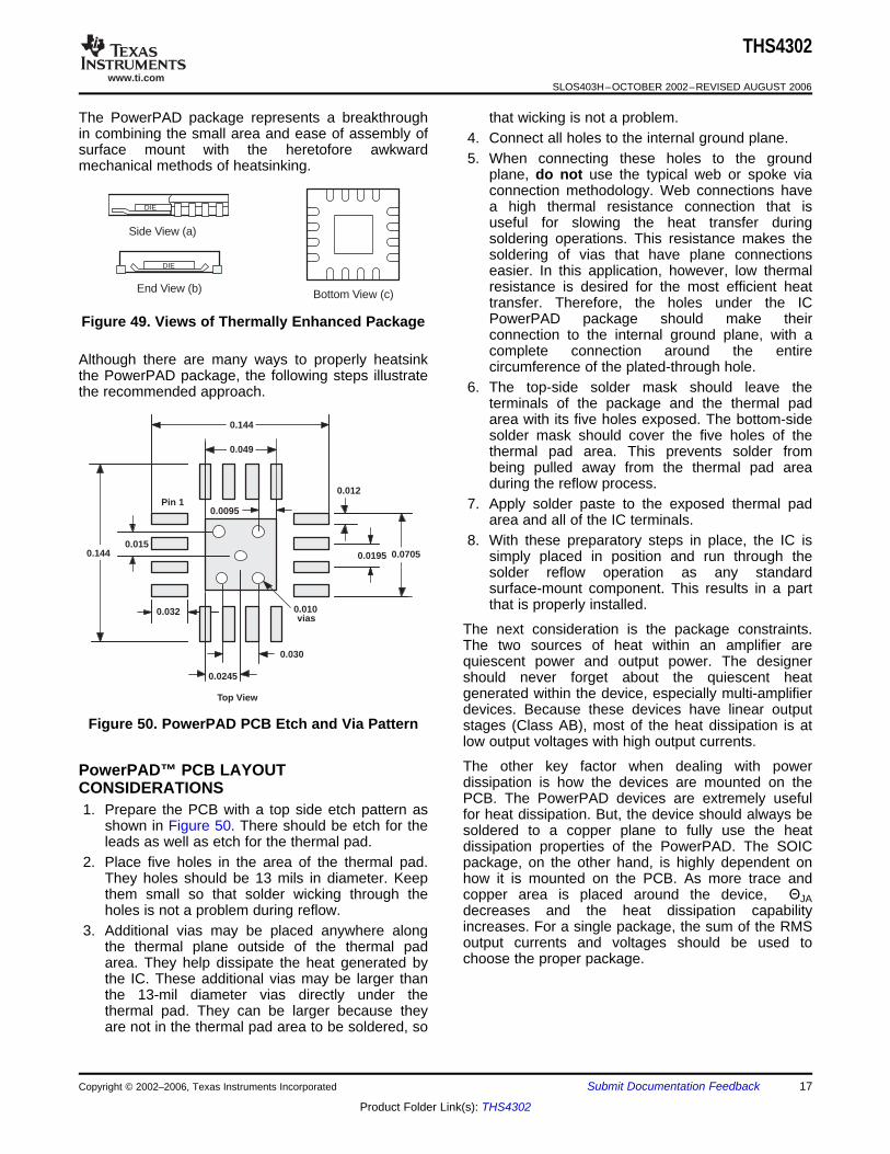
PowerPAD™ PCB LAYOUT
THS4302
SLOS403H–OCTOBER 2002–REVISED AUGUST 2006
The PowerPAD package represents a breakthrough that wicking is not a problem.in combining the small area and ease of assembly of 4. Connect all holes to the internal ground plane.surface mount with the heretofore awkward 5. When connecting these holes to the groundmechanical methods of heatsinking. plane, do not use the typical web or spoke via
connection methodology. Web connections havea high thermal resistance connection that isuseful for slowing the heat transfer duringsoldering operations. This resistance makes thesoldering of vias that have plane connectionseasier. In this application, however, low thermalresistance is desired for the most efficient heattransfer. Therefore, the holes under the ICPowerPAD package should make theirFigure 49. Views of Thermally Enhanced Packageconnection to the internal ground plane, with acomplete connection around the entireAlthough there are many ways to properly heatsink circumference of the plated-through hole.the PowerPAD package, the following steps illustrate
6. The top-side solder mask should leave thethe recommended approach.terminals of the package and the thermal padarea with its five holes exposed. The bottom-sidesolder mask should cover the five holes of thethermal pad area. This prevents solder frombeing pulled away from the thermal pad areaduring the reflow process.
7. Apply solder paste to the exposed thermal padarea and all of the IC terminals.
8. With these preparatory steps in place, the IC issimply placed in position and run through thesolder reflow operation as any standardsurface-mount component. This results in a partthat is properly installed.
The next consideration is the package constraints.The two sources of heat within an amplifier arequiescent power and output power. The designershould never forget about the quiescent heatgenerated within the device, especially multi-amplifierdevices. Because these devices have linear output
Figure 50. PowerPAD PCB Etch and Via Pattern stages (Class AB), most of the heat dissipation is atlow output voltages with high output currents.
The other key factor when dealing with powerdissipation is how the devices are mounted on theCONSIDERATIONSPCB. The PowerPAD devices are extremely useful
1. Prepare the PCB with a top side etch pattern as for heat dissipation. But, the device should always beshown in Figure 50. There should be etch for the soldered to a copper plane to fully use the heatleads as well as etch for the thermal pad. dissipation properties of the PowerPAD. The SOIC
2. Place five holes in the area of the thermal pad. package, on the other hand, is highly dependent onThey holes should be 13 mils in diameter. Keep how it is mounted on the PCB. As more trace andthem small so that solder wicking through the copper area is placed around the device, ΘJAholes is not a problem during reflow. decreases and the heat dissipation capability
increases. For a single package, the sum of the RMS3. Additional vias may be placed anywhere alongoutput currents and voltages should be used tothe thermal plane outside of the thermal padchoose the proper package.area. They help dissipate the heat generated by
the IC. These additional vias may be larger thanthe 13-mil diameter vias directly under thethermal pad. They can be larger because theyare not in the thermal pad area to be soldered, so
Copyright © 2002–2006, Texas Instruments Incorporated Submit Documentation Feedback 17
Product Folder Link(s): THS4302
www.ti.com
THERMAL ANALYSIS
DESIGN TOOLS
Evaluation Fixtures and Application Support
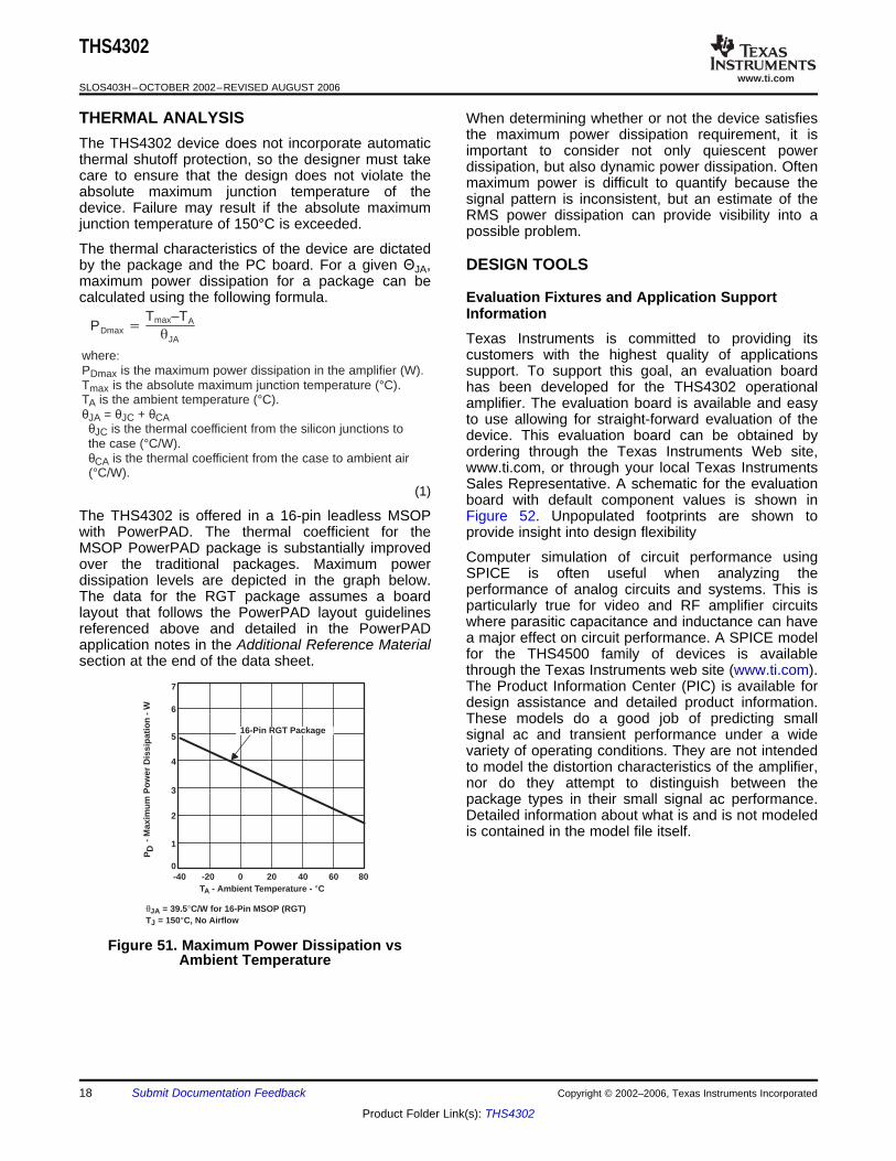
PDmaxTmax–TA
JA
where:PDmax is the maximum power dissipation in the amplifier (W).Tmax is the absolute maximum junction temperature (°C).TA is the ambient temperature (°C).θJA = θJC + θCA θJC is the thermal coefficient from the silicon junctions to the case (°C/W). θCA is the thermal coefficient from the case to ambient air (°C/W).
4
3
2
0-40 -20 0 20
- M
axim
um
Po
wer
Dis
sip
atio
n -
W
5
6
7
40 60 80TA - Ambient Temperature - °C
PD
16-Pin RGT Package
θJA = 39.5°C/W for 16-Pin MSOP (RGT)TJ = 150°C, No Airflow
1
THS4302
SLOS403H–OCTOBER 2002–REVISED AUGUST 2006
When determining whether or not the device satisfiesthe maximum power dissipation requirement, it isThe THS4302 device does not incorporate automatic important to consider not only quiescent powerthermal shutoff protection, so the designer must take dissipation, but also dynamic power dissipation. Oftencare to ensure that the design does not violate the maximum power is difficult to quantify because theabsolute maximum junction temperature of the signal pattern is inconsistent, but an estimate of thedevice. Failure may result if the absolute maximum RMS power dissipation can provide visibility into ajunction temperature of 150°C is exceeded. possible problem.
The thermal characteristics of the device are dictatedby the package and the PC board. For a given ΘJA,maximum power dissipation for a package can becalculated using the following formula.
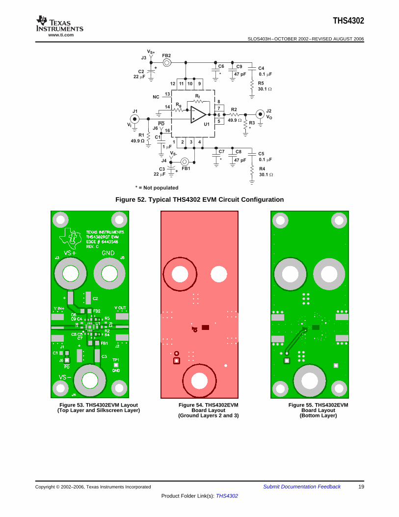
InformationTexas Instruments is committed to providing itscustomers with the highest quality of applicationssupport. To support this goal, an evaluation boardhas been developed for the THS4302 operationalamplifier. The evaluation board is available and easyto use allowing for straight-forward evaluation of thedevice. This evaluation board can be obtained byordering through the Texas Instruments Web site,www.ti.com, or through your local Texas InstrumentsSales Representative. A schematic for the evaluation(1) board with default component values is shown in
The THS4302 is offered in a 16-pin leadless MSOP Figure 52. Unpopulated footprints are shown towith PowerPAD. The thermal coefficient for the provide insight into design flexibilityMSOP PowerPAD package is substantially improved Computer simulation of circuit performance usingover the traditional packages. Maximum power SPICE is often useful when analyzing thedissipation levels are depicted in the graph below. performance of analog circuits and systems. This isThe data for the RGT package assumes a board particularly true for video and RF amplifier circuitslayout that follows the PowerPAD layout guidelines where parasitic capacitance and inductance can havereferenced above and detailed in the PowerPAD a major effect on circuit performance. A SPICE modelapplication notes in the Additional Reference Material for the THS4500 family of devices is availablesection at the end of the data sheet. through the Texas Instruments web site (www.ti.com).
The Product Information Center (PIC) is available fordesign assistance and detailed product information.These models do a good job of predicting smallsignal ac and transient performance under a widevariety of operating conditions. They are not intendedto model the distortion characteristics of the amplifier,nor do they attempt to distinguish between thepackage types in their small signal ac performance.Detailed information about what is and is not modeledis contained in the model file itself.
Figure 51. Maximum Power Dissipation vsAmbient Temperature
18 Submit Documentation Feedback Copyright © 2002–2006, Texas Instruments Incorporated
Product Folder Link(s): THS4302
www.ti.com
R1
49.9 Ω
_
+
Rf
VI
Rg8
7
6
5
R2
49.9 WR3
*
J2
VO
U1
1 2 3 4
+22 mF
NC
C3 FB1
*
C7
47 pF
C8 C5
0.1 mF
R4
30.1 W
11 10 912
J4
VS-
+
22 Fm*
C6
47 pF
C9 C4
0.1 mF
R5
30.1 W
FB2VS+
J3
14
13
16
PD
1 mF
C1
J1
J6
* = Not populated
C2
THS4302
SLOS403H–OCTOBER 2002–REVISED AUGUST 2006
Figure 52. Typical THS4302 EVM Circuit Configuration
Figure 53. THS4302EVM Layout Figure 54. THS4302EVM Figure 55. THS4302EVM(Top Layer and Silkscreen Layer) Board Layout Board Layout
(Ground Layers 2 and 3) (Bottom Layer)
Copyright © 2002–2006, Texas Instruments Incorporated Submit Documentation Feedback 19
Product Folder Link(s): THS4302
www.ti.com
ADDITIONAL REFERENCE MATERIAL
THS4302
SLOS403H–OCTOBER 2002–REVISED AUGUST 2006
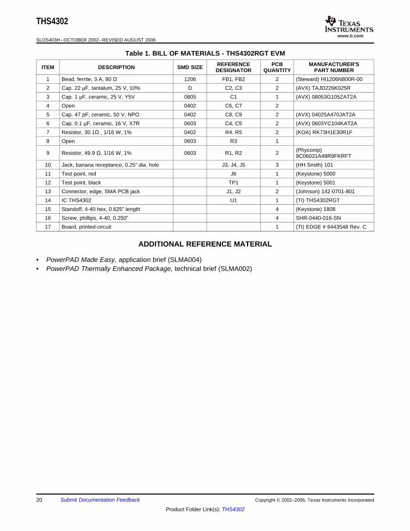
Table 1. BILL OF MATERIALS - THS4302RGT EVMREFERENCE PCB MANUFACTURER'SITEM DESCRIPTION SMD SIZE DESIGNATOR QUANTITY PART NUMBER
1 Bead, ferrite, 3 A, 80 Ω 1206 FB1, FB2 2 (Steward) HI1206N800R-002 Cap. 22 μF, tantalum, 25 V, 10% D C2, C3 2 (AVX) TAJD226K025R3 Cap. 1 μF, ceramic, 25 V, Y5V 0805 C1 1 (AVX) 08053G105ZAT2A4 Open 0402 C6, C7 25 Cap. 47 pF, ceramic, 50 V, NPO 0402 C8, C9 2 (AVX) 04025A470JAT2A6 Cap. 0.1 μF, ceramic, 16 V, X7R 0603 C4, C5 2 (AVX) 0603YC104KAT2A7 Resistor, 30.1Ω , 1/16 W, 1% 0402 R4, R5 2 (KOA) RK73H1E30R1F8 Open 0603 R3 1
(Phycomp)9 Resistor, 49.9 Ω, 1/16 W, 1% 0603 R1, R2 2 9C06031A49R9FKRFT10 Jack, banana receptance, 0.25” dia. hole J3, J4, J5 3 (HH Smith) 10111 Test point, red J6 1 (Keystone) 500012 Test point, black TP1 1 (Keystone) 500113 Connector, edge, SMA PCB jack J1, J2 2 (Johnson) 142-0701-80114 IC THS4302 U1 1 (TI) THS4302RGT15 Standoff, 4-40 hex, 0.625” length 4 (Keystone) 180816 Screw, phillips, 4-40, 0.250” 4 SHR-0440-016-SN17 Board, printed-circuit 1 (TI) EDGE # 6443548 Rev. C
• PowerPAD Made Easy, application brief (SLMA004)• PowerPAD Thermally Enhanced Package, technical brief (SLMA002)
20 Submit Documentation Feedback Copyright © 2002–2006, Texas Instruments Incorporated
Product Folder Link(s): THS4302
PACKAGE OPTION ADDENDUM
www.ti.com 11-Aug-2017
Addendum-Page 1
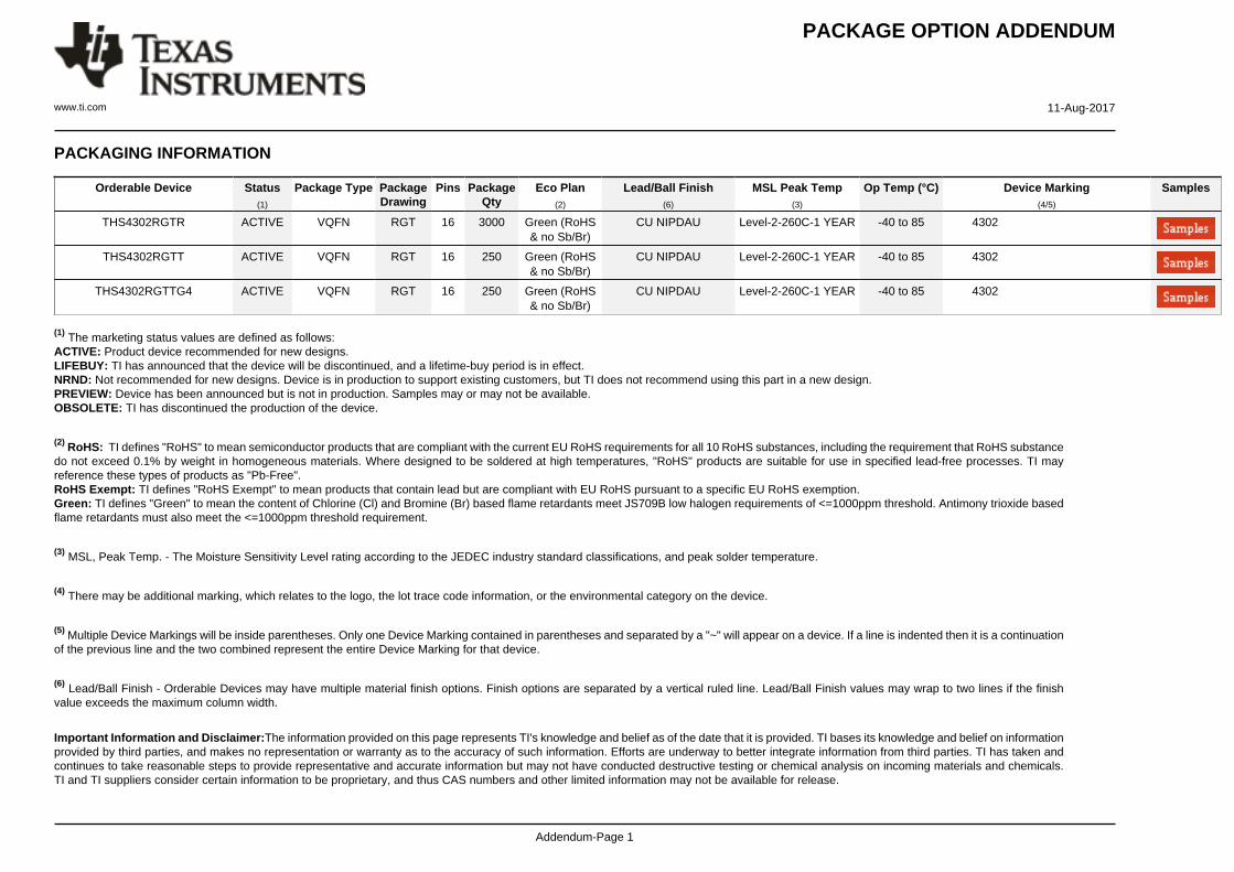
PACKAGING INFORMATION
Orderable Device Status(1)
Package Type PackageDrawing
Pins PackageQty
Eco Plan(2)
Lead/Ball Finish(6)
MSL Peak Temp(3)
Op Temp (°C) Device Marking(4/5)
Samples
THS4302RGTR ACTIVE VQFN RGT 16 3000 Green (RoHS& no Sb/Br)
CU NIPDAU Level-2-260C-1 YEAR -40 to 85 4302
THS4302RGTT ACTIVE VQFN RGT 16 250 Green (RoHS& no Sb/Br)
CU NIPDAU Level-2-260C-1 YEAR -40 to 85 4302
THS4302RGTTG4 ACTIVE VQFN RGT 16 250 Green (RoHS& no Sb/Br)
CU NIPDAU Level-2-260C-1 YEAR -40 to 85 4302
(1) The marketing status values are defined as follows:ACTIVE: Product device recommended for new designs.LIFEBUY: TI has announced that the device will be discontinued, and a lifetime-buy period is in effect.NRND: Not recommended for new designs. Device is in production to support existing customers, but TI does not recommend using this part in a new design.PREVIEW: Device has been announced but is not in production. Samples may or may not be available.OBSOLETE: TI has discontinued the production of the device.
(2) RoHS: TI defines "RoHS" to mean semiconductor products that are compliant with the current EU RoHS requirements for all 10 RoHS substances, including the requirement that RoHS substancedo not exceed 0.1% by weight in homogeneous materials. Where designed to be soldered at high temperatures, "RoHS" products are suitable for use in specified lead-free processes. TI mayreference these types of products as "Pb-Free".RoHS Exempt: TI defines "RoHS Exempt" to mean products that contain lead but are compliant with EU RoHS pursuant to a specific EU RoHS exemption.Green: TI defines "Green" to mean the content of Chlorine (Cl) and Bromine (Br) based flame retardants meet JS709B low halogen requirements of <=1000ppm threshold. Antimony trioxide basedflame retardants must also meet the <=1000ppm threshold requirement.
(3) MSL, Peak Temp. - The Moisture Sensitivity Level rating according to the JEDEC industry standard classifications, and peak solder temperature.
(4) There may be additional marking, which relates to the logo, the lot trace code information, or the environmental category on the device.
(5) Multiple Device Markings will be inside parentheses. Only one Device Marking contained in parentheses and separated by a "~" will appear on a device. If a line is indented then it is a continuationof the previous line and the two combined represent the entire Device Marking for that device.
(6) Lead/Ball Finish - Orderable Devices may have multiple material finish options. Finish options are separated by a vertical ruled line. Lead/Ball Finish values may wrap to two lines if the finishvalue exceeds the maximum column width.
Important Information and Disclaimer:The information provided on this page represents TI's knowledge and belief as of the date that it is provided. TI bases its knowledge and belief on informationprovided by third parties, and makes no representation or warranty as to the accuracy of such information. Efforts are underway to better integrate information from third parties. TI has taken andcontinues to take reasonable steps to provide representative and accurate information but may not have conducted destructive testing or chemical analysis on incoming materials and chemicals.TI and TI suppliers consider certain information to be proprietary, and thus CAS numbers and other limited information may not be available for release.
PACKAGE OPTION ADDENDUM
www.ti.com 11-Aug-2017
Addendum-Page 2
In no event shall TI's liability arising out of such information exceed the total purchase price of the TI part(s) at issue in this document sold by TI to Customer on an annual basis.
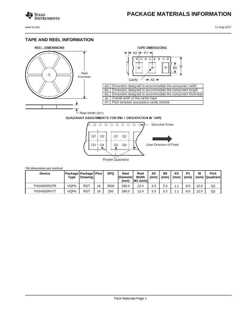
TAPE AND REEL INFORMATION
*All dimensions are nominal
Device PackageType
PackageDrawing
Pins SPQ ReelDiameter
(mm)
ReelWidth
W1 (mm)
A0(mm)
B0(mm)
K0(mm)
P1(mm)
W(mm)
Pin1Quadrant
THS4302RGTR VQFN RGT 16 3000 330.0 12.4 3.3 3.3 1.1 8.0 12.0 Q2
THS4302RGTT VQFN RGT 16 250 180.0 12.4 3.3 3.3 1.1 8.0 12.0 Q2
PACKAGE MATERIALS INFORMATION
www.ti.com 11-Aug-2017
Pack Materials-Page 1
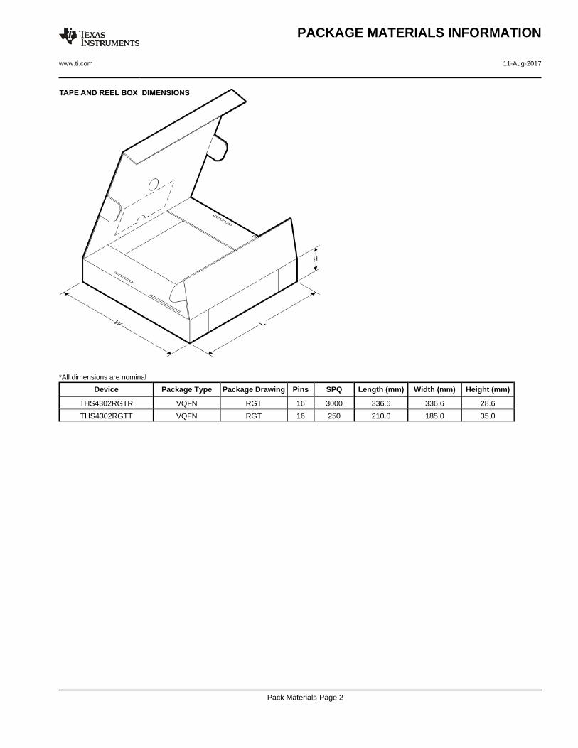
*All dimensions are nominal
Device Package Type Package Drawing Pins SPQ Length (mm) Width (mm) Height (mm)
THS4302RGTR VQFN RGT 16 3000 336.6 336.6 28.6
THS4302RGTT VQFN RGT 16 250 210.0 185.0 35.0
PACKAGE MATERIALS INFORMATION
www.ti.com 11-Aug-2017
Pack Materials-Page 2
www.ti.com
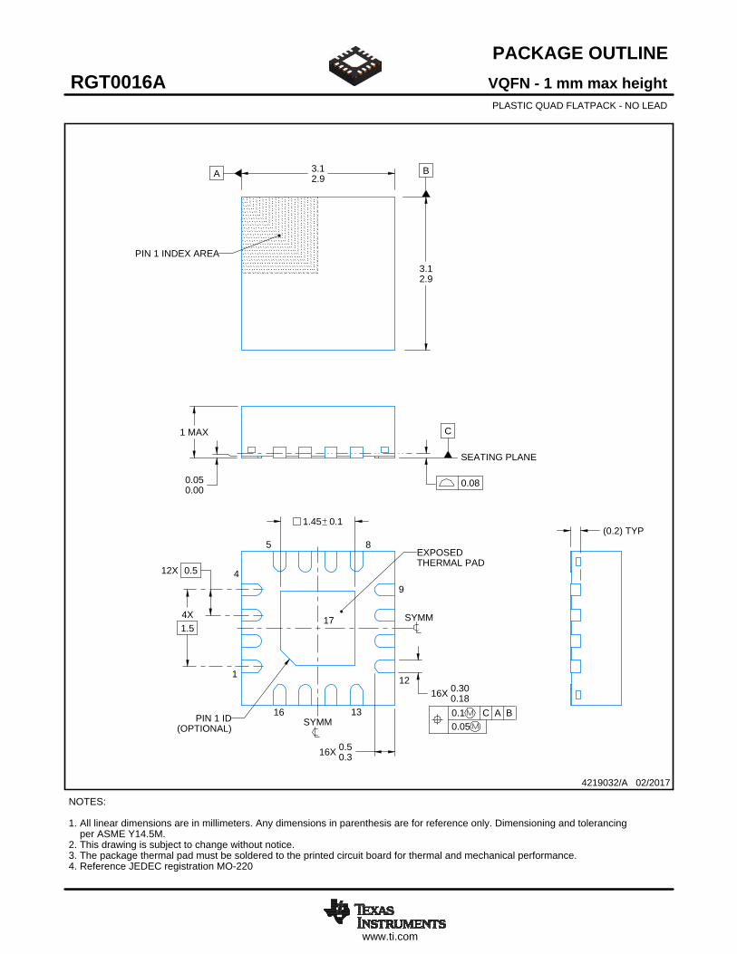
PACKAGE OUTLINE
C
16X 0.300.18
1.45 0.1
16X 0.50.3
1 MAX
(0.2) TYP
0.050.00
12X 0.5
4X1.5
A 3.12.9
B
3.12.9
VQFN - 1 mm max heightRGT0016APLASTIC QUAD FLATPACK - NO LEAD
4219032/A 02/2017
PIN 1 INDEX AREA
0.08
SEATING PLANE
1
49
12
5 8
16 13
(OPTIONAL)PIN 1 ID 0.1 C A B
0.05
EXPOSEDTHERMAL PAD
SYMM
SYMM
17
NOTES: 1. All linear dimensions are in millimeters. Any dimensions in parenthesis are for reference only. Dimensioning and tolerancing per ASME Y14.5M. 2. This drawing is subject to change without notice. 3. The package thermal pad must be soldered to the printed circuit board for thermal and mechanical performance.4. Reference JEDEC registration MO-220
SCALE 3.600
www.ti.com
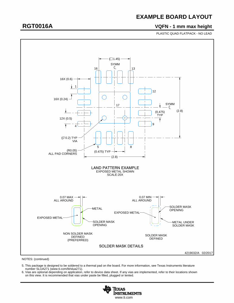
EXAMPLE BOARD LAYOUT
0.07 MINALL AROUND
0.07 MAXALL AROUND
16X (0.24)
16X (0.6)
( 0.2) TYPVIA
12X (0.5)
(2.8)
(2.8)
(0.475)TYP
( 1.45)
(R0.05)ALL PAD CORNERS
(0.475) TYP
VQFN - 1 mm max heightRGT0016APLASTIC QUAD FLATPACK - NO LEAD
4219032/A 02/2017
SYMM
1
4
5 8
9
12
1316
SYMM
LAND PATTERN EXAMPLEEXPOSED METAL SHOWN
SCALE:20X
17
NOTES: (continued) 5. This package is designed to be soldered to a thermal pad on the board. For more information, see Texas Instruments literature number SLUA271 (www.ti.com/lit/slua271).6. Vias are optional depending on application, refer to device data sheet. If any vias are implemented, refer to their locations shown on this view. It is recommended that vias under paste be filled, plugged or tented.
SOLDER MASKOPENING
METAL UNDERSOLDER MASK
SOLDER MASKDEFINED
EXPOSED METALMETAL
SOLDER MASKOPENING
SOLDER MASK DETAILS
NON SOLDER MASKDEFINED
(PREFERRED)
EXPOSED METAL
www.ti.com
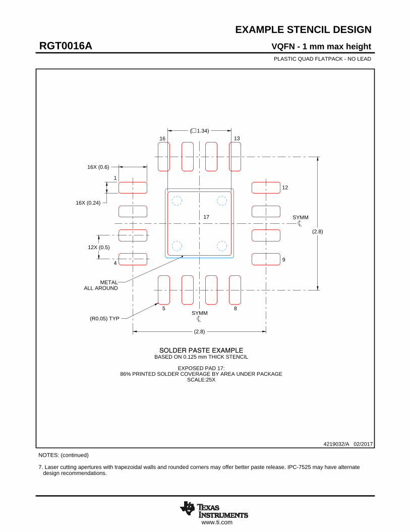
EXAMPLE STENCIL DESIGN
16X (0.6)
16X (0.24)
12X (0.5)
(2.8)
(2.8)
( 1.34)
(R0.05) TYP
VQFN - 1 mm max heightRGT0016APLASTIC QUAD FLATPACK - NO LEAD
4219032/A 02/2017
NOTES: (continued) 7. Laser cutting apertures with trapezoidal walls and rounded corners may offer better paste release. IPC-7525 may have alternate design recommendations.
SYMM
ALL AROUNDMETAL
SOLDER PASTE EXAMPLEBASED ON 0.125 mm THICK STENCIL
EXPOSED PAD 17:
86% PRINTED SOLDER COVERAGE BY AREA UNDER PACKAGESCALE:25X
SYMM
1
4
5 8
9
12
1316
17
IMPORTANT NOTICE
Texas Instruments Incorporated (TI) reserves the right to make corrections, enhancements, improvements and other changes to itssemiconductor products and services per JESD46, latest issue, and to discontinue any product or service per JESD48, latest issue. Buyersshould obtain the latest relevant information before placing orders and should verify that such information is current and complete.TI’s published terms of sale for semiconductor products (http://www.ti.com/sc/docs/stdterms.htm) apply to the sale of packaged integratedcircuit products that TI has qualified and released to market. Additional terms may apply to the use or sale of other types of TI products andservices.Reproduction of significant portions of TI information in TI data sheets is permissible only if reproduction is without alteration and isaccompanied by all associated warranties, conditions, limitations, and notices. TI is not responsible or liable for such reproduceddocumentation. Information of third parties may be subject to additional restrictions. Resale of TI products or services with statementsdifferent from or beyond the parameters stated by TI for that product or service voids all express and any implied warranties for theassociated TI product or service and is an unfair and deceptive business practice. TI is not responsible or liable for any such statements.Buyers and others who are developing systems that incorporate TI products (collectively, “Designers”) understand and agree that Designersremain responsible for using their independent analysis, evaluation and judgment in designing their applications and that Designers havefull and exclusive responsibility to assure the safety of Designers' applications and compliance of their applications (and of all TI productsused in or for Designers’ applications) with all applicable regulations, laws and other applicable requirements. Designer represents that, withrespect to their applications, Designer has all the necessary expertise to create and implement safeguards that (1) anticipate dangerousconsequences of failures, (2) monitor failures and their consequences, and (3) lessen the likelihood of failures that might cause harm andtake appropriate actions. Designer agrees that prior to using or distributing any applications that include TI products, Designer willthoroughly test such applications and the functionality of such TI products as used in such applications.TI’s provision of technical, application or other design advice, quality characterization, reliability data or other services or information,including, but not limited to, reference designs and materials relating to evaluation modules, (collectively, “TI Resources”) are intended toassist designers who are developing applications that incorporate TI products; by downloading, accessing or using TI Resources in anyway, Designer (individually or, if Designer is acting on behalf of a company, Designer’s company) agrees to use any particular TI Resourcesolely for this purpose and subject to the terms of this Notice.TI’s provision of TI Resources does not expand or otherwise alter TI’s applicable published warranties or warranty disclaimers for TIproducts, and no additional obligations or liabilities arise from TI providing such TI Resources. TI reserves the right to make corrections,enhancements, improvements and other changes to its TI Resources. TI has not conducted any testing other than that specificallydescribed in the published documentation for a particular TI Resource.Designer is authorized to use, copy and modify any individual TI Resource only in connection with the development of applications thatinclude the TI product(s) identified in such TI Resource. NO OTHER LICENSE, EXPRESS OR IMPLIED, BY ESTOPPEL OR OTHERWISETO ANY OTHER TI INTELLECTUAL PROPERTY RIGHT, AND NO LICENSE TO ANY TECHNOLOGY OR INTELLECTUAL PROPERTYRIGHT OF TI OR ANY THIRD PARTY IS GRANTED HEREIN, including but not limited to any patent right, copyright, mask work right, orother intellectual property right relating to any combination, machine, or process in which TI products or services are used. Informationregarding or referencing third-party products or services does not constitute a license to use such products or services, or a warranty orendorsement thereof. Use of TI Resources may require a license from a third party under the patents or other intellectual property of thethird party, or a license from TI under the patents or other intellectual property of TI.TI RESOURCES ARE PROVIDED “AS IS” AND WITH ALL FAULTS. TI DISCLAIMS ALL OTHER WARRANTIES ORREPRESENTATIONS, EXPRESS OR IMPLIED, REGARDING RESOURCES OR USE THEREOF, INCLUDING BUT NOT LIMITED TOACCURACY OR COMPLETENESS, TITLE, ANY EPIDEMIC FAILURE WARRANTY AND ANY IMPLIED WARRANTIES OFMERCHANTABILITY, FITNESS FOR A PARTICULAR PURPOSE, AND NON-INFRINGEMENT OF ANY THIRD PARTY INTELLECTUALPROPERTY RIGHTS. TI SHALL NOT BE LIABLE FOR AND SHALL NOT DEFEND OR INDEMNIFY DESIGNER AGAINST ANY CLAIM,INCLUDING BUT NOT LIMITED TO ANY INFRINGEMENT CLAIM THAT RELATES TO OR IS BASED ON ANY COMBINATION OFPRODUCTS EVEN IF DESCRIBED IN TI RESOURCES OR OTHERWISE. IN NO EVENT SHALL TI BE LIABLE FOR ANY ACTUAL,DIRECT, SPECIAL, COLLATERAL, INDIRECT, PUNITIVE, INCIDENTAL, CONSEQUENTIAL OR EXEMPLARY DAMAGES INCONNECTION WITH OR ARISING OUT OF TI RESOURCES OR USE THEREOF, AND REGARDLESS OF WHETHER TI HAS BEENADVISED OF THE POSSIBILITY OF SUCH DAMAGES.Unless TI has explicitly designated an individual product as meeting the requirements of a particular industry standard (e.g., ISO/TS 16949and ISO 26262), TI is not responsible for any failure to meet such industry standard requirements.Where TI specifically promotes products as facilitating functional safety or as compliant with industry functional safety standards, suchproducts are intended to help enable customers to design and create their own applications that meet applicable functional safety standardsand requirements. Using products in an application does not by itself establish any safety features in the application. Designers mustensure compliance with safety-related requirements and standards applicable to their applications. Designer may not use any TI products inlife-critical medical equipment unless authorized officers of the parties have executed a special contract specifically governing such use.Life-critical medical equipment is medical equipment where failure of such equipment would cause serious bodily injury or death (e.g., lifesupport, pacemakers, defibrillators, heart pumps, neurostimulators, and implantables). Such equipment includes, without limitation, allmedical devices identified by the U.S. Food and Drug Administration as Class III devices and equivalent classifications outside the U.S.TI may expressly designate certain products as completing a particular qualification (e.g., Q100, Military Grade, or Enhanced Product).Designers agree that it has the necessary expertise to select the product with the appropriate qualification designation for their applicationsand that proper product selection is at Designers’ own risk. Designers are solely responsible for compliance with all legal and regulatoryrequirements in connection with such selection.Designer will fully indemnify TI and its representatives against any damages, costs, losses, and/or liabilities arising out of Designer’s non-compliance with the terms and provisions of this Notice.
Mailing Address: Texas Instruments, Post Office Box 655303, Dallas, Texas 75265Copyright © 2017, Texas Instruments Incorporated


![Data Supply Inc. October 2016english).pdf · Data Supply Inc. October 2016 2016 version [Toner Market Forecast] Outlook for the Toner Industry that Will Continue to Strive for Excellence](https://static.fdocument.org/doc/165x107/5ebb3460ffbf2e3df7086339/data-supply-inc-october-englishpdf-data-supply-inc-october-2016-2016-version.jpg)


![[scale=.25]img/KTH.png *.5mm The origin and limitations of .../main.pdf · sinusoidal signals, i.e. E =Re E 1ejw1t +E 2ejw2t where w 1 = w a w 0 and w 2 = w a +w 0, that assures that](https://static.fdocument.org/doc/165x107/5c6a1e5409d3f27a7e8c27eb/scale25imgkthpng-5mm-the-origin-and-limitations-of-mainpdf-sinusoidal.jpg)