UCC25705, UCC25706, UCC35705, UCC35706 HIGH-SPEED … · ucc25705, ucc25706, ucc35705, ucc35706...
22
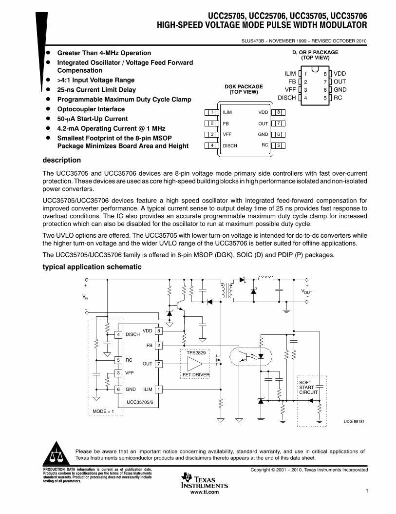
UCC25705, UCC25706, UCC35705, UCC35706 HIGH-SPEED VOLTAGE MODE PULSE WIDTH MODULATOR SLUS473B -- NOVEMBER 1999 -- REVISED OCTOBER 2010 1 www.ti.com D Greater Than 4-MHz Operation D Integrated Oscillator / Voltage Feed Forward Compensation D >4:1 Input Voltage Range D 25-ns Current Limit Delay D Programmable Maximum Duty Cycle Clamp D Optocoupler Interface D 50-μA Start-Up Current D 4.2-mA Operating Current @ 1 MHz D Smallest Footprint of the 8-pin MSOP Package Minimizes Board Area and Height description The UCC35705 and UCC35706 devices are 8-pin voltage mode primary side controllers with fast over-current protection. These devices are used as core high-speed building blocks in high performance isolated and non-isolated power converters. UCC35705/UCC35706 devices feature a high speed oscillator with integrated feed-forward compensation for improved converter performance. A typical current sense to output delay time of 25 ns provides fast response to overload conditions. The IC also provides an accurate programmable maximum duty cycle clamp for increased protection which can also be disabled for the oscillator to run at maximum possible duty cycle. Two UVLO options are offered. The UCC35705 with lower turn-on voltage is intended for dc-to-dc converters while the higher turn-on voltage and the wider UVLO range of the UCC35706 is better suited for offline applications. The UCC35705/UCC35706 family is offered in 8-pin MSOP (DGK), SOIC (D) and PDIP (P) packages. typical application schematic UDG-99181 VDD OUT GND RC ILIM VFF DISCH UCC35705/6 + -- V OUT + V IN SOFT START CIRCUIT 4 5 3 6 8 7 1 TPS2829 -- FB 2 MODE = 1 FET DRIVER Copyright © 2001 -- 2010, Texas Instruments Incorporated PRODUCTION DATA information is current as of publication date. Products conform to specifications per the terms of Texas Instruments standard warranty. Production processing does not necessarily include testing of all parameters. Please be aware that an important notice concerning availability, standard warranty, and use in critical applications of Texas Instruments semiconductor products and disclaimers thereto appears at the end of this data sheet. 1 2 3 4 8 7 6 5 ILIM FB VFF DISCH VDD OUT GND RC D, OR P PACKAGE (TOP VIEW) ILIM 2 1 4 3 7 8 5 6 FB VFF DISCH VDD OUT GND RC DGK PACKAGE (TOP VIEW)
Transcript of UCC25705, UCC25706, UCC35705, UCC35706 HIGH-SPEED … · ucc25705, ucc25706, ucc35705, ucc35706...
UCC25705, UCC25706, UCC35705, UCC35706HIGH-SPEED VOLTAGE MODE PULSE WIDTH MODULATOR
SLUS473B -- NOVEMBER 1999 -- REVISED OCTOBER 2010
1www.ti.com
D Greater Than 4-MHz OperationD Integrated Oscillator / Voltage Feed Forward
Compensation
D >4:1 Input Voltage Range
D 25-ns Current Limit DelayD Programmable Maximum Duty Cycle Clamp
D Optocoupler InterfaceD 50-μA Start-Up Current
D 4.2-mA Operating Current @ 1 MHzD Smallest Footprint of the 8-pin MSOP
Package Minimizes Board Area and Height
description
The UCC35705 and UCC35706 devices are 8-pin voltage mode primary side controllers with fast over-currentprotection. Thesedevices are usedas core high-speedbuilding blocks in high performance isolated andnon-isolatedpower converters.
UCC35705/UCC35706 devices feature a high speed oscillator with integrated feed-forward compensation forimproved converter performance. A typical current sense to output delay time of 25 ns provides fast response tooverload conditions. The IC also provides an accurate programmable maximum duty cycle clamp for increasedprotection which can also be disabled for the oscillator to run at maximum possible duty cycle.
Two UVLO options are offered. The UCC35705 with lower turn-on voltage is intended for dc-to-dc converters whilethe higher turn-on voltage and the wider UVLO range of the UCC35706 is better suited for offline applications.
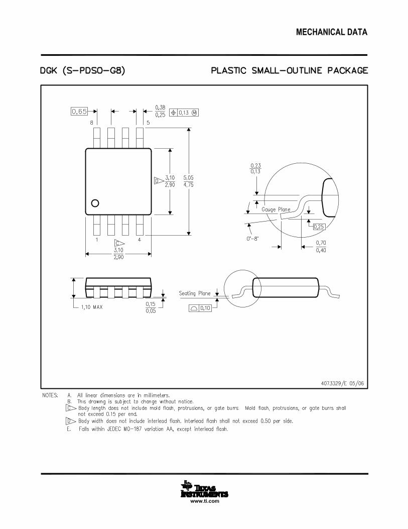
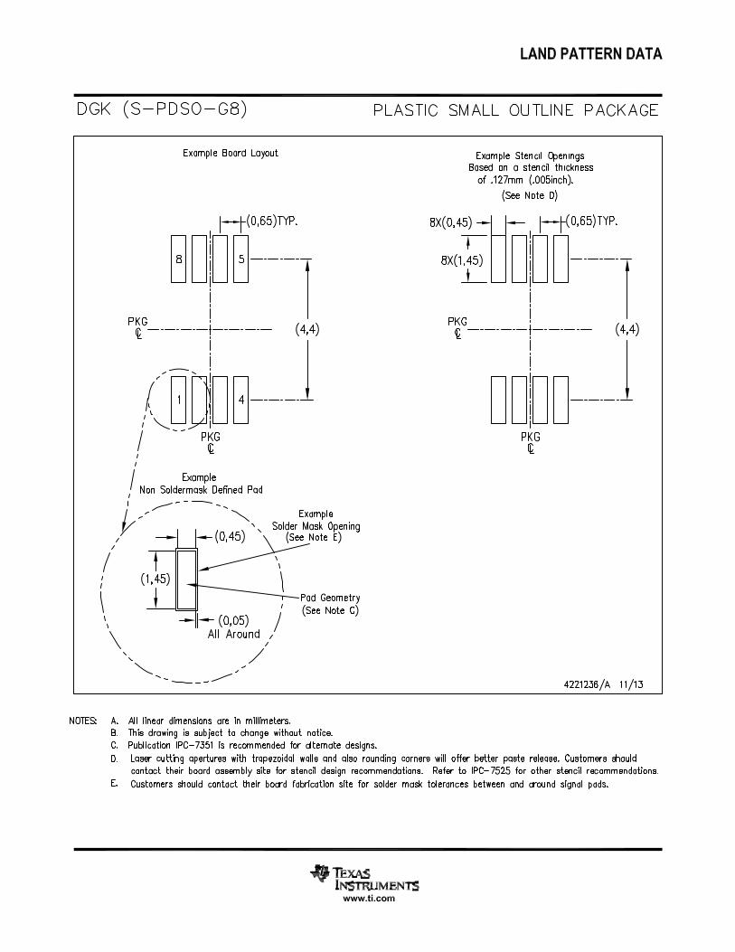
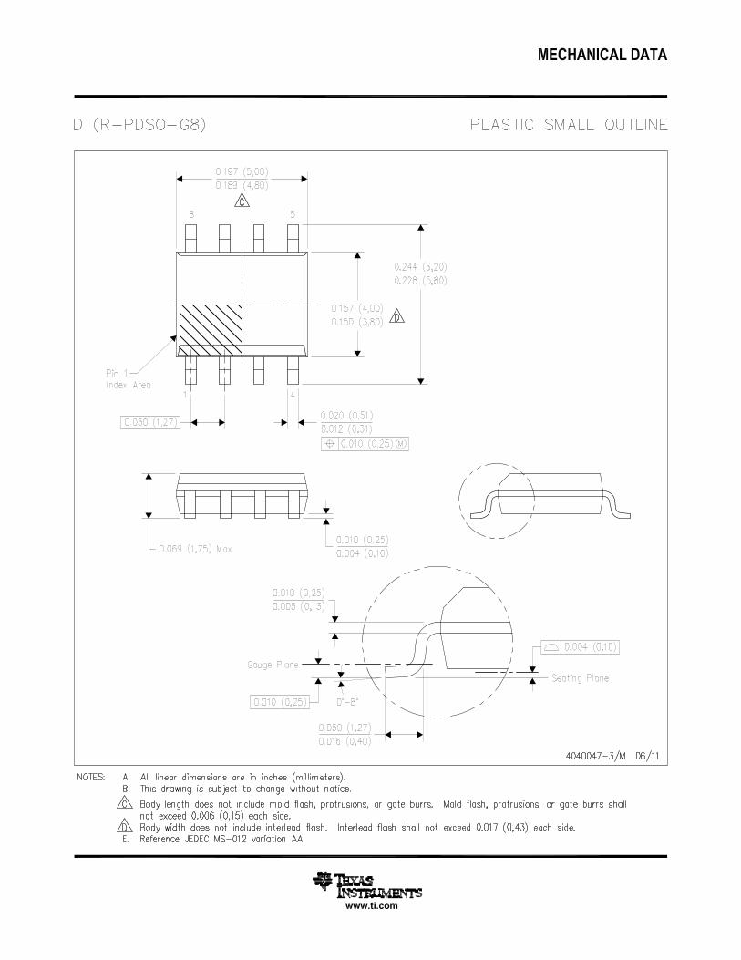
The UCC35705/UCC35706 family is offered in 8-pin MSOP (DGK), SOIC (D) and PDIP (P) packages.
typical application schematic
UDG-99181
VDD
OUT
GND
RC
ILIM
VFF
DISCH
UCC35705/6
+
--VOUT
+
VIN
SOFTSTARTCIRCUIT
4
5
3
6
8
7
1
TPS2829
--
FB 2
MODE = 1
FET DRIVER
Copyright © 2001 -- 2010, Texas Instruments IncorporatedPRODUCTION DATA information is current as of publication date.Products conform to specifications per the terms of Texas Instrumentsstandard warranty. Production processing does not necessarily includetesting of all parameters.
Please be aware that an important notice concerning availability, standard warranty, and use in critical applications ofTexas Instruments semiconductor products and disclaimers thereto appears at the end of this data sheet.
1
2
3
4
8
7
6
5
ILIMFB
VFFDISCH
VDDOUTGNDRC
D, OR P PACKAGE(TOP VIEW)
ILIM
2
1
4
3
7
8
5
6
FB
VFF
DISCH
VDD
OUT
GND
RC
DGK PACKAGE(TOP VIEW)
UCC25705, UCC25706, UCC35705, UCC35706HIGH-SPEED VOLTAGE MODE PULSE WIDTH MODULATOR
SLUS473B -- NOVEMBER 1999 -- REVISED OCTOBER 2010
2 www.ti.com
absolute maximum ratings over operating free-air temperature (unless otherwise noted)†
Supply voltage 15 V. . . . . . . . . . . . . . . . . . . . . . . . . . . . . . . . . . . . . . . . . . . . . . . . . . . . . . . . . . . . . . . . . . . . . . . . . . . .Input voltage (VFF,RC,ILIM) 7 V. . . . . . . . . . . . . . . . . . . . . . . . . . . . . . . . . . . . . . . . . . . . . . . . . . . . . . . . . . . . . . . . .Input voltage (FB) 15 V. . . . . . . . . . . . . . . . . . . . . . . . . . . . . . . . . . . . . . . . . . . . . . . . . . . . . . . . . . . . . . . . . . . . . . . . .Input current (DISCH) 1 mA. . . . . . . . . . . . . . . . . . . . . . . . . . . . . . . . . . . . . . . . . . . . . . . . . . . . . . . . . . . . . . . . . . . . . .Output current (OUT) dc ±20 mA. . . . . . . . . . . . . . . . . . . . . . . . . . . . . . . . . . . . . . . . . . . . . . . . . . . . . . . . . . . . . . . . .Storage temperature, Tstg –65°C to 150°C. . . . . . . . . . . . . . . . . . . . . . . . . . . . . . . . . . . . . . . . . . . . . . . . . . . . . . . . .Junction temperature, TJ –55°C to 150°C. . . . . . . . . . . . . . . . . . . . . . . . . . . . . . . . . . . . . . . . . . . . . . . . . . . . . . . . .Lead temperature (soldering, 10 sec.) 300°C. . . . . . . . . . . . . . . . . . . . . . . . . . . . . . . . . . . . . . . . . . . . . . . . . . . . . . .† Stresses beyond those listed under “absolutemaximum ratings”may cause permanent damage to the device. These are stress ratings only, andfunctional operation of the device at these or any other conditions beyond those indicated under “recommended operating conditions” is notimplied. Exposure to absolute-maximum-rated conditions for extended periods may affect device reliability.
‡ All voltages are with respect to GND. Currents are positive into, negative out of the specified terminal. Consult Packaging Section of the PowerSupply Control Data Book (TI Literature Number SLUD003) for thermal limitations and considerations of packages.
AVAILABLE OPTIONS
Packaged Devices
TA = TJUVLO Option
SOIC-8Small Outline (D)†
PDIP-8Plastic Dip (P)
MSOP-8Small Outline
(DGK)†
--40°C to 85°C8.8V/8V UCC25705D UCC25705P UCC25705DGK
--40°C to 85°C12V/8V UCC25706D UCC25706P UCC25706DGK
0°C to 70°C8.8V/8V UCC35705D UCC35705P UCC35705DGK
0°C to 70°C12V/8V UCC35706D UCC35706P UCC35706DGK
† D (SOIC--8) and DGK (MSOP--8) packages are available taped and reeled. Add R suffix to device type (e.g.UCC35705DR) to order quantities of 2500 devices per reel for SOIC-8 and 2000 devices per reel for the MSOP-8.
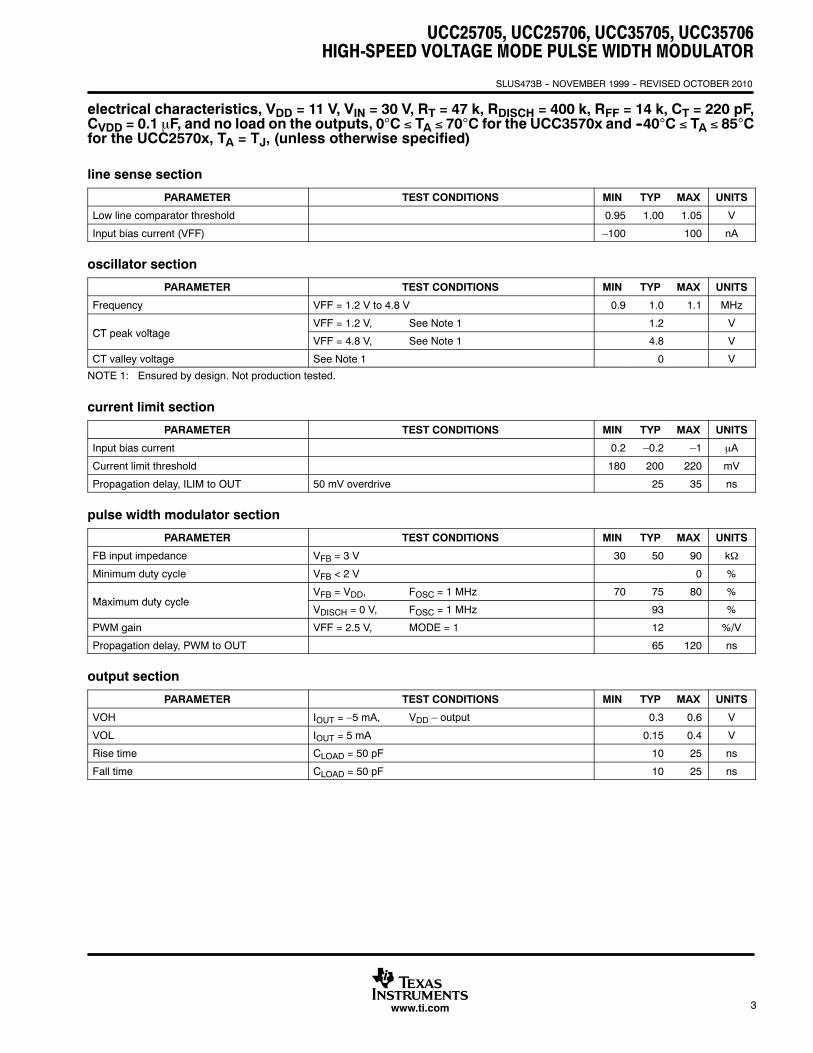
electrical characteristics, VDD = 11 V, VIN = 30 V, RT = 47 k, RDISCH = 400 k, RFF = 14 k, CT = 220 pF,CVDD = 0.1 μF, and no load on the outputs, 0°C ≤ TA ≤ 70°C for the UCC3570x and --40°C ≤ TA ≤ 85°Cfor the UCC2570x, TA = TJ, (unless otherwise specified)
UVLO section (UCCx5705)
PARAMETER TEST CONDITIONS MIN TYP MAX UNITS
Start threshold 8.0 8.8 9.6 V
Stop threshold 7.4 8.2 9.0 V
Hysteresis 0.3 0.6 1.0 V
UVLO section (UCCx5706)
PARAMETER TEST CONDITIONS MIN TYP MAX UNITS
Start threshold 11.2 12.0 12.8 V
Stop threshold 7.2 8.0 8.8 V
Hysteresis 3.5 4.0 4.5 V
supply current section
PARAMETER TEST CONDITIONS MIN TYP MAX UNITS
Start-up current VDD = UVLO start – 1 V, VDD comparator off 30 90 μA
IDD active VDD comparator on, oscillator running at 1 MHz 4.2 5.0 mA
UCC25705, UCC25706, UCC35705, UCC35706HIGH-SPEED VOLTAGE MODE PULSE WIDTH MODULATOR
SLUS473B -- NOVEMBER 1999 -- REVISED OCTOBER 2010
3www.ti.com
electrical characteristics, VDD = 11 V, VIN = 30 V, RT = 47 k, RDISCH = 400 k, RFF = 14 k, CT = 220 pF,CVDD = 0.1 μF, and no load on the outputs, 0°C ≤ TA ≤ 70°C for the UCC3570x and --40°C ≤ TA ≤ 85°Cfor the UCC2570x, TA = TJ, (unless otherwise specified)
line sense section
PARAMETER TEST CONDITIONS MIN TYP MAX UNITS
Low line comparator threshold 0.95 1.00 1.05 V
Input bias current (VFF) –100 100 nA
oscillator section
PARAMETER TEST CONDITIONS MIN TYP MAX UNITS
Frequency VFF = 1.2 V to 4.8 V 0.9 1.0 1.1 MHz
CT peak voltageVFF = 1.2 V, See Note 1 1.2 V
CT peak voltageVFF = 4.8 V, See Note 1 4.8 V
CT valley voltage See Note 1 0 V
NOTE 1: Ensured by design. Not production tested.
current limit section
PARAMETER TEST CONDITIONS MIN TYP MAX UNITS
Input bias current 0.2 –0.2 –1 μA
Current limit threshold 180 200 220 mV
Propagation delay, ILIM to OUT 50 mV overdrive 25 35 ns
pulse width modulator section
PARAMETER TEST CONDITIONS MIN TYP MAX UNITS
FB input impedance VFB = 3 V 30 50 90 kΩ
Minimum duty cycle VFB < 2 V 0 %
Ma im m d t c cleVFB = VDD, FOSC = 1 MHz 70 75 80 %
Maximum duty cycleVDISCH = 0 V, FOSC = 1 MHz 93 %
PWM gain VFF = 2.5 V, MODE = 1 12 %/V
Propagation delay, PWM to OUT 65 120 ns
output section
PARAMETER TEST CONDITIONS MIN TYP MAX UNITS
VOH IOUT = –5 mA, VDD – output 0.3 0.6 V
VOL IOUT = 5 mA 0.15 0.4 V
Rise time CLOAD = 50 pF 10 25 ns
Fall time CLOAD = 50 pF 10 25 ns
UCC25705, UCC25706, UCC35705, UCC35706HIGH-SPEED VOLTAGE MODE PULSE WIDTH MODULATOR
SLUS473B -- NOVEMBER 1999 -- REVISED OCTOBER 2010
4 www.ti.com
pin descriptions
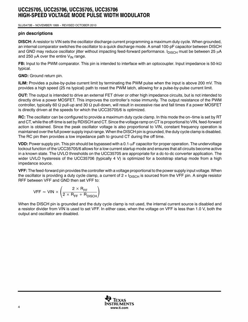
DISCH:A resistor to VIN sets the oscillator discharge current programming amaximum duty cycle.When grounded,an internal comparator switches the oscillator to a quick discharge mode. A small 100-pF capacitor between DISCHand GND may reduce oscillator jitter without impacting feed-forward performance. IDISCH must be between 25 μAand 250 μA over the entire VIN range.
FB: Input to the PWM comparator. This pin is intended to interface with an optocoupler. Input impedance is 50-kΩtypical.
GND: Ground return pin.
ILIM: Provides a pulse-by-pulse current limit by terminating the PWM pulse when the input is above 200 mV. Thisprovides a high speed (25 ns typical) path to reset the PWM latch, allowing for a pulse-by-pulse current limit.
OUT: The output is intended to drive an external FET driver or other high impedance circuits, but is not intended todirectly drive a power MOSFET. This improves the controller’s noise immunity. The output resistance of the PWMcontroller, typically 60 Ω pull-up and 30 Ω pull-down, will result in excessive rise and fall times if a power MOSFETis directly driven at the speeds for which the UCC35705/6 is optimized.
RC: The oscillator can be configured to provide a maximum duty cycle clamp. In this mode the on--time is set by RTandCT,while the off-time is set byRDISCHandCT.Since the voltage ramponCT is proportional to VIN, feed-forwardaction is obtained. Since the peak oscillator voltage is also proportional to VIN, constant frequency operation ismaintained over the full power supply input range.When theDISCHpin is grounded, the duty cycle clamp is disabled.The RC pin then provides a low impedance path to ground CT during the off time.
VDD:Power supply pin. This pin should be bypassed with a 0.1-μF capacitor for proper operation. The undervoltagelockout function of the UCC35705/6 allows for a low current startupmode and ensures that all circuits become activein a known state. The UVLO thresholds on the UCC35705 are appropriate for a dc-to-dc converter application. Thewider UVLO hysteresis of the UCC35706 (typically 4 V) is optimized for a bootstrap startup mode from a highimpedance source.
VFF:The feed-forward pin provides the controller with a voltage proportional to the power supply input voltage.Whenthe oscillator is providing a duty cycle clamp, a current of 2 × IDISCH is sourced from the VFF pin. A single resistorRFF between VFF and GND then set VFF to:
VFF≈ VIN× 2×RFF2×RFF+RDISCH
When the DISCH pin is grounded and the duty cycle clamp is not used, the internal current source is disabled anda resistor divider from VIN is used to set VFF. In either case, when the voltage on VFF is less than 1.0 V, both theoutput and oscillator are disabled.
UCC25705, UCC25706, UCC35705, UCC35706HIGH-SPEED VOLTAGE MODE PULSE WIDTH MODULATOR
SLUS473B -- NOVEMBER 1999 -- REVISED OCTOBER 2010
5www.ti.com
pin descriptions (continued)
7
2
58
OUT
VDD
6 GND
S Q
QRDRDRD
1 ILIM
200 mVCURRENT LIMIT
1 pF20 kΩ30 kΩ
+0.7 V
PWM
S Q
QRD
CLKPWMLATCH
100 mV
2 * I (MODE=1)0 (MODE = 0)
LOW LINE
1.0 V
30 * I (MODE=1)80 Ω (MODE = 0)
I
RC
VFF
FB
3
DISCH 4
50 mV
VDD
MODE
UCC35705 (8.8 V/8 V)UCC35706 (12 V/8 V)
UVLO
+
--
+
--
+
--
+
--
+
--
+
--
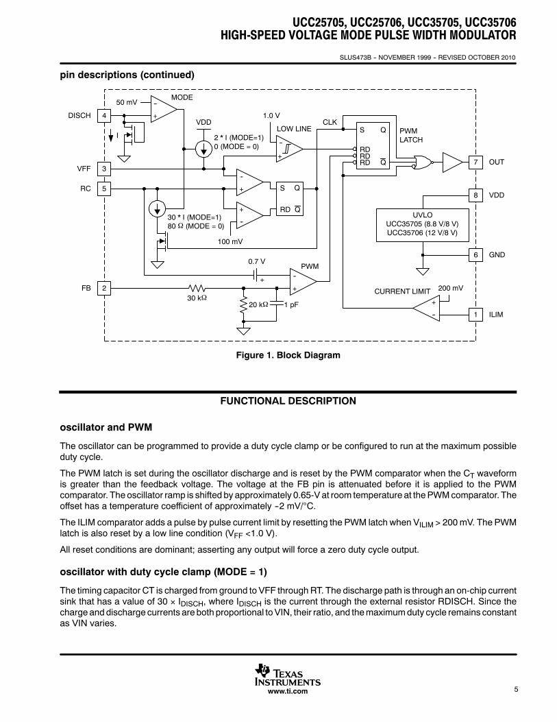
Figure 1. Block Diagram
FUNCTIONAL DESCRIPTION
oscillator and PWM
The oscillator can be programmed to provide a duty cycle clamp or be configured to run at the maximum possibleduty cycle.
The PWM latch is set during the oscillator discharge and is reset by the PWM comparator when the CT waveformis greater than the feedback voltage. The voltage at the FB pin is attenuated before it is applied to the PWMcomparator. The oscillator ramp is shifted by approximately 0.65-V at room temperature at thePWMcomparator. Theoffset has a temperature coefficient of approximately --2 mV/°C.
The ILIM comparator adds a pulse by pulse current limit by resetting the PWM latch when VILIM > 200mV. The PWMlatch is also reset by a low line condition (VFF <1.0 V).
All reset conditions are dominant; asserting any output will force a zero duty cycle output.
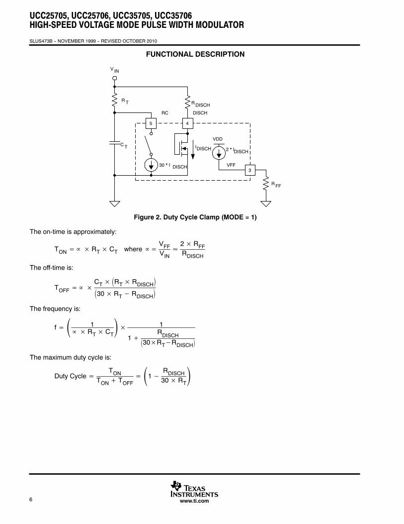
oscillator with duty cycle clamp (MODE = 1)
The timing capacitor CT is charged from ground to VFF throughRT. The discharge path is through an on-chip currentsink that has a value of 30 × IDISCH, where IDISCH is the current through the external resistor RDISCH. Since thechargeanddischarge currents are both proportional toVIN, their ratio, and themaximumduty cycle remains constantas VIN varies.
UCC25705, UCC25706, UCC35705, UCC35706HIGH-SPEED VOLTAGE MODE PULSE WIDTH MODULATOR
SLUS473B -- NOVEMBER 1999 -- REVISED OCTOBER 2010
6 www.ti.com
FUNCTIONAL DESCRIPTION
45
RC DISCH
3VFF
RFF
2 * IDISCH
RDISCHRT
CT
V IN
30 * I DISCH
VDD
IDISCH
Figure 2. Duty Cycle Clamp (MODE = 1)
The on-time is approximately:
TON=∝×RT×CT where∝=VFFVIN≈
2×RFFRDISCH
The off-time is:
TOFF=∝×CT× RT× RDISCH
30×RT−RDISCH
The frequency is:
f= 1∝× RT× CT
× 1
1+RDISCH
30×RT−RDISCH
The maximum duty cycle is:
Duty Cycle=TON
TON+ TOFF= 1− RDISCH
30×RT
UCC25705, UCC25706, UCC35705, UCC35706HIGH-SPEED VOLTAGE MODE PULSE WIDTH MODULATOR
SLUS473B -- NOVEMBER 1999 -- REVISED OCTOBER 2010
7www.ti.com
FUNCTIONAL DESCRIPTION
component selection for oscillator with duty cycle clamp (MODE = 1)
For a power converter with the following specifications:
D VIN(min) = 18 V
D VIN(max) = 75 V
D VIN(shutdown) = 15 V
D FOSC = 1 MHz
D DMAX = 0.78 at VIN(min)
In this mode, the on-time is approximately:
D TON(max) = 780 ns
D TOFF(min) = 220 ns
D VFF(min) =1815
= 1.20 V
(1) Pick CT = 220 pF.
(2) Calculate RT.
RT=VINmin × TON(max)
VFFmin ×CT
RT = 51.1 kΩ
(3) RDISCH
RDISCH=30×RT
1+⎪⎪⎪⎪
⎧
⎩
VFF(min)VIN(min)×RT×CT
TOFF(min)
⎪⎪⎪⎪
⎫
⎭RDISCH = 383 kΩ.
IDISCH must be between 25 μA and 250 μA over the entire VIN range.
With the calculated values, IDISCH ranges from 44 μA to 193 μA, within the allowable range. If IDISCH is too high, CTmust be decreased.
(4) RFF
RFF=VFF(min)× RDISCH
2× VIN(min)− 1The nearest 1% standard value to the calculated value is 13.7 k.
UCC25705, UCC25706, UCC35705, UCC35706HIGH-SPEED VOLTAGE MODE PULSE WIDTH MODULATOR
SLUS473B -- NOVEMBER 1999 -- REVISED OCTOBER 2010
8 www.ti.com
FUNCTIONAL DESCRIPTION
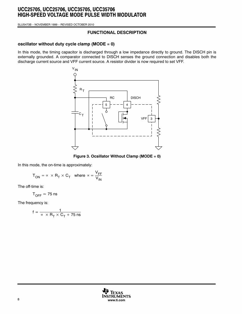
oscillator without duty cycle clamp (MODE = 0)
In this mode, the timing capacitor is discharged through a low impedance directly to ground. The DISCH pin isexternally grounded. A comparator connected to DISCH senses the ground connection and disables both thedischarge current source and VFF current source. A resistor divider is now required to set VFF.
45
RC DISCH
3VFF
RT
CT
VIN
Figure 3. Ocsillator Without Clamp (MODE = 0)
In this mode, the on-time is approximately:
TON=∝×RT×CT where∝=VFFVIN
The off-time is:
TOFF≈ 75 ns
The frequency is:
f= 1∝×RT×CT+ 75 ns
UCC25705, UCC25706, UCC35705, UCC35706HIGH-SPEED VOLTAGE MODE PULSE WIDTH MODULATOR
SLUS473B -- NOVEMBER 1999 -- REVISED OCTOBER 2010
9www.ti.com
FUNCTIONAL DESCRIPTION
component selection for oscillator without duty cycle clamp (MODE = 0)
For a power converter with the following specifications:
D VIN(min) = 18 V
D VIN(max) = 75 V
D VIN(shutdown) = 15 V
D FOSC = 1 MHz
With these specifications,
VFF(min)=1815= 1.2 V
(1) Pick CT = 220 pF
(2) Calculate RT.
RT=
VIN(min)VFF(min)
× 1FOSC
− 75 nsCT
TYPICAL CHARACTERISTICS
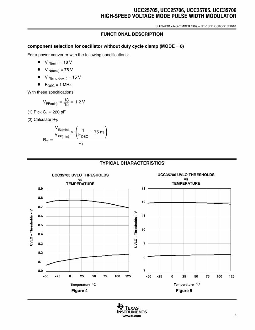
Figure 4
--50 --25 0 25 50 75 100 125
Temperature
8.0
8.1
8.2
8.3
8.4
8.5
8.6
8.7
8.8
8.9
UCC35705 UVLO THRESHOLDSvs
TEMPERATURE
°C
UVLO--Thresholds--V
Figure 5
--50 --25 0 25 50 75 100 125
Temperature
7
8
9
10
11
12
13
°C
UVLO--Thresholds--V
UCC35706 UVLO THRESHOLDSvs
TEMPERATURE
UCC25705, UCC25706, UCC35705, UCC35706HIGH-SPEED VOLTAGE MODE PULSE WIDTH MODULATOR
SLUS473B -- NOVEMBER 1999 -- REVISED OCTOBER 2010
10 www.ti.com
TYPICAL CHARACTERISTICS
Figure 6
--50 --25 0 25 50 75 100 125
Temperature
3.8
4.0
4.2
4.3
4.5
4.7
4.8
3.9
4.1
4.4
4.6
°C
I DD--mA
OPERATING CURRENT (AT 1mHz)vs
TEMPERATURE
Figure 7
--50 --25 0 25 50 75 100 125
Temperature
0.65
0.97
0.99
1.00
1.02
1.04
1.05
0.96
0.98
1.01
1.03
°C
Low-LineThreshold
--V
LOW-LINE THRESHOLDvs.
TEMPERATURE
Figure 8
--50 --25 25 50 75 100 125
Temperature
0.90
1.00
1.10
0.95
1.05
OscillatorFrequency
--MHz
OSCILLATOR FREQUENCYvs
TEMPERATURE
°C
0
Figure 9
--50 --25 0 25 50 75 100 125
Temperature
68
76
82
70
78
72
74
80
°C
ProgrammableMaximumDutyCycle--%
PROGRAMMABLE MAXIMUMDUTY CYCLE
vsTEMPERATURE
UCC25705, UCC25706, UCC35705, UCC35706HIGH-SPEED VOLTAGE MODE PULSE WIDTH MODULATOR
SLUS473B -- NOVEMBER 1999 -- REVISED OCTOBER 2010
11www.ti.com
TYPICAL CHARACTERISTICS
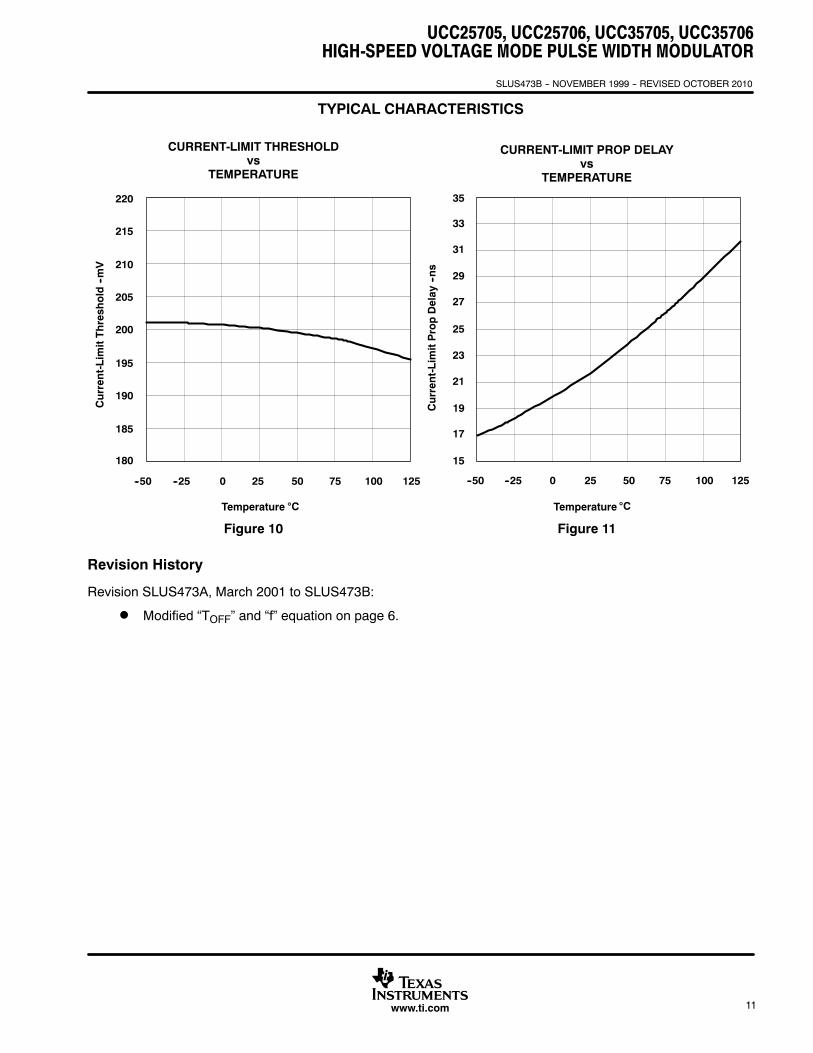
Figure 10
--50 --25 0 25 50 75 100 125
Temperature
180
200
220
185
205
190
195
210
215
°C
Current-LimitThreshold
--mV
CURRENT-LIMIT THRESHOLDvs
TEMPERATURE
Figure 11
--50 --25 0 25 50 75 100 125
Temperature
15
25
35
17
29
19
23
31
33
21
27
°C
Current-LimitPropDelay
--ns
CURRENT-LIMIT PROP DELAYvs
TEMPERATURE
Revision History
Revision SLUS473A, March 2001 to SLUS473B:
D Modified “TOFF” and “f” equation on page 6.
PACKAGE OPTION ADDENDUM
www.ti.com 10-Jun-2014
Addendum-Page 1
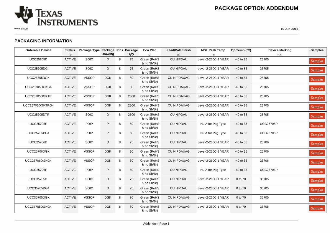
PACKAGING INFORMATION
Orderable Device Status(1)
Package Type PackageDrawing
Pins PackageQty
Eco Plan(2)
Lead/Ball Finish(6)
MSL Peak Temp(3)
Op Temp (°C) Device Marking(4/5)
Samples
UCC25705D ACTIVE SOIC D 8 75 Green (RoHS& no Sb/Br)
CU NIPDAU Level-2-260C-1 YEAR -40 to 85 25705
UCC25705DG4 ACTIVE SOIC D 8 75 Green (RoHS& no Sb/Br)
CU NIPDAU Level-2-260C-1 YEAR -40 to 85 25705
UCC25705DGK ACTIVE VSSOP DGK 8 80 Green (RoHS& no Sb/Br)
CU NIPDAUAG Level-2-260C-1 YEAR -40 to 85 25705
UCC25705DGKG4 ACTIVE VSSOP DGK 8 80 Green (RoHS& no Sb/Br)
CU NIPDAUAG Level-2-260C-1 YEAR -40 to 85 25705
UCC25705DGKTR ACTIVE VSSOP DGK 8 2500 Green (RoHS& no Sb/Br)
CU NIPDAUAG Level-2-260C-1 YEAR -40 to 85 25705
UCC25705DGKTRG4 ACTIVE VSSOP DGK 8 2500 Green (RoHS& no Sb/Br)
CU NIPDAUAG Level-2-260C-1 YEAR -40 to 85 25705
UCC25705DTR ACTIVE SOIC D 8 2500 Green (RoHS& no Sb/Br)
CU NIPDAU Level-2-260C-1 YEAR -40 to 85 25705
UCC25705P ACTIVE PDIP P 8 50 Green (RoHS& no Sb/Br)
CU NIPDAU N / A for Pkg Type -40 to 85 UCC25705P
UCC25705PG4 ACTIVE PDIP P 8 50 Green (RoHS& no Sb/Br)
CU NIPDAU N / A for Pkg Type -40 to 85 UCC25705P
UCC25706D ACTIVE SOIC D 8 75 Green (RoHS& no Sb/Br)
CU NIPDAU Level-2-260C-1 YEAR -40 to 85 25706
UCC25706DGK ACTIVE VSSOP DGK 8 80 Green (RoHS& no Sb/Br)
CU NIPDAUAG Level-2-260C-1 YEAR -40 to 85 25706
UCC25706DGKG4 ACTIVE VSSOP DGK 8 80 Green (RoHS& no Sb/Br)
CU NIPDAUAG Level-2-260C-1 YEAR -40 to 85 25706
UCC25706P ACTIVE PDIP P 8 50 Green (RoHS& no Sb/Br)
CU NIPDAU N / A for Pkg Type -40 to 85 UCC25706P
UCC35705D ACTIVE SOIC D 8 75 Green (RoHS& no Sb/Br)
CU NIPDAU Level-2-260C-1 YEAR 0 to 70 35705
UCC35705DG4 ACTIVE SOIC D 8 75 Green (RoHS& no Sb/Br)
CU NIPDAU Level-2-260C-1 YEAR 0 to 70 35705
UCC35705DGK ACTIVE VSSOP DGK 8 80 Green (RoHS& no Sb/Br)
CU NIPDAUAG Level-2-260C-1 YEAR 0 to 70 35705
UCC35705DGKG4 ACTIVE VSSOP DGK 8 80 Green (RoHS& no Sb/Br)
CU NIPDAUAG Level-2-260C-1 YEAR 0 to 70 35705
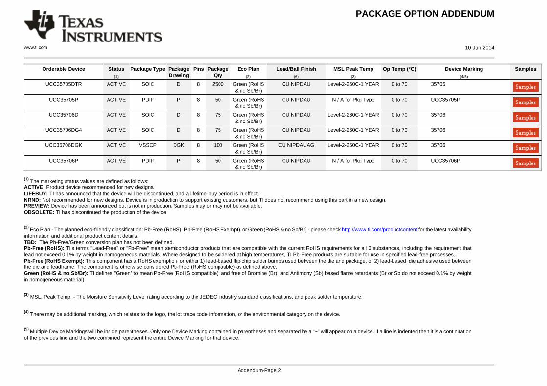
PACKAGE OPTION ADDENDUM
www.ti.com 10-Jun-2014
Addendum-Page 2
Orderable Device Status(1)
Package Type PackageDrawing
Pins PackageQty
Eco Plan(2)
Lead/Ball Finish(6)
MSL Peak Temp(3)
Op Temp (°C) Device Marking(4/5)
Samples
UCC35705DTR ACTIVE SOIC D 8 2500 Green (RoHS& no Sb/Br)
CU NIPDAU Level-2-260C-1 YEAR 0 to 70 35705
UCC35705P ACTIVE PDIP P 8 50 Green (RoHS& no Sb/Br)
CU NIPDAU N / A for Pkg Type 0 to 70 UCC35705P
UCC35706D ACTIVE SOIC D 8 75 Green (RoHS& no Sb/Br)
CU NIPDAU Level-2-260C-1 YEAR 0 to 70 35706
UCC35706DG4 ACTIVE SOIC D 8 75 Green (RoHS& no Sb/Br)
CU NIPDAU Level-2-260C-1 YEAR 0 to 70 35706
UCC35706DGK ACTIVE VSSOP DGK 8 100 Green (RoHS& no Sb/Br)
CU NIPDAUAG Level-2-260C-1 YEAR 0 to 70 35706
UCC35706P ACTIVE PDIP P 8 50 Green (RoHS& no Sb/Br)
CU NIPDAU N / A for Pkg Type 0 to 70 UCC35706P
(1) The marketing status values are defined as follows:ACTIVE: Product device recommended for new designs.LIFEBUY: TI has announced that the device will be discontinued, and a lifetime-buy period is in effect.NRND: Not recommended for new designs. Device is in production to support existing customers, but TI does not recommend using this part in a new design.PREVIEW: Device has been announced but is not in production. Samples may or may not be available.OBSOLETE: TI has discontinued the production of the device.
(2) Eco Plan - The planned eco-friendly classification: Pb-Free (RoHS), Pb-Free (RoHS Exempt), or Green (RoHS & no Sb/Br) - please check http://www.ti.com/productcontent for the latest availabilityinformation and additional product content details.TBD: The Pb-Free/Green conversion plan has not been defined.Pb-Free (RoHS): TI's terms "Lead-Free" or "Pb-Free" mean semiconductor products that are compatible with the current RoHS requirements for all 6 substances, including the requirement thatlead not exceed 0.1% by weight in homogeneous materials. Where designed to be soldered at high temperatures, TI Pb-Free products are suitable for use in specified lead-free processes.Pb-Free (RoHS Exempt): This component has a RoHS exemption for either 1) lead-based flip-chip solder bumps used between the die and package, or 2) lead-based die adhesive used betweenthe die and leadframe. The component is otherwise considered Pb-Free (RoHS compatible) as defined above.Green (RoHS & no Sb/Br): TI defines "Green" to mean Pb-Free (RoHS compatible), and free of Bromine (Br) and Antimony (Sb) based flame retardants (Br or Sb do not exceed 0.1% by weightin homogeneous material)
(3) MSL, Peak Temp. - The Moisture Sensitivity Level rating according to the JEDEC industry standard classifications, and peak solder temperature.
(4) There may be additional marking, which relates to the logo, the lot trace code information, or the environmental category on the device.
(5) Multiple Device Markings will be inside parentheses. Only one Device Marking contained in parentheses and separated by a "~" will appear on a device. If a line is indented then it is a continuationof the previous line and the two combined represent the entire Device Marking for that device.
PACKAGE OPTION ADDENDUM
www.ti.com 10-Jun-2014
Addendum-Page 3
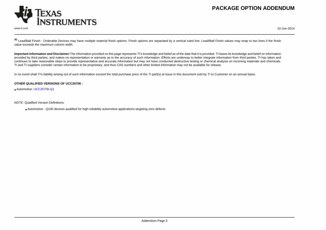
(6) Lead/Ball Finish - Orderable Devices may have multiple material finish options. Finish options are separated by a vertical ruled line. Lead/Ball Finish values may wrap to two lines if the finishvalue exceeds the maximum column width.
Important Information and Disclaimer:The information provided on this page represents TI's knowledge and belief as of the date that it is provided. TI bases its knowledge and belief on informationprovided by third parties, and makes no representation or warranty as to the accuracy of such information. Efforts are underway to better integrate information from third parties. TI has taken andcontinues to take reasonable steps to provide representative and accurate information but may not have conducted destructive testing or chemical analysis on incoming materials and chemicals.TI and TI suppliers consider certain information to be proprietary, and thus CAS numbers and other limited information may not be available for release.
In no event shall TI's liability arising out of such information exceed the total purchase price of the TI part(s) at issue in this document sold by TI to Customer on an annual basis.
OTHER QUALIFIED VERSIONS OF UCC25706 :
• Automotive: UCC25706-Q1
NOTE: Qualified Version Definitions:
• Automotive - Q100 devices qualified for high-reliability automotive applications targeting zero defects
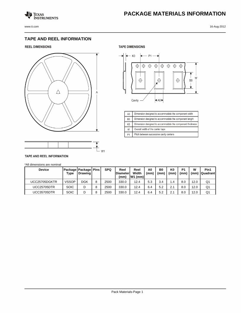
TAPE AND REEL INFORMATION
*All dimensions are nominal
Device PackageType
PackageDrawing
Pins SPQ ReelDiameter
(mm)
ReelWidth
W1 (mm)
A0(mm)
B0(mm)
K0(mm)
P1(mm)
W(mm)
Pin1Quadrant
UCC25705DGKTR VSSOP DGK 8 2500 330.0 12.4 5.3 3.4 1.4 8.0 12.0 Q1
UCC25705DTR SOIC D 8 2500 330.0 12.4 6.4 5.2 2.1 8.0 12.0 Q1
UCC35705DTR SOIC D 8 2500 330.0 12.4 6.4 5.2 2.1 8.0 12.0 Q1
PACKAGE MATERIALS INFORMATION
www.ti.com 16-Aug-2012
Pack Materials-Page 1
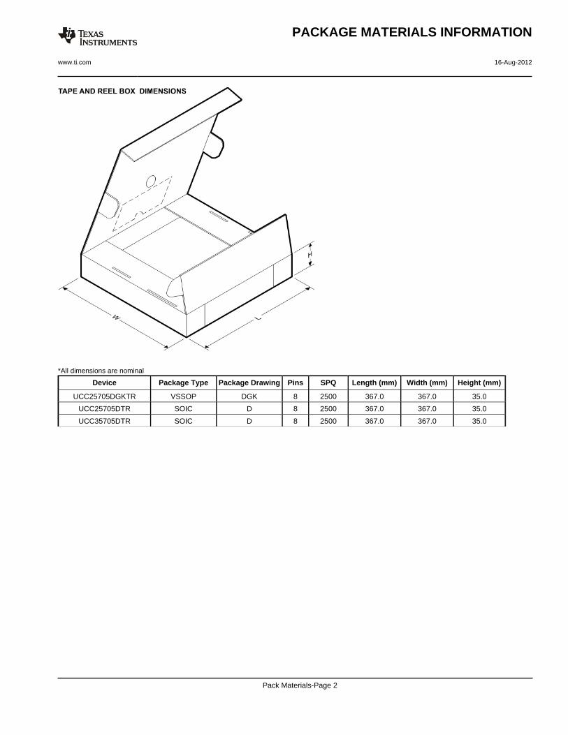
*All dimensions are nominal
Device Package Type Package Drawing Pins SPQ Length (mm) Width (mm) Height (mm)
UCC25705DGKTR VSSOP DGK 8 2500 367.0 367.0 35.0
UCC25705DTR SOIC D 8 2500 367.0 367.0 35.0
UCC35705DTR SOIC D 8 2500 367.0 367.0 35.0
PACKAGE MATERIALS INFORMATION
www.ti.com 16-Aug-2012
Pack Materials-Page 2

IMPORTANT NOTICE
Texas Instruments Incorporated and its subsidiaries (TI) reserve the right to make corrections, enhancements, improvements and otherchanges to its semiconductor products and services per JESD46, latest issue, and to discontinue any product or service per JESD48, latestissue. Buyers should obtain the latest relevant information before placing orders and should verify that such information is current andcomplete. All semiconductor products (also referred to herein as “components”) are sold subject to TI’s terms and conditions of salesupplied at the time of order acknowledgment.TI warrants performance of its components to the specifications applicable at the time of sale, in accordance with the warranty in TI’s termsand conditions of sale of semiconductor products. Testing and other quality control techniques are used to the extent TI deems necessaryto support this warranty. Except where mandated by applicable law, testing of all parameters of each component is not necessarilyperformed.TI assumes no liability for applications assistance or the design of Buyers’ products. Buyers are responsible for their products andapplications using TI components. To minimize the risks associated with Buyers’ products and applications, Buyers should provideadequate design and operating safeguards.TI does not warrant or represent that any license, either express or implied, is granted under any patent right, copyright, mask work right, orother intellectual property right relating to any combination, machine, or process in which TI components or services are used. Informationpublished by TI regarding third-party products or services does not constitute a license to use such products or services or a warranty orendorsement thereof. Use of such information may require a license from a third party under the patents or other intellectual property of thethird party, or a license from TI under the patents or other intellectual property of TI.Reproduction of significant portions of TI information in TI data books or data sheets is permissible only if reproduction is without alterationand is accompanied by all associated warranties, conditions, limitations, and notices. TI is not responsible or liable for such altereddocumentation. Information of third parties may be subject to additional restrictions.Resale of TI components or services with statements different from or beyond the parameters stated by TI for that component or servicevoids all express and any implied warranties for the associated TI component or service and is an unfair and deceptive business practice.TI is not responsible or liable for any such statements.Buyer acknowledges and agrees that it is solely responsible for compliance with all legal, regulatory and safety-related requirementsconcerning its products, and any use of TI components in its applications, notwithstanding any applications-related information or supportthat may be provided by TI. Buyer represents and agrees that it has all the necessary expertise to create and implement safeguards whichanticipate dangerous consequences of failures, monitor failures and their consequences, lessen the likelihood of failures that might causeharm and take appropriate remedial actions. Buyer will fully indemnify TI and its representatives against any damages arising out of the useof any TI components in safety-critical applications.In some cases, TI components may be promoted specifically to facilitate safety-related applications. With such components, TI’s goal is tohelp enable customers to design and create their own end-product solutions that meet applicable functional safety standards andrequirements. Nonetheless, such components are subject to these terms.No TI components are authorized for use in FDA Class III (or similar life-critical medical equipment) unless authorized officers of the partieshave executed a special agreement specifically governing such use.Only those TI components which TI has specifically designated as military grade or “enhanced plastic” are designed and intended for use inmilitary/aerospace applications or environments. Buyer acknowledges and agrees that any military or aerospace use of TI componentswhich have not been so designated is solely at the Buyer's risk, and that Buyer is solely responsible for compliance with all legal andregulatory requirements in connection with such use.TI has specifically designated certain components as meeting ISO/TS16949 requirements, mainly for automotive use. In any case of use ofnon-designated products, TI will not be responsible for any failure to meet ISO/TS16949.
Products ApplicationsAudio www.ti.com/audio Automotive and Transportation www.ti.com/automotiveAmplifiers amplifier.ti.com Communications and Telecom www.ti.com/communicationsData Converters dataconverter.ti.com Computers and Peripherals www.ti.com/computersDLP® Products www.dlp.com Consumer Electronics www.ti.com/consumer-appsDSP dsp.ti.com Energy and Lighting www.ti.com/energyClocks and Timers www.ti.com/clocks Industrial www.ti.com/industrialInterface interface.ti.com Medical www.ti.com/medicalLogic logic.ti.com Security www.ti.com/securityPower Mgmt power.ti.com Space, Avionics and Defense www.ti.com/space-avionics-defenseMicrocontrollers microcontroller.ti.com Video and Imaging www.ti.com/videoRFID www.ti-rfid.comOMAP Applications Processors www.ti.com/omap TI E2E Community e2e.ti.comWireless Connectivity www.ti.com/wirelessconnectivity
Mailing Address: Texas Instruments, Post Office Box 655303, Dallas, Texas 75265Copyright © 2016, Texas Instruments Incorporated