6.976 High Speed Communication Circuits and Systems Lecture 20
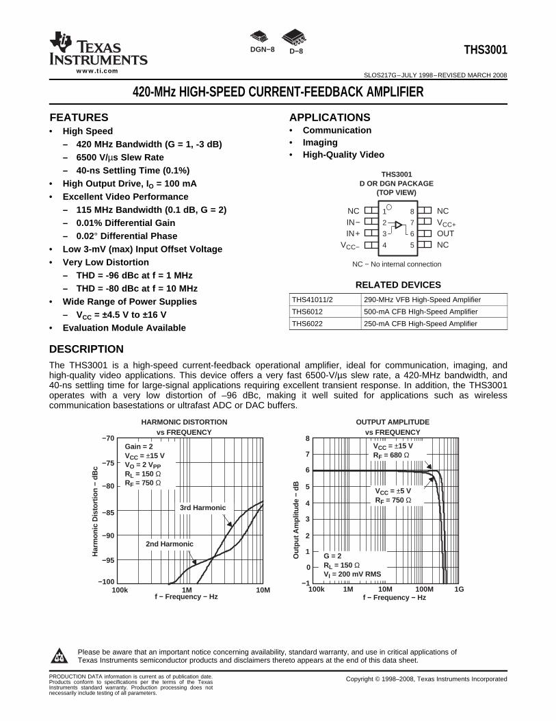
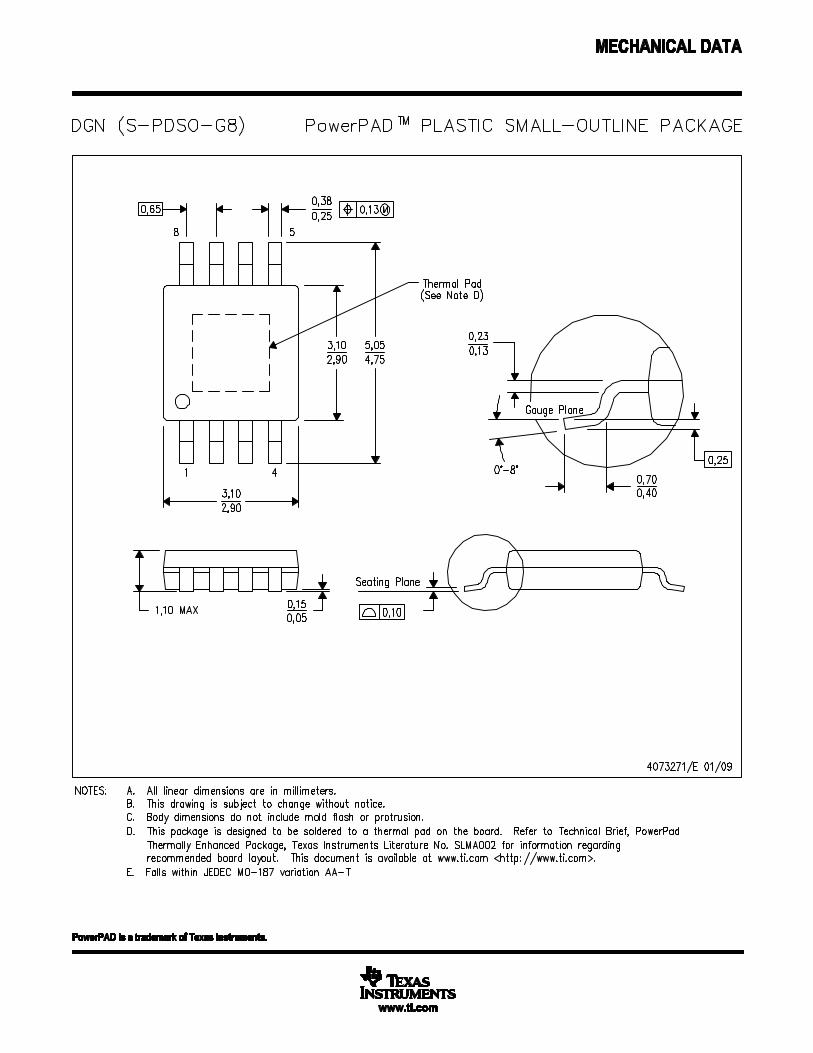
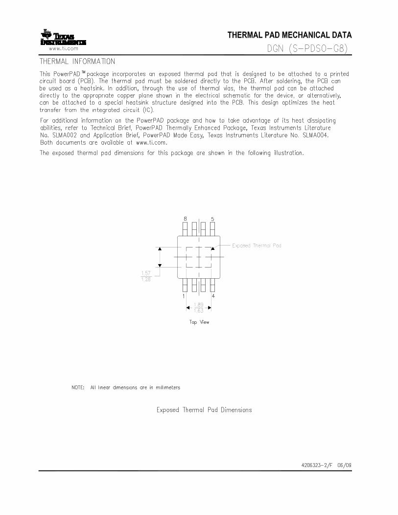
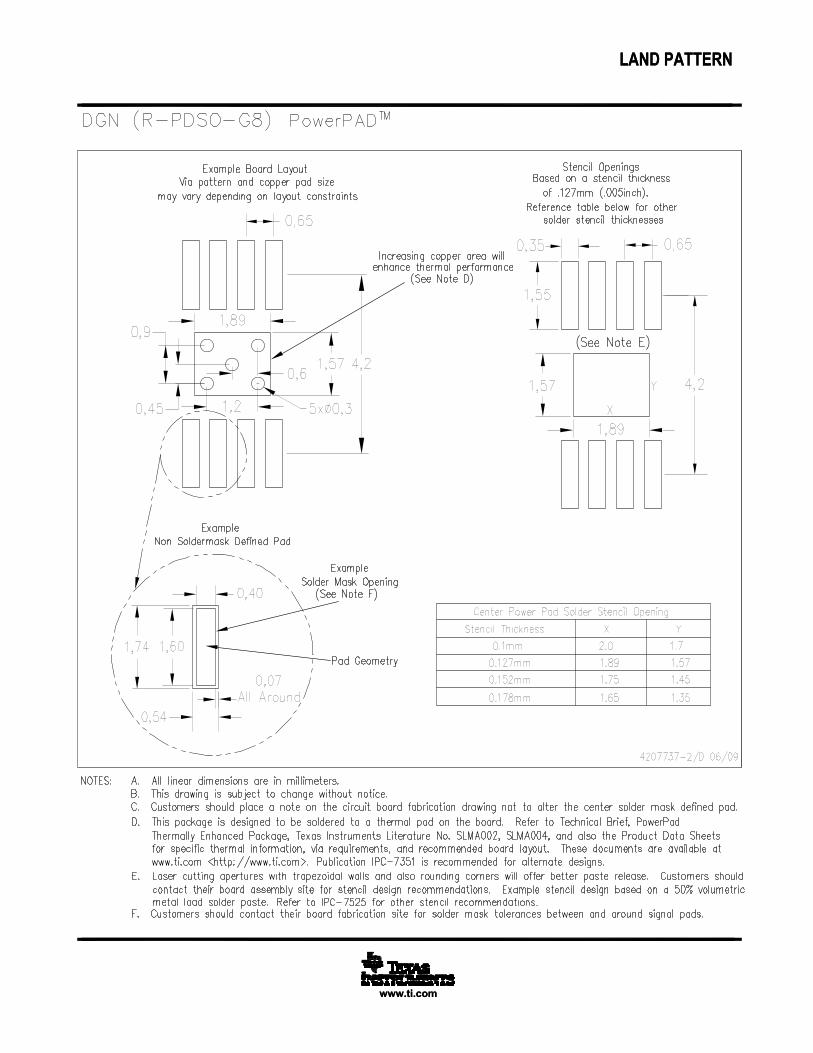
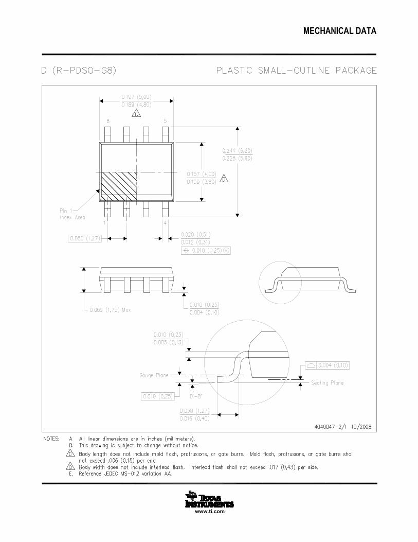
DGN−8 D−8
1FEATURES APPLICATIONS
NC − No internal connection
1
2
3
4
8
7
6
5
NCIN−IN+
VCC−
NCVCC+OUTNC
THS3001D OR DGN PACKAGE
(TOP VIEW)
DESCRIPTION
f − Frequency − Hz
OUTPUT AMPLITUDEvs FREQUENCY
5
3
1
−11M 100M
6
4
2
0
10M 1G100k
7
8
Out
put
Am
plitu
de −
dB
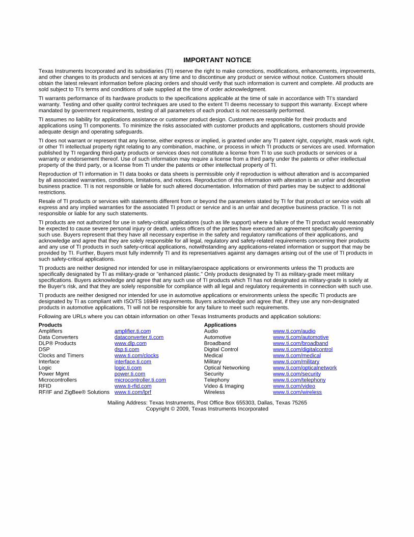
G = 2RL = 150 ΩVI = 200 mV RMS
HARMONIC DISTORTIONvs FREQUENCY
−70
−80
−90
−100
−75
−85
−95
Har
mon
ic D
isto
rtion
− d
Bc
Gain = 2VCC = ±15 VVO = 2 VPPRL = 150 ΩRF = 750 Ω
100k 1M 10Mf − Frequency − Hz
VCC = ±15 VRF = 680 Ω
VCC = ±5 VRF = 750 Ω
3rd Harmonic
2nd Harmonic
THS3001
SLOS217G–JULY 1998–REVISED MARCH 2008www.ti.com
420-MHz HIGH-SPEED CURRENT-FEEDBACK AMPLIFIER
• Communication• High Speed• Imaging– 420 MHz Bandwidth (G = 1, -3 dB)• High-Quality Video– 6500 V/µs Slew Rate
– 40-ns Settling Time (0.1%)• High Output Drive, IO = 100 mA• Excellent Video Performance
– 115 MHz Bandwidth (0.1 dB, G = 2)– 0.01% Differential Gain– 0.02° Differential Phase
• Low 3-mV (max) Input Offset Voltage• Very Low Distortion
– THD = -96 dBc at f = 1 MHzRELATED DEVICES– THD = -80 dBc at f = 10 MHz
THS41011/2 290-MHz VFB High-Speed Amplifier• Wide Range of Power SuppliesTHS6012 500-mA CFB HIgh-Speed Amplifier– VCC = ±4.5 V to ±16 VTHS6022 250-mA CFB High-Speed Amplifier• Evaluation Module Available
The THS3001 is a high-speed current-feedback operational amplifier, ideal for communication, imaging, andhigh-quality video applications. This device offers a very fast 6500-V/µs slew rate, a 420-MHz bandwidth, and40-ns settling time for large-signal applications requiring excellent transient response. In addition, the THS3001operates with a very low distortion of –96 dBc, making it well suited for applications such as wirelesscommunication basestations or ultrafast ADC or DAC buffers.
1
Please be aware that an important notice concerning availability, standard warranty, and use in critical applications ofTexas Instruments semiconductor products and disclaimers thereto appears at the end of this data sheet.
PRODUCTION DATA information is current as of publication date. Copyright © 1998–2008, Texas Instruments IncorporatedProducts conform to specifications per the terms of the TexasInstruments standard warranty. Production processing does notnecessarily include testing of all parameters.
www.ti.com
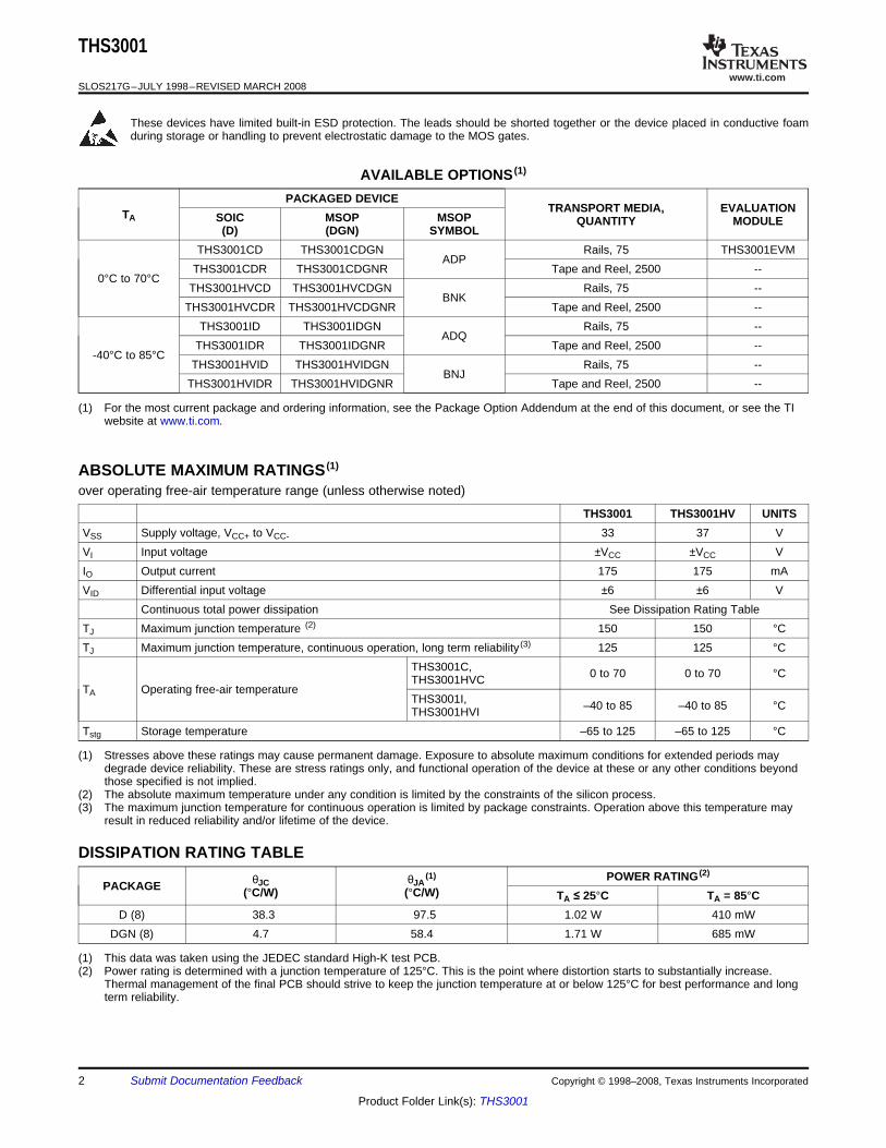
ABSOLUTE MAXIMUM RATINGS (1)
DISSIPATION RATING TABLE
THS3001
SLOS217G–JULY 1998–REVISED MARCH 2008
These devices have limited built-in ESD protection. The leads should be shorted together or the device placed in conductive foamduring storage or handling to prevent electrostatic damage to the MOS gates.
AVAILABLE OPTIONS (1)
PACKAGED DEVICETRANSPORT MEDIA, EVALUATIONTA SOIC MSOP MSOP QUANTITY MODULE
(D) (DGN) SYMBOLTHS3001CD THS3001CDGN Rails, 75 THS3001EVM
ADPTHS3001CDR THS3001CDGNR Tape and Reel, 2500 --
0°C to 70°CTHS3001HVCD THS3001HVCDGN Rails, 75 --
BNKTHS3001HVCDR THS3001HVCDGNR Tape and Reel, 2500 --
THS3001ID THS3001IDGN Rails, 75 --ADQ
THS3001IDR THS3001IDGNR Tape and Reel, 2500 ---40°C to 85°C
THS3001HVID THS3001HVIDGN Rails, 75 --BNJ
THS3001HVIDR THS3001HVIDGNR Tape and Reel, 2500 --
(1) For the most current package and ordering information, see the Package Option Addendum at the end of this document, or see the TIwebsite at www.ti.com.
over operating free-air temperature range (unless otherwise noted)
THS3001 THS3001HV UNITSVSS Supply voltage, VCC+ to VCC- 33 37 VVI Input voltage ±VCC ±VCC VIO Output current 175 175 mAVID Differential input voltage ±6 ±6 V
Continuous total power dissipation See Dissipation Rating TableTJ Maximum junction temperature (2) 150 150 °CTJ Maximum junction temperature, continuous operation, long term reliability (3) 125 125 °C
THS3001C, 0 to 70 0 to 70 °CTHS3001HVCTA Operating free-air temperature
THS3001I, –40 to 85 –40 to 85 °CTHS3001HVITstg Storage temperature –65 to 125 –65 to 125 °C
(1) Stresses above these ratings may cause permanent damage. Exposure to absolute maximum conditions for extended periods maydegrade device reliability. These are stress ratings only, and functional operation of the device at these or any other conditions beyondthose specified is not implied.
(2) The absolute maximum temperature under any condition is limited by the constraints of the silicon process.(3) The maximum junction temperature for continuous operation is limited by package constraints. Operation above this temperature may
result in reduced reliability and/or lifetime of the device.
POWER RATING (2)θJC θJA
(1)PACKAGE (°C/W) (°C/W) TA ≤ 25°C TA = 85°C
D (8) 38.3 97.5 1.02 W 410 mWDGN (8) 4.7 58.4 1.71 W 685 mW
(1) This data was taken using the JEDEC standard High-K test PCB.(2) Power rating is determined with a junction temperature of 125°C. This is the point where distortion starts to substantially increase.
Thermal management of the final PCB should strive to keep the junction temperature at or below 125°C for best performance and longterm reliability.
2 Submit Documentation Feedback Copyright © 1998–2008, Texas Instruments Incorporated
Product Folder Link(s): THS3001
www.ti.com
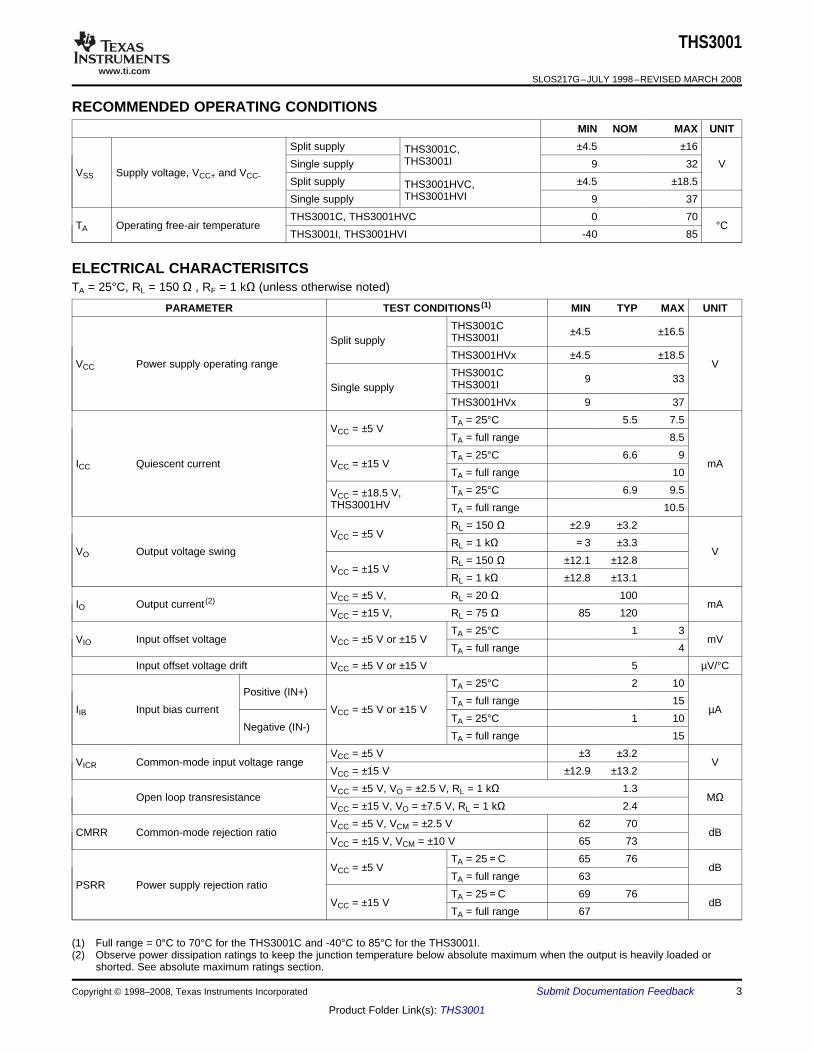
RECOMMENDED OPERATING CONDITIONS
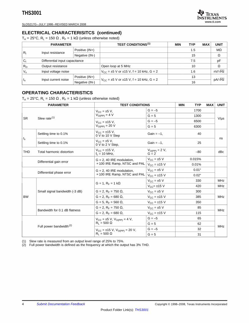
ELECTRICAL CHARACTERISITCS
THS3001
SLOS217G–JULY 1998–REVISED MARCH 2008
MIN NOM MAX UNITSplit supply ±4.5 ±16THS3001C,
THS3001ISingle supply 9 32 VVSS Supply voltage, VCC+ and VCC- Split supply ±4.5 ±18.5THS3001HVC,
THS3001HVISingle supply 9 37THS3001C, THS3001HVC 0 70
TA Operating free-air temperature °CTHS3001I, THS3001HVI -40 85
TA = 25°C, RL = 150 Ω , RF = 1 kΩ (unless otherwise noted)
PARAMETER TEST CONDITIONS (1) MIN TYP MAX UNITTHS3001C ±4.5 ±16.5THS3001ISplit supplyTHS3001HVx ±4.5 ±18.5
VCC Power supply operating range VTHS3001C 9 33THS3001ISingle supplyTHS3001HVx 9 37TA = 25°C 5.5 7.5
VCC = ±5 VTA = full range 8.5TA = 25°C 6.6 9
ICC Quiescent current VCC = ±15 V mATA = full range 10TA = 25°C 6.9 9.5VCC = ±18.5 V,
THS3001HV TA = full range 10.5RL = 150 Ω ±2.9 ±3.2
VCC = ±5 VRL = 1 kΩ =3 ±3.3
VO Output voltage swing VRL = 150 Ω ±12.1 ±12.8
VCC = ±15 VRL = 1 kΩ ±12.8 ±13.1
VCC = ±5 V, RL = 20 Ω 100IO Output current (2) mA
VCC = ±15 V, RL = 75 Ω 85 120TA = 25°C 1 3
VIO Input offset voltage VCC = ±5 V or ±15 V mVTA = full range 4
Input offset voltage drift VCC = ±5 V or ±15 V 5 µV/°CTA = 25°C 2 10
Positive (IN+)TA = full range 15
IIB Input bias current VCC = ±5 V or ±15 V µATA = 25°C 1 10
Negative (IN-)TA = full range 15
VCC = ±5 V ±3 ±3.2VICR Common-mode input voltage range V
VCC = ±15 V ±12.9 ±13.2VCC = ±5 V, VO = ±2.5 V, RL = 1 kΩ 1.3
Open loop transresistance MΩVCC = ±15 V, VO = ±7.5 V, RL = 1 kΩ 2.4VCC = ±5 V, VCM = ±2.5 V 62 70
CMRR Common-mode rejection ratio dBVCC = ±15 V, VCM = ±10 V 65 73
TA = 25=C 65 76VCC = ±5 V dB
TA = full range 63PSRR Power supply rejection ratio
TA = 25=C 69 76VCC = ±15 V dB
TA = full range 67
(1) Full range = 0°C to 70°C for the THS3001C and -40°C to 85°C for the THS3001I.(2) Observe power dissipation ratings to keep the junction temperature below absolute maximum when the output is heavily loaded or
shorted. See absolute maximum ratings section.
Copyright © 1998–2008, Texas Instruments Incorporated Submit Documentation Feedback 3
Product Folder Link(s): THS3001
www.ti.com
OPERATING CHARACTERISTICS
THS3001
SLOS217G–JULY 1998–REVISED MARCH 2008
ELECTRICAL CHARACTERISITCS (continued)TA = 25°C, RL = 150 Ω , RF = 1 kΩ (unless otherwise noted)
PARAMETER TEST CONDITIONS (1) MIN TYP MAX UNITPositive (IN+) 1.5 MΩ
RI Input resistanceNegative (IN-) 15 Ω
CI Differential input capacitance 7.5 pFRO Output resistance Open loop at 5 MHz 10 ΩVn Input voltage noise VCC = ±5 V or ±15 V, f = 10 kHz, G = 2 1.6 nV/√Hz
Positive (IN+) 13In Input current noise VCC = ±5 V or ±15 V, f = 10 kHz, G = 2 pA/√Hz
Negative (IN-) 16
TA = 25°C, RL = 150 Ω , RF = 1 kΩ (unless otherwise noted)
PARAMETER TEST CONDITIONS MIN TYP MAX UNITG = –5 1700VCC = ±5 V,
VO(PP) = 4 V G = 5 1300SR Slew rate (1) V/µs
G = –5 6500VCC = ±15 V,VO(PP) = 20 V G = 5 6300VCC = ±15 V,Settling time to 0.1% Gain = –1, 400 V to 10 V Step
ts nsVCC = ±5 V,Settling time to 0.1% Gain = –1, 250 V to 2 V Step,VCC = ±15 V, VO(PP) = 2 V,THD Total harmonic distortion –80 dBcfc = 10 MHz, G = 2
VCC = ±5 V 0.015%G = 2, 40 IRE modulation,Differential gain error =100 IRE Ramp, NTSC and PAL VCC = ±15 V 0.01%VCC = ±5 V 0.01°G = 2, 40 IRE modulation,Differential phase error =100 IRE Ramp, NTSC and PAL VCC = ±15 V 0.02°
VCC = ±5 V 330 MHzG = 1, RF = 1 kΩ
VCC= ±15 V 420 MHzSmall signal bandwidth (-3 dB) G = 2, RF = 750 Ω, VCC = ±5 V 300
BW G = 2, RF = 680 Ω, VCC = ±15 V 385 MHzG = 5, RF = 560 Ω, VCC = ±15 V 350G = 2, RF = 750 Ω, VCC = ±5 V 85
Bandwidth for 0.1 dB flatness MHzG = 2, RF = 680 Ω, VCC = ±15 V 115
G = –5 65VCC = ±5 V, VO(PP) = 4 V,RL = 500 Ω G = 5 62
Full power bandwidth (2) MHzG = –5 32VCC = ±15 V, VO(PP) = 20 V,
RL = 500 Ω G = 5 31
(1) Slew rate is measured from an output level range of 25% to 75%.(2) Full power bandwidth is defined as the frequency at which the output has 3% THD.
4 Submit Documentation Feedback Copyright © 1998–2008, Texas Instruments Incorporated
Product Folder Link(s): THS3001
www.ti.com
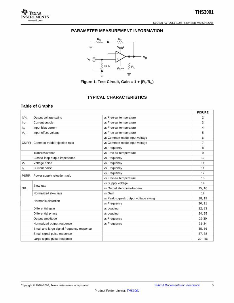
PARAMETER MEASUREMENT INFORMATION
VIVO+
−
RG RF
RL50 ΩVCC−
VCC+
TYPICAL CHARACTERISTICS
Table of Graphs
THS3001
SLOS217G–JULY 1998–REVISED MARCH 2008
Figure 1. Test Circuit, Gain = 1 + (RF/RG)
FIGURE|VO| Output voltage swing vs Free-air temperature 2ICC Current supply vs Free-air temperature 3IIB Input bias current vs Free-air temperature 4VIO Input offset voltage vs Free-air temperature 5
vs Common-mode input voltage 6CMRR Common-mode rejection ratio vs Common-mode input voltage 7
vs Frequency 8Transresistance vs Free-air temperature 9Closed-loop output impedance vs Frequency 10
Vn Voltage noise vs Frequency 11In Current noise vs Frequency 11
vs Frequency 12PSRR Power supply rejection ratio
vs Free-air temperature 13vs Supply voltage 14
Slew rateSR vs Output step peak-to-peak 15, 16
Normalized slew rate vs Gain 17vs Peak-to-peak output voltage swing 18, 19
Harmonic distortionvs Frequency 20, 21
Differential gain vs Loading 22, 23Differential phase vs Loading 24, 25Output amplitude vs Frequency 26-30Normalized output response vs Frequency 31-34Small and large signal frequency response 35, 36Small signal pulse response 37, 38Large signal pulse response 39 - 46
Copyright © 1998–2008, Texas Instruments Incorporated Submit Documentation Feedback 5
Product Folder Link(s): THS3001
www.ti.com
TA − Free-Air T emperature − °C
12
2−20 20
14
4
0 40 100−40 60 80
O −
Out
put V
olta
ge S
win
g −
VV
12.5
13
13.5
3.5
3
2.5
VCC = ±5 VRL = 150 Ω
VCC = ±5 VNo Load
VCC = ±15 VRL = 150 Ω
VCC = ±15 VNo Load
TA − Free-Air T emperature − °C
9
7
5
3−20 20
8
6
4
0 40 100−40 60 80
VCC = ±5 V
VCC = ±15 V
VCC = ±10 V
I CC
− S
uppl
y C
urre
nt −
mA
TA − Free-Air T emperature − °C
0
−0.4
−0.8
−1.2−20 20
−0.2
−0.6
−1
0 40 100−40 60 80
VCC = ±5 V
VCC = ±15 V
Gain = 1RF = 1 kΩ
VIO
− In
put O
ffset
Vol
tage
− m
V
−40 −20 0 20 80 100
TA − Free-Air T emperature − °C6040
I IB
− In
put B
ias
Cur
rent
−
−1
−2
−3
−0.5
−1.5
−2.5
Aµ
VCC = ±5 V
VCC = ±15 V
VCC = ±5 V
VCC = ±15 V
IIB−
IIB−
IIB+
IIB+
THS3001
SLOS217G–JULY 1998–REVISED MARCH 2008
OUTPUT VOLTAGE SWING CURRENT SUPPLYvs vs
FREE-AIR TEMPERATURE FREE-AIR TEMPERATURE
Figure 2. Figure 3.
INPUT BIAS CURRENT INPUT OFFSET VOLTAGEvs vs
FREE-AIR TEMPERATURE FREE-AIR TEMPERATURE
Figure 4. Figure 5.
6 Submit Documentation Feedback Copyright © 1998–2008, Texas Instruments Incorporated
Product Folder Link(s): THS3001
www.ti.com
|VIC| − Common-Mode Input V oltage − V
60
50
40
302 64 8 14
80
0 10 12
70
TA = −40°C
CM
RR
− C
omm
on-M
ode
Rej
ectio
n R
atio
− d
B
TA = 85°CTA = 25°C
VCC = ±15 V
|VIC| − Common-Mode Input V oltage − V
50
40
30
200.5 1.51 2 4
80
0 2.5 3
60
TA = −40°C
CM
RR
− C
omm
on-M
ode
Rej
ectio
n R
atio
− d
B
TA = 85°C
TA = 25°C
VCC = ±5 V
3.5
70
f − Frequency − Hz
1k 10k 10M 100M1M100k
60
40
20
0
50
30
10
80
70
VCC = ±5 V
VCC = ±15 V
CM
RR
− C
omm
on-M
ode
Rej
ectio
n R
atio
− d
B
1 kΩ
1 kΩ
VI +− VO
1 kΩ1 kΩ
TA − Free-Air T emperature − °C
2.2
1.8
1.4
1−20 20
2.4
2
1.6
1.2
0 40 100
VO = VCC/2RL = 1 kΩ
2.8
−40 60 80
2.6
Tran
sres
ista
nce
− M
Ω
VCC = ±5 V
VCC = ±15 V
VCC = ±10 V
THS3001
SLOS217G–JULY 1998–REVISED MARCH 2008
COMMON-MODE REJECTION RATIO COMMON-MODE REJECTION RATIOvs vs
COMMON-MODE INPUT VOLTAGE COMMON-MODE INPUT VOLTAGE
Figure 6. Figure 7.
COMMON-MODE REJECTION RATIO TRANSRESISTANCEvs vs
FREQUENCY FREE-AIR TEMPERATURE
Figure 8. Figure 9.
Copyright © 1998–2008, Texas Instruments Incorporated Submit Documentation Feedback 7
Product Folder Link(s): THS3001
www.ti.com
10
1
0.1
0.011M
f − Frequency − Hz100k 10M 100M
100
Clo
sed-
Loop
Out
put I
mpe
danc
e −
VCC = ±15 VRF = 750 ΩGain = +2TA = 25°CVI(PP) = 2 V
1G
Ω
VO
+
−
50 Ω
750 Ω1 kΩ
VI
THS3001
750 Ω
( VO
VI=
1000
Zo ) − 1
f − Frequency − Hz
100
10
1100 10k1k 100k10
1000VCC = ±15 V and ±5 VTA = 25°C
In−
nV/
Hz
− Vo
ltage
Noi
se −
Vn I n
− C
urre
nt N
oise
−pA
/H
zand
In+
Vn
TA − Free-Air T emperature − °C
80
70−20 20
85
75
0 40 100−40 60 80
90
PS
RR
− P
ower
Sup
ply
Rej
ectio
n R
atio
− d
B
VCC = +5 V
VCC = +15 V
VCC = −5 V
VCC = −15 V
f − Frequency − Hz
PS
RR
− P
ower
Sup
ply
Rej
ectio
n R
atio
− d
B
1k 10k 10M 100M1M100k
60
40
20
0
50
30
10
80
90
70
VCC = ±5 V
VCC = ±15 V
G = 1RF = 1 kΩ
VCC = ±5 V
VCC = ±15 V
−PSRR
+PSRR
THS3001
SLOS217G–JULY 1998–REVISED MARCH 2008
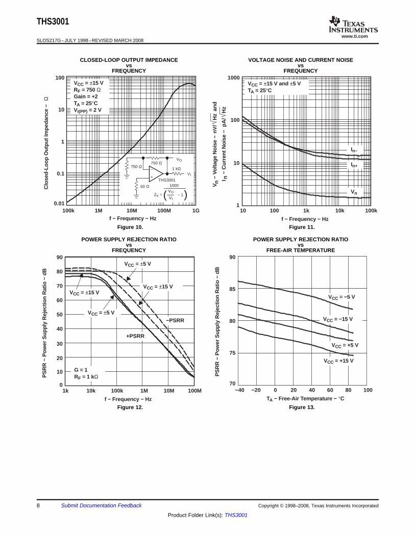
CLOSED-LOOP OUTPUT IMPEDANCE VOLTAGE NOISE AND CURRENT NOISEvs vs
FREQUENCY FREQUENCY
Figure 10. Figure 11.
POWER SUPPLY REJECTION RATIO POWER SUPPLY REJECTION RATIOvs vs
FREQUENCY FREE-AIR TEMPERATURE
Figure 12. Figure 13.
8 Submit Documentation Feedback Copyright © 1998–2008, Texas Instruments Incorporated
Product Folder Link(s): THS3001
www.ti.com
VO(PP) − Output Step − V
10000
1005 15
1000
10 200
VCC = ±15 VG = +5RL = 150 Ωtr/tf = 300 psRF = 1 kΩ
SR
− S
lew
Rat
e −
V/µ
s
+SR
−SR
|VCC| − Supply V oltage − V
4000
3000
2000
10007 119 13
6000
5 15
5000
G = +5RL = 150 Ωtr/tf = 300 psRF = 1 kΩ
SR
− S
lew
Rat
e −
V/µ
s
−SR
+SR
7000
G − Gain − V/V
1.3
1.1
0.9
0.72 4
1.2
1
0.8
3 5 101 6 7
−Gain
+Gain
8 9
1.5
1.4
VCC = ±5 VVO(PP) = 4 VRL = 150 ΩRF = 1 kΩtr/tf = 300 ps
SR
− N
orm
aliz
ed S
lew
Rat
e −
V/
µs
VO(PP) − Output Step − V
2000
1001 3
1000
2 40 5
VCC = ±5 VG = +5RL = 150 Ωtr/tf = 300 psRF= 1 kΩ
−SR
+SR
SR
− S
lew
Rat
e −
V/µ
s
THS3001
SLOS217G–JULY 1998–REVISED MARCH 2008
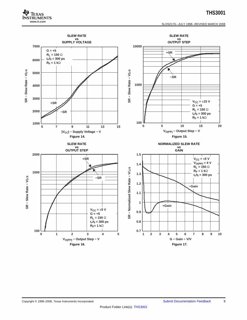
SLEW RATE SLEW RATEvs vs
SUPPLY VOLTAGE OUTPUT STEP
Figure 14. Figure 15.
SLEW RATE NORMALIZED SLEW RATEvs vs
OUTPUT STEP GAIN
Figure 16. Figure 17.
Copyright © 1998–2008, Texas Instruments Incorporated Submit Documentation Feedback 9
Product Folder Link(s): THS3001
www.ti.com
VO(PP) − Peak-to-Peak Output V oltage Swing − V
0 2 4 6 12 14108 16
−55
−65
−75
−85
−60
−70
−80
−50
18
2nd Harmonic
3rd Harmonic
Har
mon
ic D
isto
rtion
− d
Bc
20
8 MHzGain = 2VCC = ±15 VRL = 150 ΩRF = 750 Ω
VO(PP) − Peak-to-Peak Output V oltage Swing − V
0 2 4 6 12 14108 16
−65
−75
−85
−95
−70
−80
−90
−50
18
2nd Harmonic
3rd Harmonic
Har
mon
ic D
isto
rtion
− d
Bc
20
4 MHzGain = 2VCC = ±15 VRL = 150 ΩRF = 750 Ω
−55
−60
−70
−80
−90
−100
−75
−85
−95
2nd Harmonic
3rd Harmonic
Har
mon
ic D
isto
rtion
− d
Bc
Gain = 2VCC = ±15 VVO = 2 VPPRL = 150 ΩRF = 750 Ω
100k 1M 10M
f − Frequency − Hz
−70
−80
−90
−100
−75
−85
−95
2nd Harmonic
3rd Harmonic
Har
mon
ic D
isto
rtion
− d
Bc
Gain = 2VCC = ±5 VVO = 2 VPPRL = 150 ΩRF = 750 Ω
100k 1M 10M
f − Frequency − Hz
−60
−65
THS3001
SLOS217G–JULY 1998–REVISED MARCH 2008
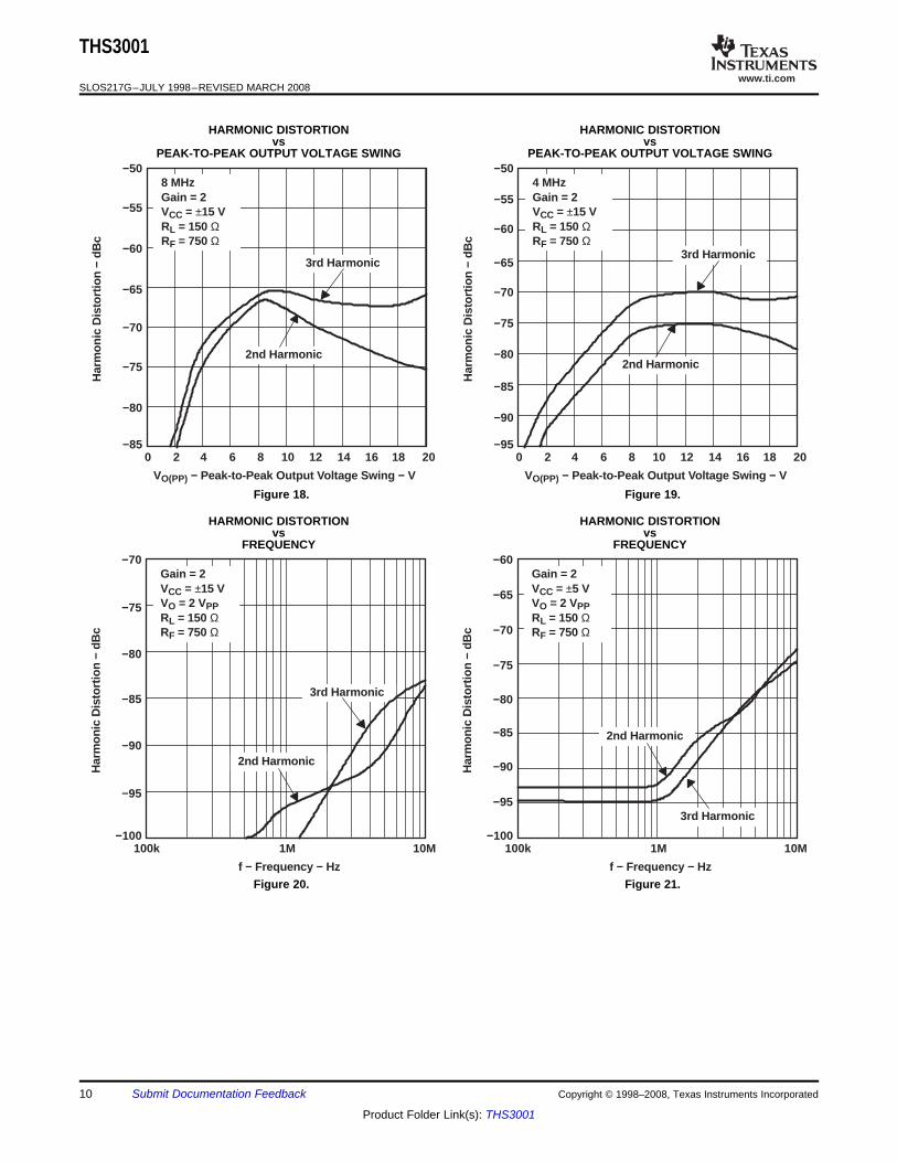
HARMONIC DISTORTION HARMONIC DISTORTIONvs vs
PEAK-TO-PEAK OUTPUT VOLTAGE SWING PEAK-TO-PEAK OUTPUT VOLTAGE SWING
Figure 18. Figure 19.
HARMONIC DISTORTION HARMONIC DISTORTIONvs vs
FREQUENCY FREQUENCY
Figure 20. Figure 21.
10 Submit Documentation Feedback Copyright © 1998–2008, Texas Instruments Incorporated
Product Folder Link(s): THS3001
www.ti.com
1 2 3 4 7 8
Number of 150 Ω Loads
65
VCC = ±15 V
0.04
0.02
0
0.03
0.01
VCC = ±5 V
Diff
eren
tial G
ain
− %
Gain = 2RF = 750 Ω40 IRE NTSC ModulationWorst Case: ±100 IRE Ramp
1 2 3 4 7 8
Number of 150 Ω Loads
65
VCC = ±15 V
0.04
0.02
0
0.03
0.01
VCC = ±5 V
Diff
eren
tial G
ain
− %
Gain = 2RF = 750 Ω40 IRE PAL ModulationWorst Case: ±100 IRE Ramp
1 2 3 4 7 8
Number of 150 Ω Loads
65
VCC = ±15 V
0.3
0.1
0
0.15
0.05
VCC = ±5 VDiff
eren
tial P
hase
− D
egre
es
Gain = 2RF = 750 Ω40 IRE NTSC ModulationWorst Case: ±100 IRE Ramp
0.2
0.25
1 2 3 4 7 8
Number of 150 Ω Loads
65
VCC = ±15 V
0.35
0.1
0
0.15
0.05
VCC = ±5 VDiff
eren
tial P
hase
− D
egre
es
Gain = 2RF = 750 Ω40 IRE PAL ModulationWorst Case: ±100 IRE Ramp
0.2
0.25
0.3
THS3001
SLOS217G–JULY 1998–REVISED MARCH 2008
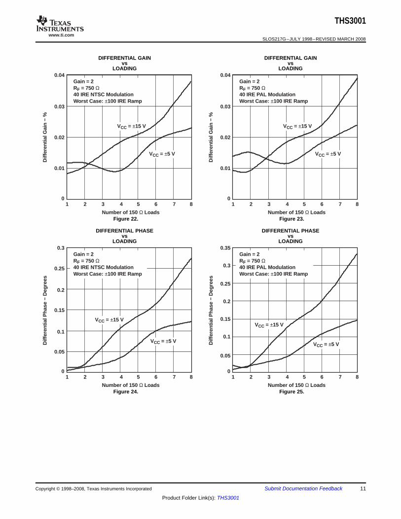
DIFFERENTIAL GAIN DIFFERENTIAL GAINvs vs
LOADING LOADING
Figure 22. Figure 23.
DIFFERENTIAL PHASE DIFFERENTIAL PHASEvs vs
LOADING LOADING
Figure 24. Figure 25.
Copyright © 1998–2008, Texas Instruments Incorporated Submit Documentation Feedback 11
Product Folder Link(s): THS3001
www.ti.com
f − Frequency − Hz
0
−2
−4
−61M 100M
1
−1
−3
−5
10M 1G100k
2
3
RF = 750 Ω
Out
put
Am
plitu
de −
dB
RF = 1.5 kΩ
Gain = 1VCC = ±15 VRL = 150 ΩVI = 200 mV RMS
RF = 1 kΩ
f − Frequency − Hz
0
−2
−4
−61M 100M
1
−1
−3
−5
10M 1G100k
2
3
RF = 750 Ω
Out
put
Am
plitu
de −
dB
RF = 1.5 kΩ
Gain = 1VCC = ±5 VRL = 150 ΩVI = 200 mV RMS
RF = 1 kΩ
f − Frequency − Hz
5
3
1
−11M 100M
6
4
2
0
10M 1G100k
7
8RF = 560 Ω
Out
put
Am
plitu
de −
dB
RF = 1 kΩ
Gain = 2VCC = ±15 VRL = 150 ΩVI = 200 mV RMS
RF = 680 Ω
9
f − Frequency − Hz
5
3
1
−11M 100M
6
4
2
0
10M 1G100k
7
8RF = 560 Ω
Out
put
Am
plitu
de −
dB
RF = 1 kΩ
Gain = 2VCC = ±5 VRL = 150 ΩVI = 200 mV RMS
RF = 750 Ω
9
THS3001
SLOS217G–JULY 1998–REVISED MARCH 2008
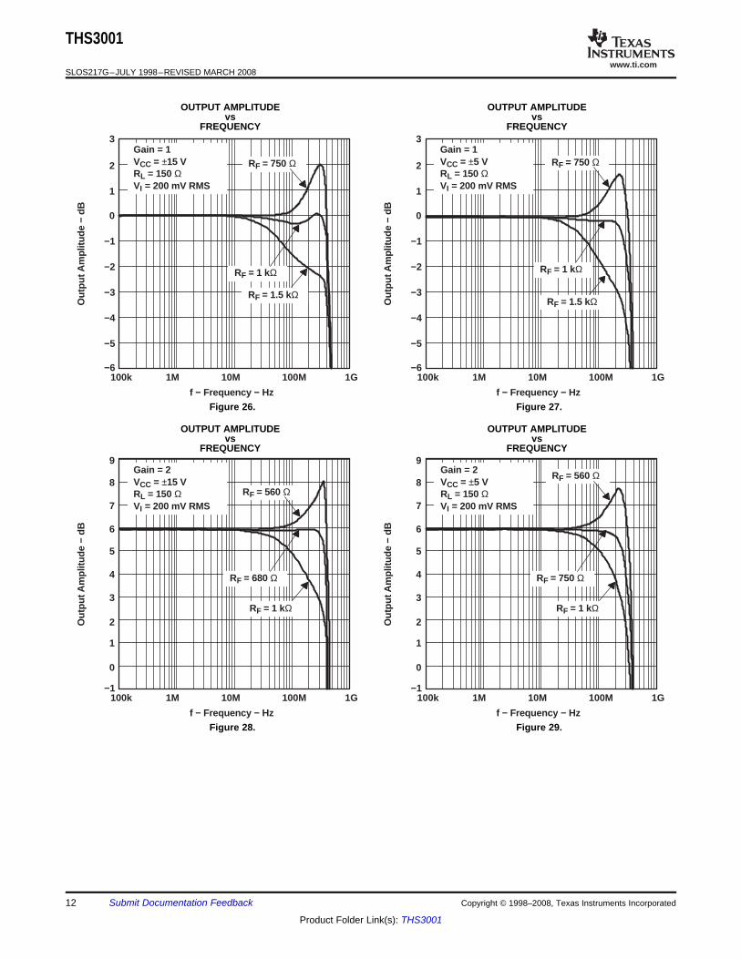
OUTPUT AMPLITUDE OUTPUT AMPLITUDEvs vs
FREQUENCY FREQUENCY
Figure 26. Figure 27.
OUTPUT AMPLITUDE OUTPUT AMPLITUDEvs vs
FREQUENCY FREQUENCY
Figure 28. Figure 29.
12 Submit Documentation Feedback Copyright © 1998–2008, Texas Instruments Incorporated
Product Folder Link(s): THS3001
www.ti.com
f − Frequency − Hz
50
30
10
−101M 100M
60
40
20
0
10M 1G100k
70
G = +1000RF = 10 kΩRL = 150 ΩVO = 200 mV RMS
VCC = ±5 V
VCC = ±15 V
Out
put
Am
plitu
de −
dB
f − Frequency − Hz
0
−2
−4
−61M 100M
1
−1
−3
−5
10M 1G100k
2
3
RF = 560 Ω
Nor
mal
ized
Out
put R
espo
nse
− dB
RF = 680 Ω
RF = 1 kΩ
Gain = −1VCC = ±15 VRL = 150 ΩVI = 200 mV RMS
f − Frequency − Hz
0
−2
−4
−61M 100M
1
−1
−3
−5
10M 1G100k
2
3
RF = 560 Ω
Nor
mal
ized
Out
put R
espo
nse
− dB
RF = 750 Ω
RF = 1 kΩ
Gain = −1VCC = ±5 VRL = 150 ΩVI = 200 mV RMS
THS3001
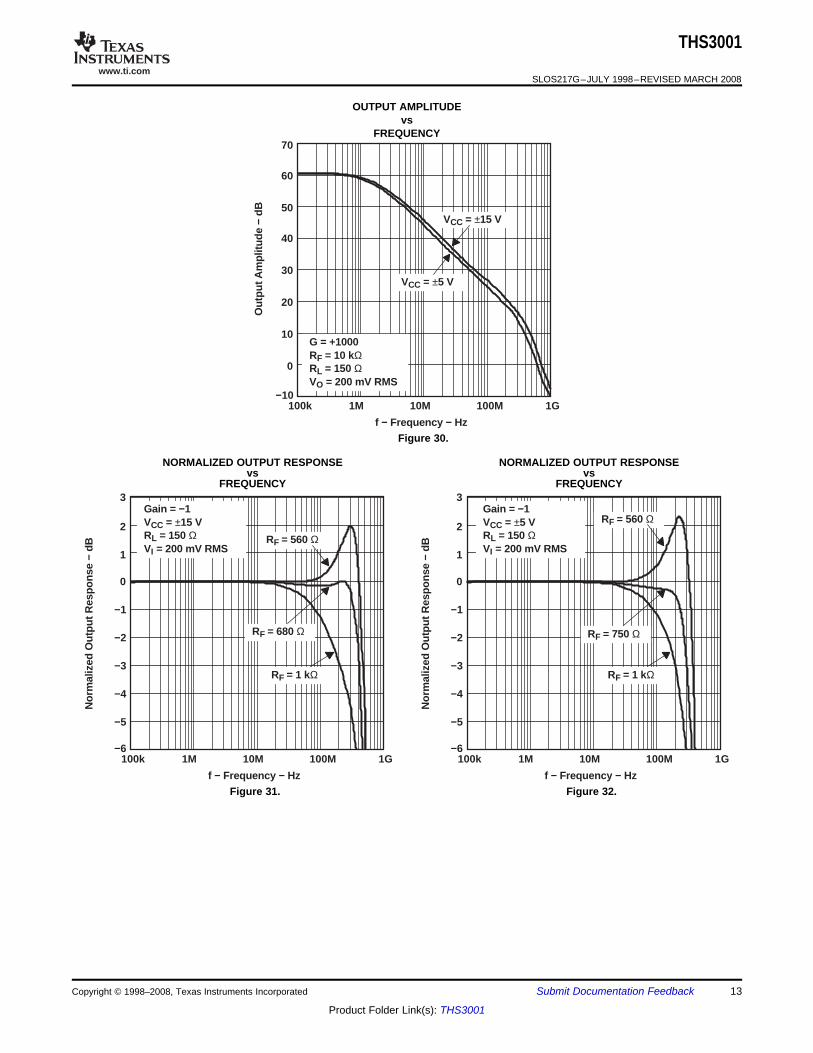
SLOS217G–JULY 1998–REVISED MARCH 2008
OUTPUT AMPLITUDEvs
FREQUENCY
Figure 30.
NORMALIZED OUTPUT RESPONSE NORMALIZED OUTPUT RESPONSEvs vs
FREQUENCY FREQUENCY
Figure 31. Figure 32.
Copyright © 1998–2008, Texas Instruments Incorporated Submit Documentation Feedback 13
Product Folder Link(s): THS3001
www.ti.com
f − Frequency − Hz
3
−3
−9
−151M 100M
0
−6
−12
10M 1G100k
Gain = +5VCC = ±15 VRL = 150 ΩVO = 200 mV RMS
RF = 390 Ω
Nor
mal
ized
Out
put R
espo
nse
− dB
RF = 560 Ω
RF = 1 kΩ
f − Frequency − Hz
−2
−6
−10
−141M 100M
0
−4
−8
−12
10M 1G100k
2
4
Gain = +5VCC = ±5 VRL = 150 ΩVO = 200 mV RMS
RF = 390 Ω
Nor
mal
ized
Out
put R
espo
nse
− dB
RF = 620 Ω
RF = 1 kΩ
f − Frequency − Hz
−12
−18
−24
−301M 100M
−9
−15
−21
−27
10M 1G100k
−6
−3
Gain = 1VCC = ±15 VRF = 1 kΩRL = 150 Ω
VI = 500 mV
VI = 250 mV
VI = 125 mV
VI = 62.5 mV
Out
put L
evel
− d
BV
f − Frequency − Hz
−6
−12
−18
−241M 100M
−3
−9
−15
−21
10M 1G100k
0
3
Out
put L
evel
− d
BV
Gain = 2VCC = ±15 VRF = 680 ΩRL = 150 Ω
VI = 500 mV
VI = 250 mV
VI = 125 mV
VI = 62.5 mV
THS3001
SLOS217G–JULY 1998–REVISED MARCH 2008
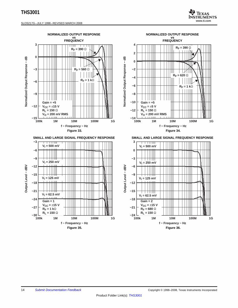
NORMALIZED OUTPUT RESPONSE NORMALIZED OUTPUT RESPONSEvs vs
FREQUENCY FREQUENCY
Figure 33. Figure 34.
SMALL AND LARGE SIGNAL FREQUENCY RESPONSE SMALL AND LARGE SIGNAL FREQUENCY RESPONSE
Figure 35. Figure 36.
14 Submit Documentation Feedback Copyright © 1998–2008, Texas Instruments Incorporated
Product Folder Link(s): THS3001
www.ti.com
t − Time − ns
Gain = 1VCC = ±5 VRL = 150 ΩRF = 1 kΩtr/tf = 300 ps
−200
0
100
−100
100
−100
0 302010 40 50 7060 80 90 100
300
−200
−300
− O
utpu
t Vol
tage
− V
VO
VI
− In
put V
olta
ge −
mV
200
t − Time − ns
Gain = 5VCC = ±5 VRL = 150 ΩRF = 1 kΩtr/tf = 300 ps
−60
0
100
−100
20
−20
0 302010 40 50 7060 80 90 100
60
−200
−300
− O
utpu
t Vol
tage
− m
VV
OV
I−
Inpu
t Vol
tage
− m
V
200
t − Time − ns
Gain = +1VCC = ±15 VRL = 150 ΩRF = 1 kΩtr/tf= 2.5 ns
−3
0
1
−1
1
−1
0 302010 40 50 7060 80 90 100
3
−2
−3
− O
utpu
t Vol
tage
− V
VO
VI
− In
put V
olta
ge −
V
2
t − Time − ns
Gain = 1VCC = ±5 VRL = 150 ΩRF = 1 kΩtr/tf= 2.5 ns
−3
0
1
−1
1
−1
0 302010 40 50 7060 80 90 100
3
−2
−3
− O
utpu
t Vol
tage
− V
VO
VI
− In
put V
olta
ge −
V
2
THS3001
SLOS217G–JULY 1998–REVISED MARCH 2008
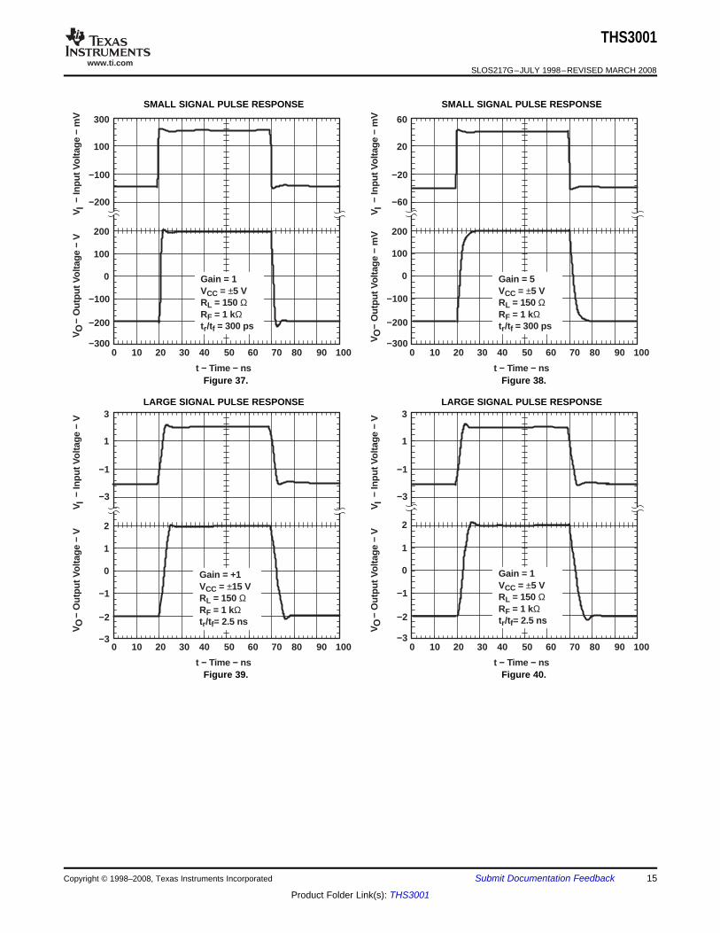
SMALL SIGNAL PULSE RESPONSE SMALL SIGNAL PULSE RESPONSE
Figure 37. Figure 38.
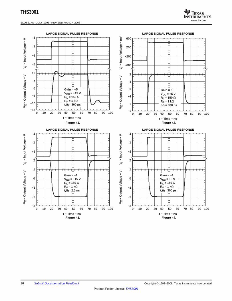
LARGE SIGNAL PULSE RESPONSE LARGE SIGNAL PULSE RESPONSE
Figure 39. Figure 40.
Copyright © 1998–2008, Texas Instruments Incorporated Submit Documentation Feedback 15
Product Folder Link(s): THS3001
www.ti.com
t − Time − ns
Gain = +5VCC = ±15 VRL = 150 ΩRF = 1 kΩtr/tf= 300 ps
−3
0
5
−5
1
−1
0 302010 40 50 7060 80 90 100
3
−10
−15
− O
utpu
t Vol
tage
− V
VO
VI
− In
put V
olta
ge −
V
10
t − Time − ns
Gain = 5VCC = ±5 VRL = 150 ΩRF = 1 kΩtr/tf= 300 ps
−600
0
1
−1
200
−200
0 302010 40 50 7060 80 90 100
600
−2
−3
− O
utpu
t Vol
tage
− V
VO
VI
− In
put V
olta
ge −
mV
2
t − Time − ns
Gain = −1VCC = ±15 VRL = 150 ΩRF = 1 kΩtr/tf= 2.5 ns
2
0
1
−1
1
−1
0 302010 40 50 7060 80 90 100
3
−2
−3
− O
utpu
t Vol
tage
− V
VO
VI
− In
put V
olta
ge −
V
t − Time − ns
Gain = −1VCC = ±5 VRL = 150 ΩRF = 1 kΩtr/tf= 300 ps
2
0
1
−1
1
−1
0 302010 40 50 7060 80 90 100
3
−2
−3
− O
utpu
t Vol
tage
− V
VO
VI
− In
put V
olta
ge −
V
THS3001
SLOS217G–JULY 1998–REVISED MARCH 2008
LARGE SIGNAL PULSE RESPONSE LARGE SIGNAL PULSE RESPONSE
Figure 41. Figure 42.
LARGE SIGNAL PULSE RESPONSE LARGE SIGNAL PULSE RESPONSE
Figure 43. Figure 44.
16 Submit Documentation Feedback Copyright © 1998–2008, Texas Instruments Incorporated
Product Folder Link(s): THS3001
www.ti.com
t − Time − ns
Gain = −5VCC = ±15 VRL = 150 ΩRF = 1 kΩtr/tf= 300 ps
−2
0
5
−5
1
−1
0 302010 40 50 7060 80 90 100
3
−10
−15
− O
utpu
t Vol
tage
− V
VO
VI
− In
put V
olta
ge −
V
10
t − Time − ns
Gain = −5VCC = ±5 VRL = 150 ΩRF = 1 kΩtr/tf= 300 ps
−600
0
1
−1
200
−200
0 302010 40 50 7060 80 90 100
600
−2
−3
− O
utpu
t Vol
tage
− V
VO
VI
− In
put V
olta
ge −
mV
2
THS3001
SLOS217G–JULY 1998–REVISED MARCH 2008
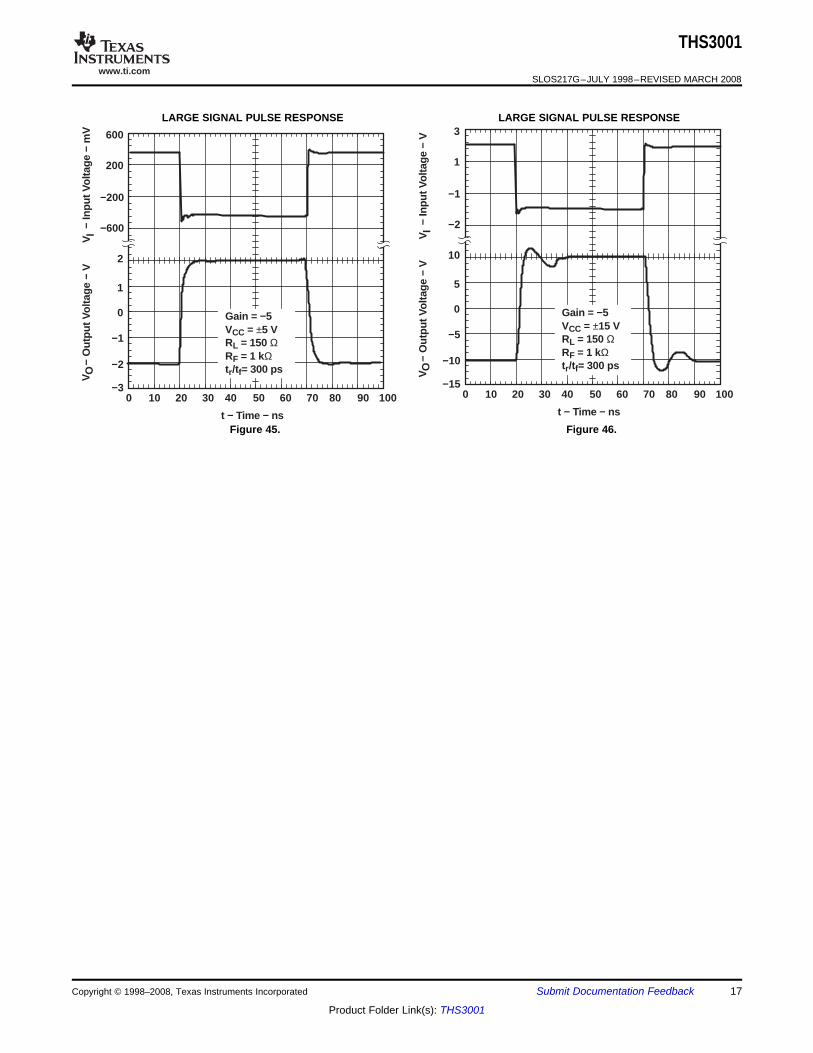
LARGE SIGNAL PULSE RESPONSE LARGE SIGNAL PULSE RESPONSE
Figure 45. Figure 46.
Copyright © 1998–2008, Texas Instruments Incorporated Submit Documentation Feedback 17
Product Folder Link(s): THS3001
www.ti.com
APPLICATION INFORMATION
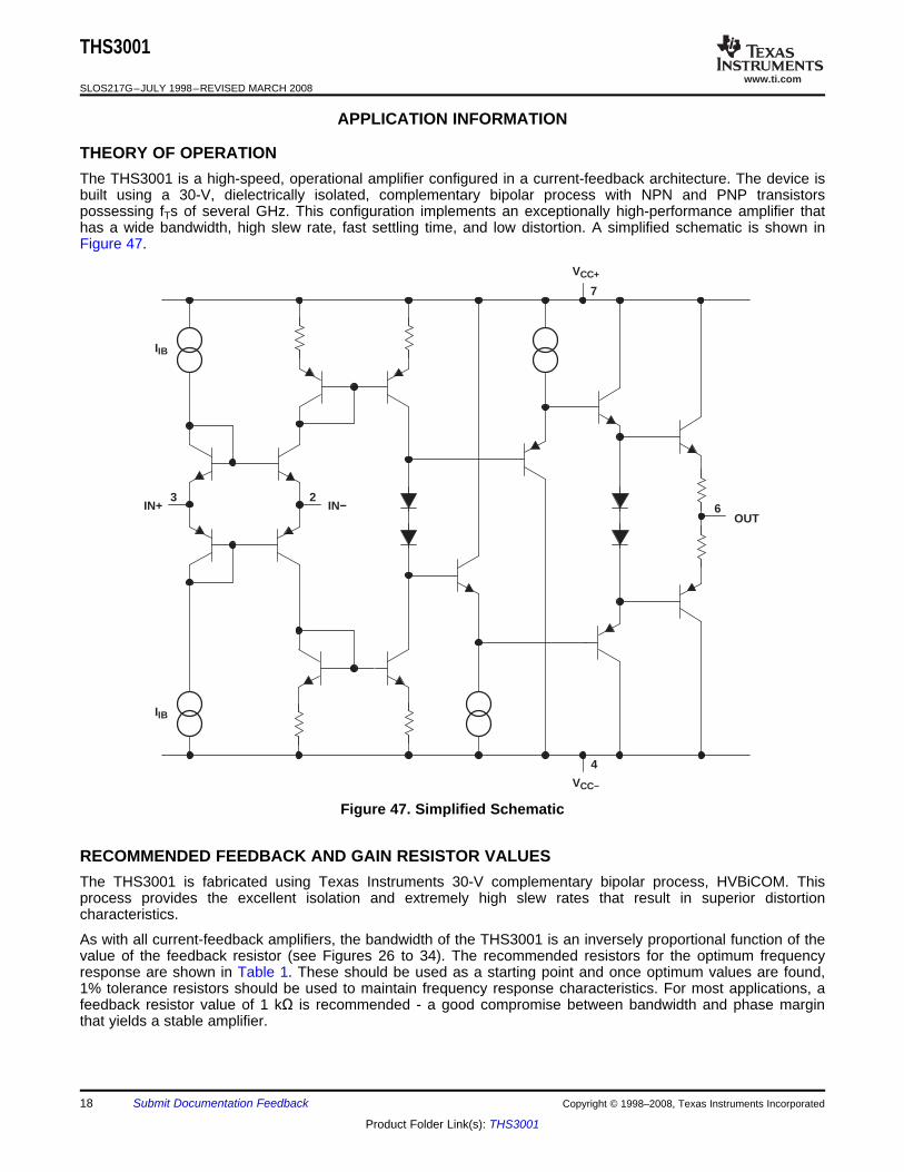
THEORY OF OPERATION
IN+ IN−
VCC+
VCC−
OUT
3 26
7
4
IIB
IIB
RECOMMENDED FEEDBACK AND GAIN RESISTOR VALUES
THS3001
SLOS217G–JULY 1998–REVISED MARCH 2008
The THS3001 is a high-speed, operational amplifier configured in a current-feedback architecture. The device isbuilt using a 30-V, dielectrically isolated, complementary bipolar process with NPN and PNP transistorspossessing fTs of several GHz. This configuration implements an exceptionally high-performance amplifier thathas a wide bandwidth, high slew rate, fast settling time, and low distortion. A simplified schematic is shown inFigure 47.
Figure 47. Simplified Schematic
The THS3001 is fabricated using Texas Instruments 30-V complementary bipolar process, HVBiCOM. Thisprocess provides the excellent isolation and extremely high slew rates that result in superior distortioncharacteristics.
As with all current-feedback amplifiers, the bandwidth of the THS3001 is an inversely proportional function of thevalue of the feedback resistor (see Figures 26 to 34). The recommended resistors for the optimum frequencyresponse are shown in Table 1. These should be used as a starting point and once optimum values are found,1% tolerance resistors should be used to maintain frequency response characteristics. For most applications, afeedback resistor value of 1 kΩ is recommended - a good compromise between bandwidth and phase marginthat yields a stable amplifier.
18 Submit Documentation Feedback Copyright © 1998–2008, Texas Instruments Incorporated
Product Folder Link(s): THS3001
www.ti.com
OFFSET VOLTAGE
THS3001
SLOS217G–JULY 1998–REVISED MARCH 2008
Consistent with current-feedback amplifiers, increasing the gain is best accomplished by changing the gainresistor, not the feedback resistor. This is because the bandwidth of the amplifier is dominated by the feedbackresistor value and internal dominant-pole capacitor. The ability to control the amplifier gain independent of thebandwidth constitutes a major advantage of current-feedback amplifiers over conventional voltage-feedbackamplifiers. Therefore, once a frequency response is found suitable to a particular application, adjust the value ofthe gain resistor to increase or decrease the overall amplifier gain.
Finally, it is important to realize the effects of the feedback resistance on distortion. Increasing the resistancedecreases the loop gain and increases the distortion. It is also important to know that decreasing load impedanceincreases total harmonic distortion (THD). Typically, the third-order harmonic distortion increases more than thesecond-order harmonic distortion.
Table 1. Recommended Resistor Values for OptimumFrequency Response
GAIN RF for VCC = ±15 V RF for VCC = ±5 V1 1 kΩ 1 kΩ
2, -1 680 Ω 750 Ω2 620 Ω 620 Ω5 560 Ω 620 Ω
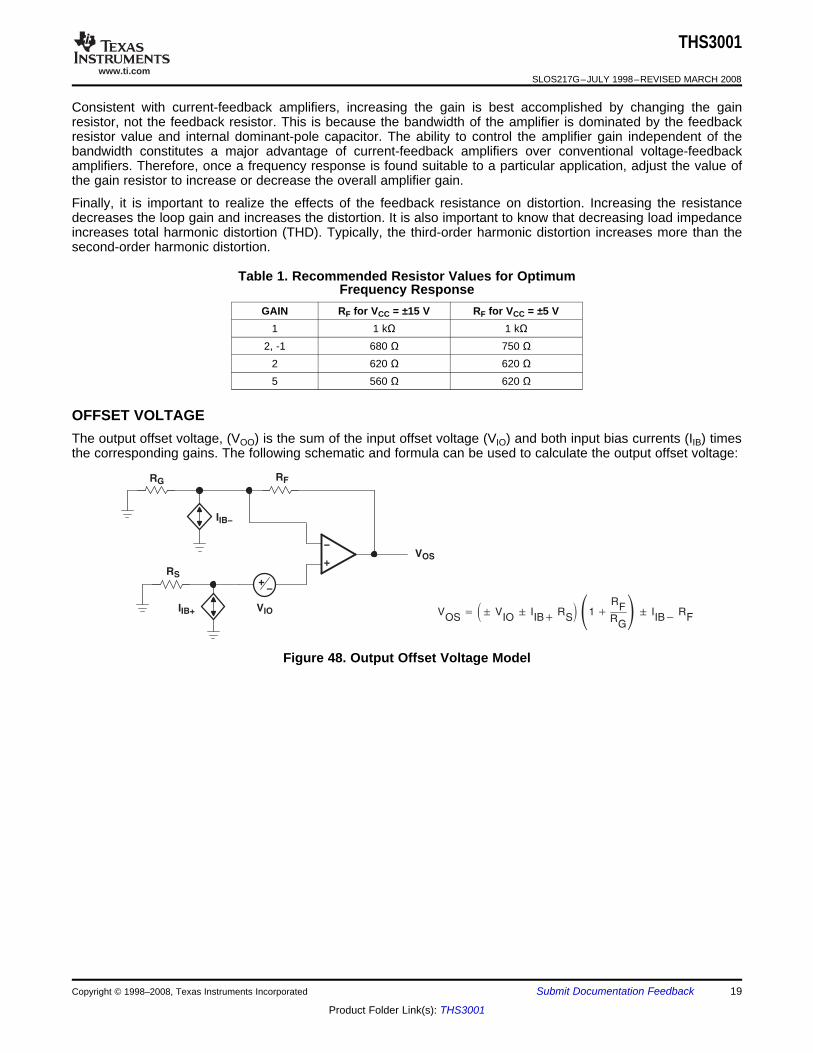
The output offset voltage, (VOO) is the sum of the input offset voltage (VIO) and both input bias currents (IIB) timesthe corresponding gains. The following schematic and formula can be used to calculate the output offset voltage:
Figure 48. Output Offset Voltage Model
Copyright © 1998–2008, Texas Instruments Incorporated Submit Documentation Feedback 19
Product Folder Link(s): THS3001
www.ti.com
NOISE CALCULATIONS
_+
RF
RS
RG
eRg
eRf
eRs en
IN+
Noiseless
IN−
enieno
eni en
2 IN RS
2 IN– RF RG2 4 kTRs 4 kTRF RG
Where:
k = Boltzmann’s constant = 1.380658 × 10⁻²³
T = Temperature in degrees Kelvin (273 +°C)RF || RG = Parallel resistance of RF and RG
eno eni AV eni1 RFRG (Noninverting Case)
THS3001
SLOS217G–JULY 1998–REVISED MARCH 2008
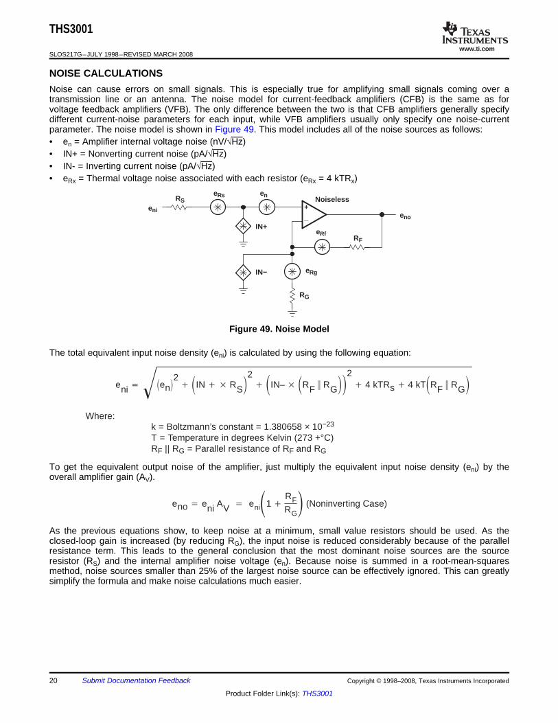
Noise can cause errors on small signals. This is especially true for amplifying small signals coming over atransmission line or an antenna. The noise model for current-feedback amplifiers (CFB) is the same as forvoltage feedback amplifiers (VFB). The only difference between the two is that CFB amplifiers generally specifydifferent current-noise parameters for each input, while VFB amplifiers usually only specify one noise-currentparameter. The noise model is shown in Figure 49. This model includes all of the noise sources as follows:• en = Amplifier internal voltage noise (nV/√Hz)• IN+ = Nonverting current noise (pA/√Hz)• IN- = Inverting current noise (pA/√Hz)• eRx = Thermal voltage noise associated with each resistor (eRx = 4 kTRx)
Figure 49. Noise Model
The total equivalent input noise density (eni) is calculated by using the following equation:
To get the equivalent output noise of the amplifier, just multiply the equivalent input noise density (eni) by theoverall amplifier gain (AV).
As the previous equations show, to keep noise at a minimum, small value resistors should be used. As theclosed-loop gain is increased (by reducing RG), the input noise is reduced considerably because of the parallelresistance term. This leads to the general conclusion that the most dominant noise sources are the sourceresistor (RS) and the internal amplifier noise voltage (en). Because noise is summed in a root-mean-squaresmethod, noise sources smaller than 25% of the largest noise source can be effectively ignored. This can greatlysimplify the formula and make noise calculations much easier.
20 Submit Documentation Feedback Copyright © 1998–2008, Texas Instruments Incorporated
Product Folder Link(s): THS3001
www.ti.com
SLEW RATE
t − Time − ns
SR = 1500 V/µsGain = 5VCC = ±15 VRL = 150 ΩRF = 1 kΩtr/tf = 10 ns
10
0
5
−5
2
0
0 604020 80 100 140120 160 180 200
4
−10
−15
− O
utpu
t Vol
tage
− V
VO
VI
− In
put V
olta
ge −
V
t − Time − ns
SR = 2400 V/µsGain = 5VCC = ±15 VRL = 150 ΩRF = 1 kΩtr/tf = 5 ns
−2
0
5
−5
2
0
0 604020 80 100 140120 160 180 200
4
−10
−15
− O
utpu
t Vol
tage
− V
VO
VI
− In
put V
olta
ge −
V
THS3001
SLOS217G–JULY 1998–REVISED MARCH 2008
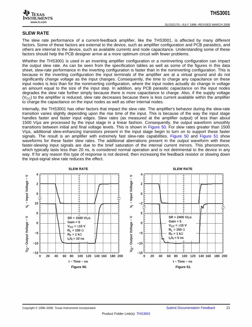
The slew rate performance of a current-feedback amplifier, like the THS3001, is affected by many differentfactors. Some of these factors are external to the device, such as amplifier configuration and PCB parasitics, andothers are internal to the device, such as available currents and node capacitance. Understanding some of thesefactors should help the PCB designer arrive at a more optimum circuit with fewer problems.
Whether the THS3001 is used in an inverting amplifier configuration or a noninverting configuration can impactthe output slew rate. As can be seen from the specification tables as well as some of the figures in this datasheet, slew-rate performance in the inverting configuration is faster than in the noninverting configuration. This isbecause in the inverting configuration the input terminals of the amplifier are at a virtual ground and do notsignificantly change voltage as the input changes. Consequently, the time to charge any capacitance on theseinput nodes is less than for the noninverting configuration, where the input nodes actually do change in voltagean amount equal to the size of the input step. In addition, any PCB parasitic capacitance on the input nodesdegrades the slew rate further simply because there is more capacitance to charge. Also, if the supply voltage(VCC) to the amplifier is reduced, slew rate decreases because there is less current available within the amplifierto charge the capacitance on the input nodes as well as other internal nodes.
Internally, the THS3001 has other factors that impact the slew rate. The amplifier's behavior during the slew-ratetransition varies slightly depending upon the rise time of the input. This is because of the way the input stagehandles faster and faster input edges. Slew rates (as measured at the amplifier output) of less than about1500 V/µs are processed by the input stage in a linear fashion. Consequently, the output waveform smoothlytransitions between initial and final voltage levels. This is shown in Figure 50. For slew rates greater than 1500V/µs, additional slew-enhancing transistors present in the input stage begin to turn on to support these fastersignals. The result is an amplifier with extremely fast slew-rate capabilities. Figure 50 and Figure 51 showwaveforms for these faster slew rates. The additional aberrations present in the output waveform with thesefaster-slewing input signals are due to the brief saturation of the internal current mirrors. This phenomenon,which typically lasts less than 20 ns, is considered normal operation and is not detrimental to the device in anyway. If for any reason this type of response is not desired, then increasing the feedback resistor or slowing downthe input-signal slew rate reduces the effect.
SLEW RATE SLEW RATE
Figure 50. Figure 51.
Copyright © 1998–2008, Texas Instruments Incorporated Submit Documentation Feedback 21
Product Folder Link(s): THS3001
www.ti.com
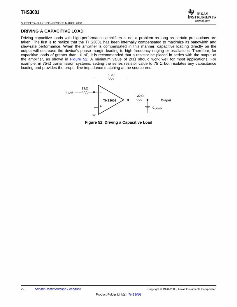
DRIVING A CAPACITIVE LOAD
+
_
THS3001
CLOAD
1 kΩ
Input
Output
1 kΩ
20 Ω
THS3001
SLOS217G–JULY 1998–REVISED MARCH 2008
Driving capacitive loads with high-performance amplifiers is not a problem as long as certain precautions aretaken. The first is to realize that the THS3001 has been internally compensated to maximize its bandwidth andslew-rate performance. When the amplifier is compensated in this manner, capacitive loading directly on theoutput will decrease the device's phase margin leading to high-frequency ringing or oscillations. Therefore, forcapacitive loads of greater than 10 pF, it is recommended that a resistor be placed in series with the output ofthe amplifier, as shown in Figure 52. A minimum value of 20Ω should work well for most applications. Forexample, in 75-Ω transmission systems, setting the series resistor value to 75 Ω both isolates any capacitanceloading and provides the proper line impedance matching at the source end.
Figure 52. Driving a Capacitive Load
22 Submit Documentation Feedback Copyright © 1998–2008, Texas Instruments Incorporated
Product Folder Link(s): THS3001
www.ti.com
PCB DESIGN CONSIDERATIONS
−2
−4
−6
−81M
f − Frequency − Hz
−1
−3
−5
−7
100k 10M 100M
0
Out
put
Am
plitu
de −
dB
1
1G
Gain = −1VCC = ±15 VVO = 200 mV RMS
CI = 10 pF
CI = Stray C Only
+
−
1 kΩ
RL =150 Ω
Cin
Vin
Vout
1 kΩ
50 Ω
2
0
−2
−41M
f − Frequency − Hz
3
1
−1
−3
100k 10M 100M
4
6
Out
put
Am
plitu
de −
dB
5
7
1G
Gain = 1VCC = ±15 VVO = 200 mV RMS
CI = 1 pF
CI = 0 pF(Stray C Only)
+
−
1 kΩ
50 ΩRL =
150 Ω
Cin
Vin
Vout
THS3001
SLOS217G–JULY 1998–REVISED MARCH 2008
Proper PCB design techniques in two areas are important to ensure proper operation of the THS3001. Theseareas are high-speed layout techniques and thermal-management techniques. Because the THS3001 is ahigh-speed part, the following guidelines are recommended.• Ground plane - It is essential that a ground plane be used on the board to provide all components with a low
inductive ground connection, but should be removed from below the output and negative input pins as notedbelow.
• The DGN package option includes a thermal pad for increased thermal performance. When using thispackage, it is recommended to distribute the negative supply as a power plane, and tie the thermal pad to thissupply with multiple vias for proper power dissipation. It is not recommended to tie the thermal pad to groundwhen using split supply (±V) as this will cause worse distortion performance than shown in this data sheet.
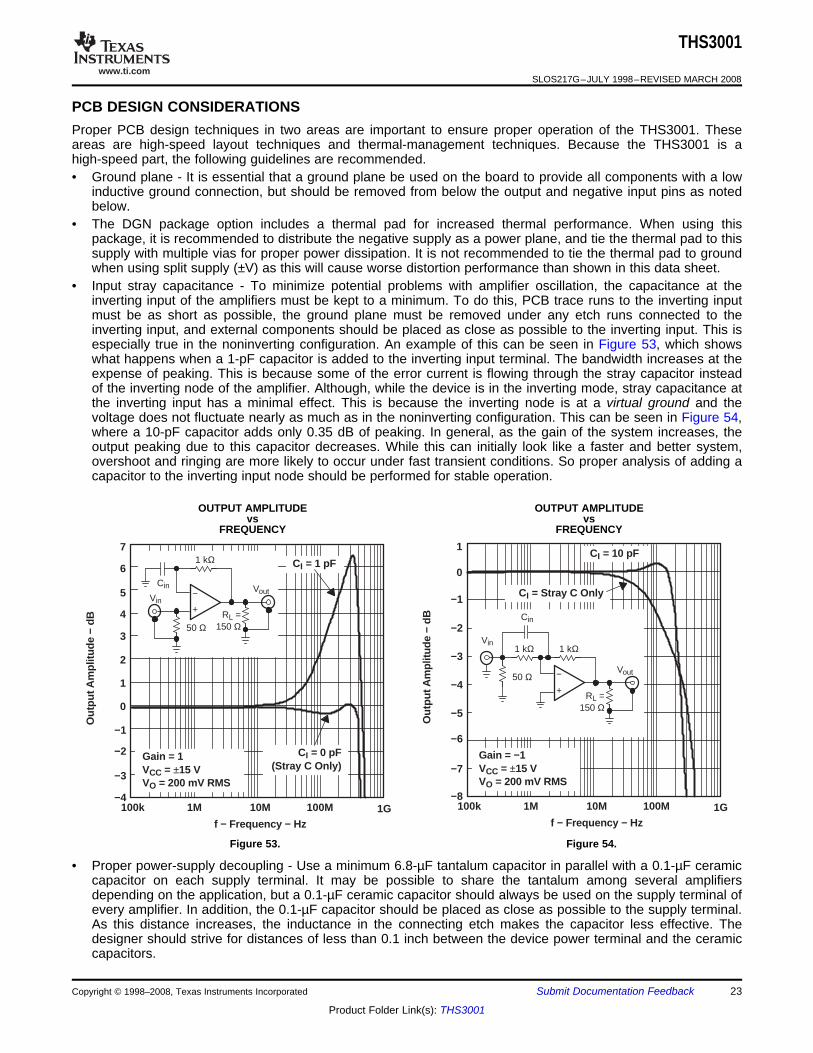
• Input stray capacitance - To minimize potential problems with amplifier oscillation, the capacitance at theinverting input of the amplifiers must be kept to a minimum. To do this, PCB trace runs to the inverting inputmust be as short as possible, the ground plane must be removed under any etch runs connected to theinverting input, and external components should be placed as close as possible to the inverting input. This isespecially true in the noninverting configuration. An example of this can be seen in Figure 53, which showswhat happens when a 1-pF capacitor is added to the inverting input terminal. The bandwidth increases at theexpense of peaking. This is because some of the error current is flowing through the stray capacitor insteadof the inverting node of the amplifier. Although, while the device is in the inverting mode, stray capacitance atthe inverting input has a minimal effect. This is because the inverting node is at a virtual ground and thevoltage does not fluctuate nearly as much as in the noninverting configuration. This can be seen in Figure 54,where a 10-pF capacitor adds only 0.35 dB of peaking. In general, as the gain of the system increases, theoutput peaking due to this capacitor decreases. While this can initially look like a faster and better system,overshoot and ringing are more likely to occur under fast transient conditions. So proper analysis of adding acapacitor to the inverting input node should be performed for stable operation.
OUTPUT AMPLITUDE OUTPUT AMPLITUDEvs vs
FREQUENCY FREQUENCY
Figure 53. Figure 54.
• Proper power-supply decoupling - Use a minimum 6.8-µF tantalum capacitor in parallel with a 0.1-µF ceramiccapacitor on each supply terminal. It may be possible to share the tantalum among several amplifiersdepending on the application, but a 0.1-µF ceramic capacitor should always be used on the supply terminal ofevery amplifier. In addition, the 0.1-µF capacitor should be placed as close as possible to the supply terminal.As this distance increases, the inductance in the connecting etch makes the capacitor less effective. Thedesigner should strive for distances of less than 0.1 inch between the device power terminal and the ceramiccapacitors.
Copyright © 1998–2008, Texas Instruments Incorporated Submit Documentation Feedback 23
Product Folder Link(s): THS3001
www.ti.com
THERMAL INFORMATION
PD TMAX–TAJA
Where:
PD = Maximum power dissipation of THS3001 (watts)TMAX = Absolute maximum junction temperature (150°C)TA = Free-ambient air temperature (°C)θJA = Thermal coefficient from die junction to ambient air (°C/W)
TA − Free-Air T emperature − °C
1
0−20 20
1.5
0.5
0 40 100−40 60 80
P D−
Max
imum
Pow
er D
issi
patio
n −
W
SOIC-D Package:θJA = 169°C/WTJ = 150°CNo Airflow
GENERAL CONFIGURATIONS
THS3001
SLOS217G–JULY 1998–REVISED MARCH 2008
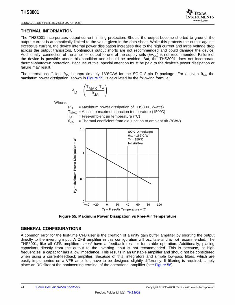
The THS3001 incorporates output-current-limiting protection. Should the output become shorted to ground, theoutput current is automatically limited to the value given in the data sheet. While this protects the output againstexcessive current, the device internal power dissipation increases due to the high current and large voltage dropacross the output transistors. Continuous output shorts are not recommended and could damage the device.Additionally, connection of the amplifier output to one of the supply rails (±VCC) is not recommended. Failure ofthe device is possible under this condition and should be avoided. But, the THS3001 does not incorporatethermal-shutdown protection. Because of this, special attention must be paid to the device's power dissipation orfailure may result.
The thermal coefficient θJA is approximately 169°C/W for the SOIC 8-pin D package. For a given θJA, themaximum power dissipation, shown in Figure 55, is calculated by the following formula:
Figure 55. Maximum Power Dissipation vs Free-Air Temperature
A common error for the first-time CFB user is the creation of a unity gain buffer amplifier by shorting the outputdirectly to the inverting input. A CFB amplifier in this configuration will oscillate and is not recommended. TheTHS3001, like all CFB amplifiers, must have a feedback resistor for stable operation. Additionally, placingcapacitors directly from the output to the inverting input is not recommended. This is because, at highfrequencies, a capacitor has a low impedance. This results in an unstable amplifier and should not be consideredwhen using a current-feedback amplifier. Because of this, integrators and simple low-pass filters, which areeasily implemented on a VFB amplifier, have to be designed slightly differently. If filtering is required, simplyplace an RC-filter at the noninverting terminal of the operational-amplifier (see Figure 56).
24 Submit Documentation Feedback Copyright © 1998–2008, Texas Instruments Incorporated
Product Folder Link(s): THS3001
www.ti.com
VIVO
C1
+
−
RG RF
R1
f3 dB 12R1C1
VOVI
1RFRG 1
1 sR1C1
VI
C2R2R1
C1
RFRG
R1 = R2 = RC1 = C2 = CQ = Peaking Factor(Butterworth Q = 0.707)
(=
1Q
2 − )RG
RF
_+
f3 dB
12RC
+
−
C1RF
RG
VOVI
THS3001
VOVI
RFRG
S 1RFC1
S
THS3001
SLOS217G–JULY 1998–REVISED MARCH 2008
Figure 56. Single-Pole Low-Pass Filter
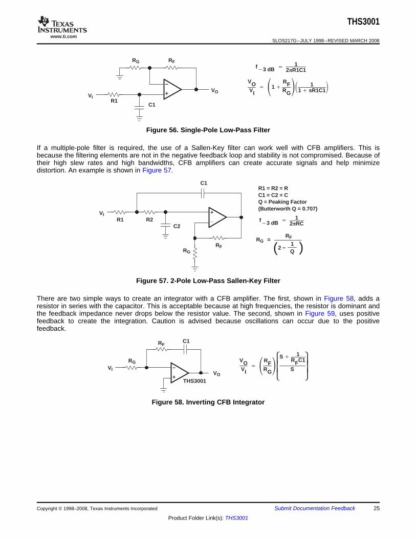
If a multiple-pole filter is required, the use of a Sallen-Key filter can work well with CFB amplifiers. This isbecause the filtering elements are not in the negative feedback loop and stability is not compromised. Because oftheir high slew rates and high bandwidths, CFB amplifiers can create accurate signals and help minimizedistortion. An example is shown in Figure 57.
Figure 57. 2-Pole Low-Pass Sallen-Key Filter
There are two simple ways to create an integrator with a CFB amplifier. The first, shown in Figure 58, adds aresistor in series with the capacitor. This is acceptable because at high frequencies, the resistor is dominant andthe feedback impedance never drops below the resistor value. The second, shown in Figure 59, uses positivefeedback to create the integration. Caution is advised because oscillations can occur due to the positivefeedback.
Figure 58. Inverting CFB Integrator
Copyright © 1998–2008, Texas Instruments Incorporated Submit Documentation Feedback 25
Product Folder Link(s): THS3001
www.ti.com
+
−
RF
VO
RG
R2R1
C1RA
VI
THS3001
For Stable Operation:
R2
R1 || RA≥
RF
RG
sR1C1( )
RF
RG1 +
VO ≅ VI
+
−
750 Ω750 Ω
75 Ω75 Ω
75 Ω
75 Ω
75 Ω
N Lines
VO1
VON
THS3001
75-Ω Transmission Line
VI
THS3001
SLOS217G–JULY 1998–REVISED MARCH 2008
Figure 59. Noninverting CFB Integrator
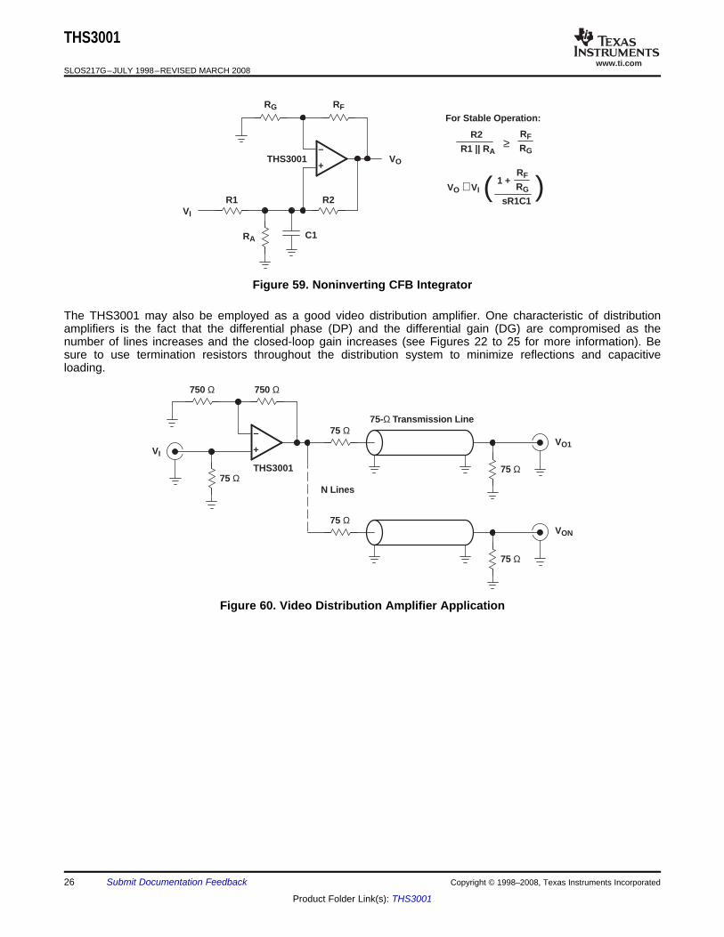
The THS3001 may also be employed as a good video distribution amplifier. One characteristic of distributionamplifiers is the fact that the differential phase (DP) and the differential gain (DG) are compromised as thenumber of lines increases and the closed-loop gain increases (see Figures 22 to 25 for more information). Besure to use termination resistors throughout the distribution system to minimize reflections and capacitiveloading.
Figure 60. Video Distribution Amplifier Application
26 Submit Documentation Feedback Copyright © 1998–2008, Texas Instruments Incorporated
Product Folder Link(s): THS3001
www.ti.com
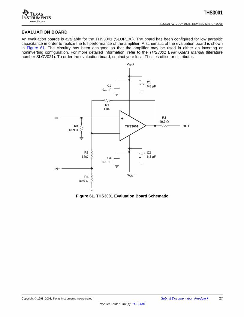
EVALUATION BOARD
_
+
THS3001
VCC−
VCC+
C36.8 µFC4
0.1 µF
C16.8 µFC2
0.1 µF
R11 kΩ
R51 kΩ
R349.9 Ω
R249.9 Ω
R449.9 Ω
IN−
IN+
OUT
+
+
THS3001
SLOS217G–JULY 1998–REVISED MARCH 2008
An evaluation boards is available for the THS3001 (SLOP130). The board has been configured for low parasiticcapacitance in order to realize the full performance of the amplifier. A schematic of the evaluation board is shownin Figure 61. The circuitry has been designed so that the amplifier may be used in either an inverting ornoninverting configuration. For more detailed information, refer to the THS3001 EVM User's Manual (literaturenumber SLOV021). To order the evaluation board, contact your local TI sales office or distributor.
Figure 61. THS3001 Evaluation Board Schematic
Copyright © 1998–2008, Texas Instruments Incorporated Submit Documentation Feedback 27
Product Folder Link(s): THS3001
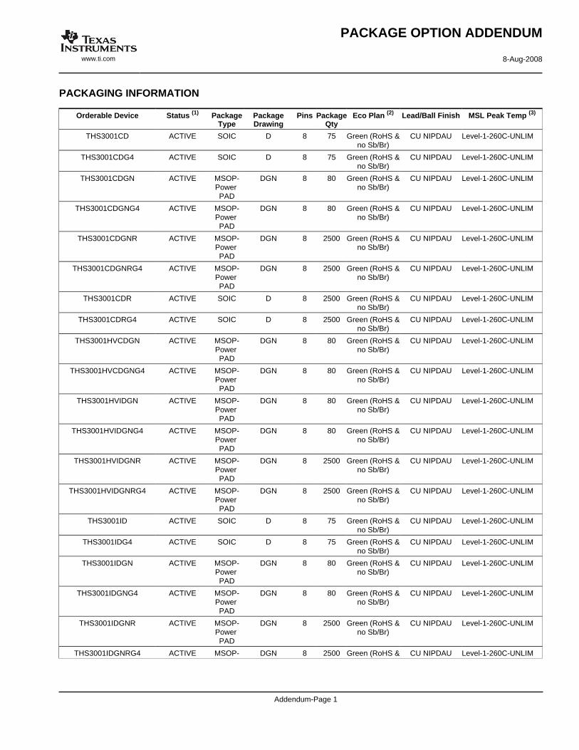
PACKAGING INFORMATION
Orderable Device Status (1) PackageType
PackageDrawing
Pins PackageQty
Eco Plan (2) Lead/Ball Finish MSL Peak Temp (3)
THS3001CD ACTIVE SOIC D 8 75 Green (RoHS &no Sb/Br)
CU NIPDAU Level-1-260C-UNLIM
THS3001CDG4 ACTIVE SOIC D 8 75 Green (RoHS &no Sb/Br)
CU NIPDAU Level-1-260C-UNLIM
THS3001CDGN ACTIVE MSOP-Power PAD
DGN 8 80 Green (RoHS &no Sb/Br)
CU NIPDAU Level-1-260C-UNLIM
THS3001CDGNG4 ACTIVE MSOP-Power PAD
DGN 8 80 Green (RoHS &no Sb/Br)
CU NIPDAU Level-1-260C-UNLIM
THS3001CDGNR ACTIVE MSOP-Power PAD
DGN 8 2500 Green (RoHS &no Sb/Br)
CU NIPDAU Level-1-260C-UNLIM
THS3001CDGNRG4 ACTIVE MSOP-Power PAD
DGN 8 2500 Green (RoHS &no Sb/Br)
CU NIPDAU Level-1-260C-UNLIM
THS3001CDR ACTIVE SOIC D 8 2500 Green (RoHS &no Sb/Br)
CU NIPDAU Level-1-260C-UNLIM
THS3001CDRG4 ACTIVE SOIC D 8 2500 Green (RoHS &no Sb/Br)
CU NIPDAU Level-1-260C-UNLIM
THS3001HVCDGN ACTIVE MSOP-Power PAD
DGN 8 80 Green (RoHS &no Sb/Br)
CU NIPDAU Level-1-260C-UNLIM
THS3001HVCDGNG4 ACTIVE MSOP-Power PAD
DGN 8 80 Green (RoHS &no Sb/Br)
CU NIPDAU Level-1-260C-UNLIM
THS3001HVIDGN ACTIVE MSOP-Power PAD
DGN 8 80 Green (RoHS &no Sb/Br)
CU NIPDAU Level-1-260C-UNLIM
THS3001HVIDGNG4 ACTIVE MSOP-Power PAD
DGN 8 80 Green (RoHS &no Sb/Br)
CU NIPDAU Level-1-260C-UNLIM
THS3001HVIDGNR ACTIVE MSOP-Power PAD
DGN 8 2500 Green (RoHS &no Sb/Br)
CU NIPDAU Level-1-260C-UNLIM
THS3001HVIDGNRG4 ACTIVE MSOP-Power PAD
DGN 8 2500 Green (RoHS &no Sb/Br)
CU NIPDAU Level-1-260C-UNLIM
THS3001ID ACTIVE SOIC D 8 75 Green (RoHS &no Sb/Br)
CU NIPDAU Level-1-260C-UNLIM
THS3001IDG4 ACTIVE SOIC D 8 75 Green (RoHS &no Sb/Br)
CU NIPDAU Level-1-260C-UNLIM
THS3001IDGN ACTIVE MSOP-Power PAD
DGN 8 80 Green (RoHS &no Sb/Br)
CU NIPDAU Level-1-260C-UNLIM
THS3001IDGNG4 ACTIVE MSOP-Power PAD
DGN 8 80 Green (RoHS &no Sb/Br)
CU NIPDAU Level-1-260C-UNLIM
THS3001IDGNR ACTIVE MSOP-Power PAD
DGN 8 2500 Green (RoHS &no Sb/Br)
CU NIPDAU Level-1-260C-UNLIM
THS3001IDGNRG4 ACTIVE MSOP- DGN 8 2500 Green (RoHS & CU NIPDAU Level-1-260C-UNLIM
PACKAGE OPTION ADDENDUM
www.ti.com 8-Aug-2008
Addendum-Page 1
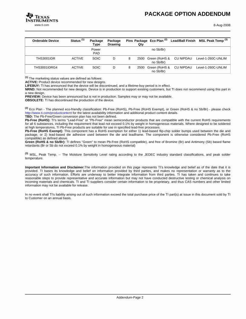
Orderable Device Status (1) PackageType
PackageDrawing
Pins PackageQty
Eco Plan (2) Lead/Ball Finish MSL Peak Temp (3)
Power PAD
no Sb/Br)
THS3001IDR ACTIVE SOIC D 8 2500 Green (RoHS &no Sb/Br)
CU NIPDAU Level-1-260C-UNLIM
THS3001IDRG4 ACTIVE SOIC D 8 2500 Green (RoHS &no Sb/Br)
CU NIPDAU Level-1-260C-UNLIM
(1) The marketing status values are defined as follows:ACTIVE: Product device recommended for new designs.LIFEBUY: TI has announced that the device will be discontinued, and a lifetime-buy period is in effect.NRND: Not recommended for new designs. Device is in production to support existing customers, but TI does not recommend using this part ina new design.PREVIEW: Device has been announced but is not in production. Samples may or may not be available.OBSOLETE: TI has discontinued the production of the device.
(2) Eco Plan - The planned eco-friendly classification: Pb-Free (RoHS), Pb-Free (RoHS Exempt), or Green (RoHS & no Sb/Br) - please checkhttp://www.ti.com/productcontent for the latest availability information and additional product content details.TBD: The Pb-Free/Green conversion plan has not been defined.Pb-Free (RoHS): TI's terms "Lead-Free" or "Pb-Free" mean semiconductor products that are compatible with the current RoHS requirementsfor all 6 substances, including the requirement that lead not exceed 0.1% by weight in homogeneous materials. Where designed to be solderedat high temperatures, TI Pb-Free products are suitable for use in specified lead-free processes.Pb-Free (RoHS Exempt): This component has a RoHS exemption for either 1) lead-based flip-chip solder bumps used between the die andpackage, or 2) lead-based die adhesive used between the die and leadframe. The component is otherwise considered Pb-Free (RoHScompatible) as defined above.Green (RoHS & no Sb/Br): TI defines "Green" to mean Pb-Free (RoHS compatible), and free of Bromine (Br) and Antimony (Sb) based flameretardants (Br or Sb do not exceed 0.1% by weight in homogeneous material)
(3) MSL, Peak Temp. -- The Moisture Sensitivity Level rating according to the JEDEC industry standard classifications, and peak soldertemperature.
Important Information and Disclaimer:The information provided on this page represents TI's knowledge and belief as of the date that it isprovided. TI bases its knowledge and belief on information provided by third parties, and makes no representation or warranty as to theaccuracy of such information. Efforts are underway to better integrate information from third parties. TI has taken and continues to takereasonable steps to provide representative and accurate information but may not have conducted destructive testing or chemical analysis onincoming materials and chemicals. TI and TI suppliers consider certain information to be proprietary, and thus CAS numbers and other limitedinformation may not be available for release.
In no event shall TI's liability arising out of such information exceed the total purchase price of the TI part(s) at issue in this document sold by TIto Customer on an annual basis.
PACKAGE OPTION ADDENDUM
www.ti.com 8-Aug-2008
Addendum-Page 2
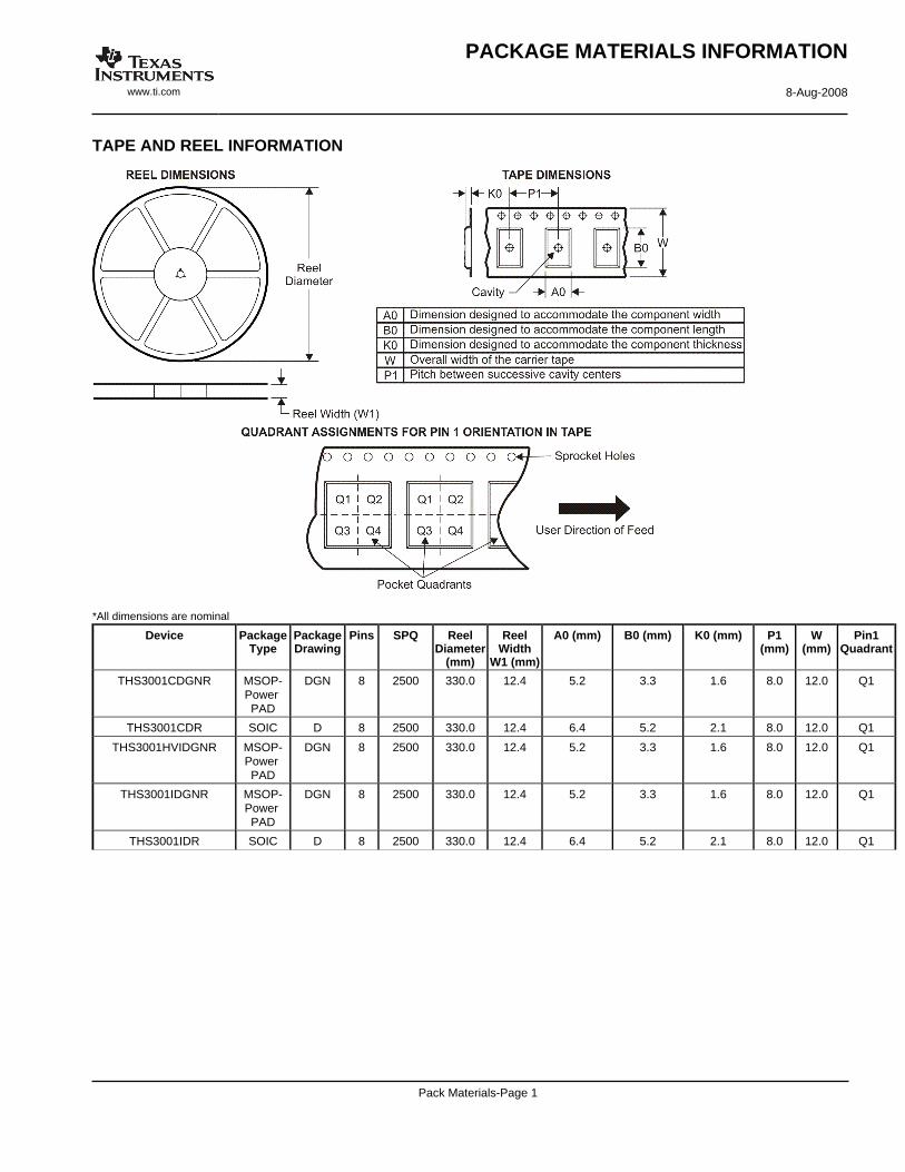
TAPE AND REEL INFORMATION
*All dimensions are nominal
Device PackageType
PackageDrawing
Pins SPQ ReelDiameter
(mm)
ReelWidth
W1 (mm)
A0 (mm) B0 (mm) K0 (mm) P1(mm)
W(mm)
Pin1Quadrant
THS3001CDGNR MSOP-Power PAD
DGN 8 2500 330.0 12.4 5.2 3.3 1.6 8.0 12.0 Q1
THS3001CDR SOIC D 8 2500 330.0 12.4 6.4 5.2 2.1 8.0 12.0 Q1
THS3001HVIDGNR MSOP-Power PAD
DGN 8 2500 330.0 12.4 5.2 3.3 1.6 8.0 12.0 Q1
THS3001IDGNR MSOP-Power PAD
DGN 8 2500 330.0 12.4 5.2 3.3 1.6 8.0 12.0 Q1
THS3001IDR SOIC D 8 2500 330.0 12.4 6.4 5.2 2.1 8.0 12.0 Q1
PACKAGE MATERIALS INFORMATION
www.ti.com 8-Aug-2008
Pack Materials-Page 1
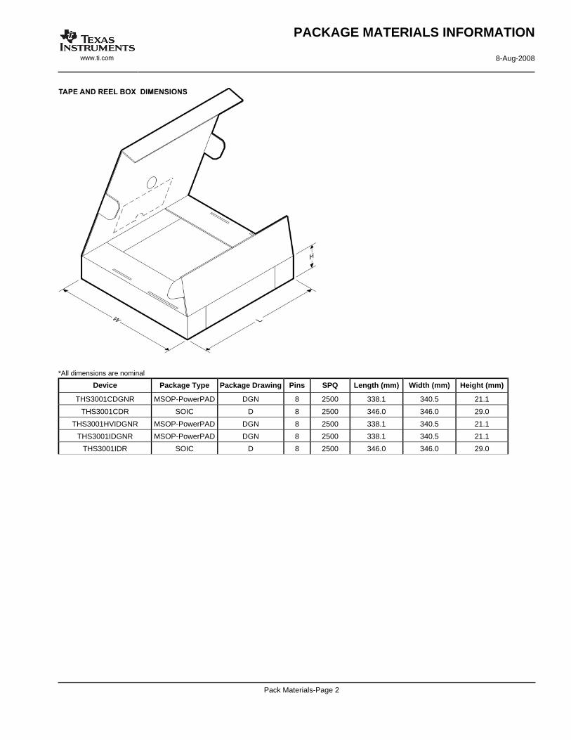
*All dimensions are nominal
Device Package Type Package Drawing Pins SPQ Length (mm) Width (mm) Height (mm)
THS3001CDGNR MSOP-PowerPAD DGN 8 2500 338.1 340.5 21.1
THS3001CDR SOIC D 8 2500 346.0 346.0 29.0
THS3001HVIDGNR MSOP-PowerPAD DGN 8 2500 338.1 340.5 21.1
THS3001IDGNR MSOP-PowerPAD DGN 8 2500 338.1 340.5 21.1
THS3001IDR SOIC D 8 2500 346.0 346.0 29.0
PACKAGE MATERIALS INFORMATION
www.ti.com 8-Aug-2008
Pack Materials-Page 2
IMPORTANT NOTICETexas Instruments Incorporated and its subsidiaries (TI) reserve the right to make corrections, modifications, enhancements, improvements,and other changes to its products and services at any time and to discontinue any product or service without notice. Customers shouldobtain the latest relevant information before placing orders and should verify that such information is current and complete. All products aresold subject to TI’s terms and conditions of sale supplied at the time of order acknowledgment.TI warrants performance of its hardware products to the specifications applicable at the time of sale in accordance with TI’s standardwarranty. Testing and other quality control techniques are used to the extent TI deems necessary to support this warranty. Except wheremandated by government requirements, testing of all parameters of each product is not necessarily performed.TI assumes no liability for applications assistance or customer product design. Customers are responsible for their products andapplications using TI components. To minimize the risks associated with customer products and applications, customers should provideadequate design and operating safeguards.TI does not warrant or represent that any license, either express or implied, is granted under any TI patent right, copyright, mask work right,or other TI intellectual property right relating to any combination, machine, or process in which TI products or services are used. Informationpublished by TI regarding third-party products or services does not constitute a license from TI to use such products or services or awarranty or endorsement thereof. Use of such information may require a license from a third party under the patents or other intellectualproperty of the third party, or a license from TI under the patents or other intellectual property of TI.Reproduction of TI information in TI data books or data sheets is permissible only if reproduction is without alteration and is accompaniedby all associated warranties, conditions, limitations, and notices. Reproduction of this information with alteration is an unfair and deceptivebusiness practice. TI is not responsible or liable for such altered documentation. Information of third parties may be subject to additionalrestrictions.Resale of TI products or services with statements different from or beyond the parameters stated by TI for that product or service voids allexpress and any implied warranties for the associated TI product or service and is an unfair and deceptive business practice. TI is notresponsible or liable for any such statements.TI products are not authorized for use in safety-critical applications (such as life support) where a failure of the TI product would reasonablybe expected to cause severe personal injury or death, unless officers of the parties have executed an agreement specifically governingsuch use. Buyers represent that they have all necessary expertise in the safety and regulatory ramifications of their applications, andacknowledge and agree that they are solely responsible for all legal, regulatory and safety-related requirements concerning their productsand any use of TI products in such safety-critical applications, notwithstanding any applications-related information or support that may beprovided by TI. Further, Buyers must fully indemnify TI and its representatives against any damages arising out of the use of TI products insuch safety-critical applications.TI products are neither designed nor intended for use in military/aerospace applications or environments unless the TI products arespecifically designated by TI as military-grade or "enhanced plastic." Only products designated by TI as military-grade meet militaryspecifications. Buyers acknowledge and agree that any such use of TI products which TI has not designated as military-grade is solely atthe Buyer's risk, and that they are solely responsible for compliance with all legal and regulatory requirements in connection with such use.TI products are neither designed nor intended for use in automotive applications or environments unless the specific TI products aredesignated by TI as compliant with ISO/TS 16949 requirements. Buyers acknowledge and agree that, if they use any non-designatedproducts in automotive applications, TI will not be responsible for any failure to meet such requirements.Following are URLs where you can obtain information on other Texas Instruments products and application solutions:Products ApplicationsAmplifiers amplifier.ti.com Audio www.ti.com/audioData Converters dataconverter.ti.com Automotive www.ti.com/automotiveDLP® Products www.dlp.com Broadband www.ti.com/broadbandDSP dsp.ti.com Digital Control www.ti.com/digitalcontrolClocks and Timers www.ti.com/clocks Medical www.ti.com/medicalInterface interface.ti.com Military www.ti.com/militaryLogic logic.ti.com Optical Networking www.ti.com/opticalnetworkPower Mgmt power.ti.com Security www.ti.com/securityMicrocontrollers microcontroller.ti.com Telephony www.ti.com/telephonyRFID www.ti-rfid.com Video & Imaging www.ti.com/videoRF/IF and ZigBee® Solutions www.ti.com/lprf Wireless www.ti.com/wireless
Mailing Address: Texas Instruments, Post Office Box 655303, Dallas, Texas 75265Copyright © 2009, Texas Instruments Incorporated