TPS24720 2.5-V to 18-V High-Efficiency Adjustable Power ... · tps24720 r 2 m sense! m csd16403q5 1...
41
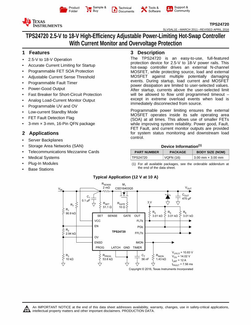
TPS24720 R 2 m SENSE Ω M CSD16403Q5 1 C T 56 nF VCC OUT GATE SENSE PGb PROG TIMER GND OV EN R 2.94 2 kΩ R 90.9 k 1 Ω R 3 10 kΩ R 5 3.01 kΩ LATCH IMON R 4 3.01 kΩ FLTb FFLTb R 6 3.01 kΩ ENSD SET R SET 51.1 Ω R PROG 53.6 kΩ R IMON 1.43 kΩ V UVLO OV LMT FAULT = 10.83 V V = 14.02 V I = 12 A t = 7.56 ms C 1 0.1 F μ R 7 C OUT 470 F μ V IN V OUT 3V R GATE 10 Ω Copyright © 2016, Texas Instruments Incorporated Product Folder Sample & Buy Technical Documents Tools & Software Support & Community An IMPORTANT NOTICE at the end of this data sheet addresses availability, warranty, changes, use in safety-critical applications, intellectual property matters and other important disclaimers. PRODUCTION DATA. TPS24720 SLVSAL1E – MARCH 2011 – REVISED APRIL 2016 TPS24720 2.5-V to 18-V High-Efficiency Adjustable Power-Limiting Hot-Swap Controller With Current Monitor and Overvoltage Protection 1 1 Features 1• 2.5-V to 18-V Operation • Accurate Current Limiting for Startup • Programmable FET SOA Protection • Adjustable Current Sense Threshold • Programmable Fault Timer • Power-Good Output • Fast Breaker for Short-Circuit Protection • Analog Load-Current Monitor Output • Programmable UV and OV • Low-current Standby Mode • FET Fault Detection Flag • 3-mm × 3-mm, 16-Pin QFN package 2 Applications • Server Backplanes • Storage Area Networks (SAN) • Telecommunications Mezzanine Cards • Medical Systems • Plug-In Modules • Base Stations 3 Description The TPS24720 is an easy-to-use, full-featured protection device for 2.5-V to 18-V power rails. This hot-swap controller drives an external N-channel MOSFET, while protecting source, load and external MOSFET against multiple potentially damaging events. During startup, load current and MOSFET power dissipation are limited to user-selected values. After startup, currents above the user-selected limit will be allowed to flow until programmed timeout – except in extreme overload events when load is immediately disconnected from source. Programmable power limiting ensures the external MOSFET operates inside its safe operating area (SOA) at all times. This allows use of smaller FETs while improving system reliability. Power good, Fault, FET Fault, and current monitor outputs are provided for system status monitoring and downstream load control. Device Information (1) PART NUMBER PACKAGE BODY SIZE (NOM) TPS24720 VQFN (16) 3.00 mm × 3.00 mm (1) For all available packages, see the orderable addendum at the end of the data sheet. Typical Application (12 V at 10 A)
Transcript of TPS24720 2.5-V to 18-V High-Efficiency Adjustable Power ... · tps24720 r 2 m sense! m csd16403q5 1...
TPS24720
R
2 mSENSE
ΩM
CSD16403Q51
CT
56 nF
VCC
OUTGATESENSE
PGb
PROG TIMERGND
OV
EN
R
2.942
kΩ
R
90.9 k1
Ω
R3
10 kΩ
R5
3.01 kΩ
LATCH
IMON
R4
3.01 kΩ
FLTb
FFLTb
R6
3.01 kΩ
ENSD
SET
RSET
51.1 Ω
RPROG
53.6 kΩ
RIMON
1.43 kΩ
VUVLO
OV
LMT
FAULT
= 10.83 V
V = 14.02 V
I = 12 A
t = 7.56 ms
C1
0.1 Fμ
R7
COUT
470 Fμ
VINVOUT
3 VRGATE
10 Ω
Copyright © 2016, Texas Instruments Incorporated
Product
Folder
Sample &Buy
Technical
Documents
Tools &
Software
Support &Community
An IMPORTANT NOTICE at the end of this data sheet addresses availability, warranty, changes, use in safety-critical applications,intellectual property matters and other important disclaimers. PRODUCTION DATA.
TPS24720SLVSAL1E –MARCH 2011–REVISED APRIL 2016
TPS24720 2.5-V to 18-V High-Efficiency Adjustable Power-Limiting Hot-Swap ControllerWith Current Monitor and Overvoltage Protection
1
1 Features1• 2.5-V to 18-V Operation• Accurate Current Limiting for Startup• Programmable FET SOA Protection• Adjustable Current Sense Threshold• Programmable Fault Timer• Power-Good Output• Fast Breaker for Short-Circuit Protection• Analog Load-Current Monitor Output• Programmable UV and OV• Low-current Standby Mode• FET Fault Detection Flag• 3-mm × 3-mm, 16-Pin QFN package
2 Applications• Server Backplanes• Storage Area Networks (SAN)• Telecommunications Mezzanine Cards• Medical Systems• Plug-In Modules• Base Stations
3 DescriptionThe TPS24720 is an easy-to-use, full-featuredprotection device for 2.5-V to 18-V power rails. Thishot-swap controller drives an external N-channelMOSFET, while protecting source, load and externalMOSFET against multiple potentially damagingevents. During startup, load current and MOSFETpower dissipation are limited to user-selected values.After startup, currents above the user-selected limitwill be allowed to flow until programmed timeout –except in extreme overload events when load isimmediately disconnected from source.
Programmable power limiting ensures the externalMOSFET operates inside its safe operating area(SOA) at all times. This allows use of smaller FETswhile improving system reliability. Power good, Fault,FET Fault, and current monitor outputs are providedfor system status monitoring and downstream loadcontrol.
Device Information(1)
PART NUMBER PACKAGE BODY SIZE (NOM)TPS24720 VQFN (16) 3.00 mm × 3.00 mm
(1) For all available packages, see the orderable addendum atthe end of the data sheet.
Typical Application (12 V at 10 A)
2
TPS24720SLVSAL1E –MARCH 2011–REVISED APRIL 2016 www.ti.com
Product Folder Links: TPS24720
Submit Documentation Feedback Copyright © 2011–2016, Texas Instruments Incorporated
Table of Contents1 Features .................................................................. 12 Applications ........................................................... 13 Description ............................................................. 14 Revision History..................................................... 25 Pin Configuration and Functions ......................... 46 Specifications......................................................... 5
6.1 Absolute Maximum Ratings ...................................... 56.2 ESD Ratings ............................................................ 56.3 THERMAL INFORMATION....................................... 56.4 Recommended Operating Conditions....................... 56.5 Electrical Characteristics........................................... 66.6 Timing Requirements ................................................ 86.7 Typical Characteristics .............................................. 9
7 Detailed Description ............................................ 137.1 Overview ................................................................. 137.2 Functional Block Diagram ....................................... 13
7.3 Feature Description................................................. 137.4 Device Functional Modes........................................ 17
8 Application and Implementation ........................ 248.1 Application Information............................................ 248.2 Typical Application .................................................. 24
9 Power Supply Recommendations ...................... 3010 Layout................................................................... 31
10.1 Layout Guidelines ................................................. 3110.2 Layout Example .................................................... 31
11 Device and Documentation Support ................. 3211.1 Documentation Support ....................................... 3211.2 Trademarks ........................................................... 3211.3 Electrostatic Discharge Caution............................ 3211.4 Glossary ................................................................ 32
12 Mechanical, Packaging, and OrderableInformation ........................................................... 32
4 Revision HistoryNOTE: Page numbers for previous revisions may differ from page numbers in the current version.
Changes from Revision D (March 2015) to Revision E Page
• Changed the Part Number From TPS247120 To: TPS24720 in the Device Information table.............................................. 1
Changes from Revision C (September 2013) to Revision D Page
• Added ESD Rating table, Feature Description section, Device Functional Modes, Application and Implementationsection, Power Supply Recommendations section, Layout section, Device and Documentation Support section, andMechanical, Packaging, and Orderable Information section. ................................................................................................ 1
• Changed the Input voltage range, PROG - MAX value in the Absolute Maximum Ratings table From: 0.3 To: 3.6 ............ 5• Deleted External capacitance - GATE from the Recommended Operating Conditions ......................................................... 5• Deleted text from the last paragraph in the GATE section "If used, any capacitor connecting GATE and GND should
not exceed 1 μF and it should be connected in series with a resistor of no less than 1 kΩ.".............................................. 15• Deleted section: Alternative Design Example: GATE Capacitor (dV/dt) Control in Inrush Mode......................................... 29• Deleted text from the High-Gate-Capacitance Applications section "When gate capacitor dV/dt control is used, ...
then a Zener diode is not necessary." .................................................................................................................................. 29
Changes from Revision B (May 2011) to Revision C Page
• Added Note to Supply Current Disabled ................................................................................................................................ 6• Added Note to Fast-turnoff delay............................................................................................................................................ 8• Changed Gate Comparator 6 V to 5.9 V in Functional Block Diagram ................................................................................ 13• Changed text From :(6 V for VVCC = 12 V) To: (5.9 V for VVCC = 12 V) in the GATE pin description .................................. 14• Changed Equation 1............................................................................................................................................................. 16• Changed text in the INRUSH OPERATION section............................................................................................................. 18• Changed Equation 8............................................................................................................................................................. 27• Added text and new Equation 9 ........................................................................................................................................... 27• Changed Equation 11........................................................................................................................................................... 28• Changed text From: VGS rises 6 V To: VGS rises 5.9 V ........................................................................................................ 28• Changed text following Equation 11, From: 1.23 ms To 1.22 ms ........................................................................................ 28

3
TPS24720www.ti.com SLVSAL1E –MARCH 2011–REVISED APRIL 2016
Product Folder Links: TPS24720
Submit Documentation FeedbackCopyright © 2011–2016, Texas Instruments Incorporated
• Changed Equation 15 ........................................................................................................................................................... 29• Changed text describing Equation 15 and Equation 16 in the Alternative Design Example section. (Equation 15 and
Equation 16 deleted by revision F.)...................................................................................................................................... 29
Changes from Revision A (April 2011) to Revision B Page
• Changed voltages in PGb pin description from 140 mV and 340 mV to 170 mV and 240 mV............................................ 15• Changed RIMON equation ...................................................................................................................................................... 26
Changes from Original (March 2011) to Revision A Page
• Corrected voltages shown Functional Block Diagram .......................................................................................................... 13
1
2
3
4
EN
OV
PROG
IMO
N
TIMER
SE
T
GND
OU
T
12
11
10
9
16
VCC
EN
SD
SENSE
PG
b
GATE
LA
TC
H
FFLTb
FLT
b
15
14
13
5 6 7 8
Thermal
Pad
4
TPS24720SLVSAL1E –MARCH 2011–REVISED APRIL 2016 www.ti.com
Product Folder Links: TPS24720
Submit Documentation Feedback Copyright © 2011–2016, Texas Instruments Incorporated
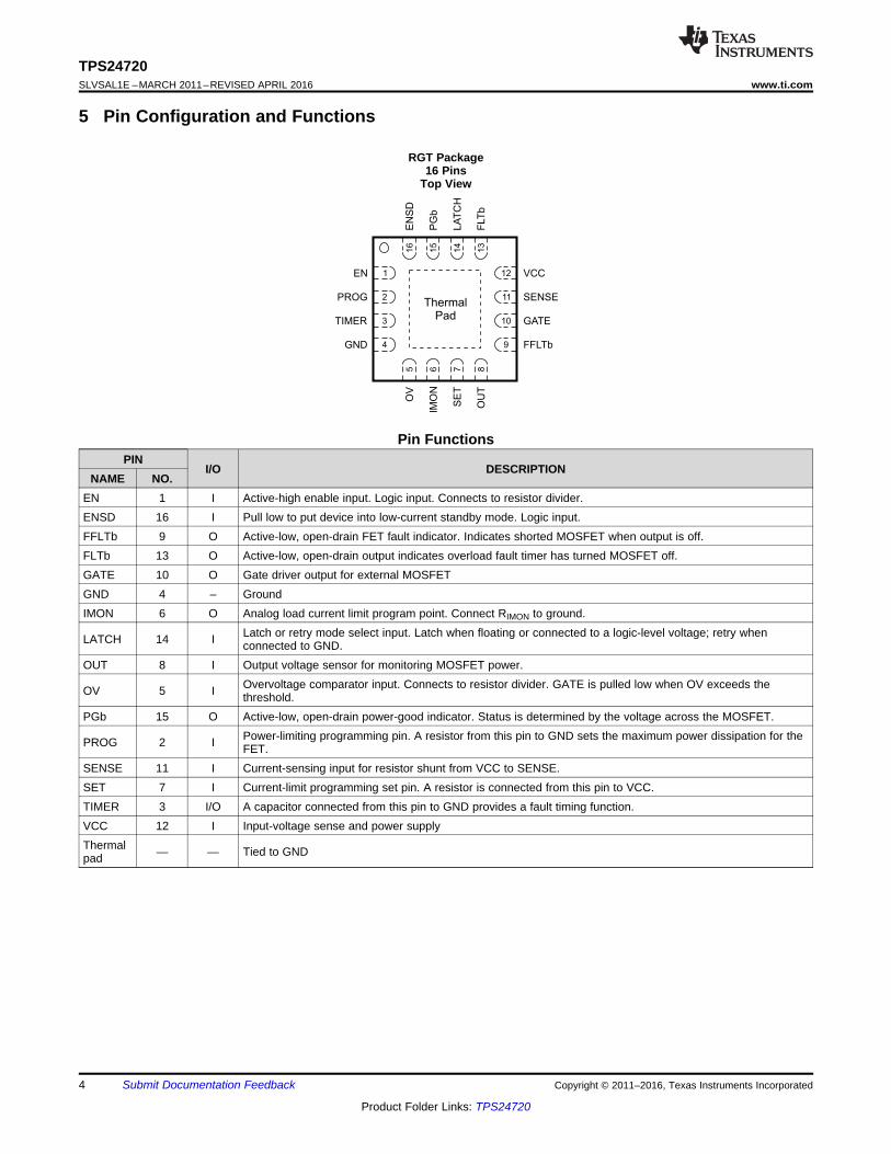
5 Pin Configuration and Functions
RGT Package16 Pins
Top View
Pin FunctionsPIN
I/O DESCRIPTIONNAME NO.
EN 1 I Active-high enable input. Logic input. Connects to resistor divider.ENSD 16 I Pull low to put device into low-current standby mode. Logic input.FFLTb 9 O Active-low, open-drain FET fault indicator. Indicates shorted MOSFET when output is off.FLTb 13 O Active-low, open-drain output indicates overload fault timer has turned MOSFET off.GATE 10 O Gate driver output for external MOSFETGND 4 – GroundIMON 6 O Analog load current limit program point. Connect RIMON to ground.
LATCH 14 I Latch or retry mode select input. Latch when floating or connected to a logic-level voltage; retry whenconnected to GND.
OUT 8 I Output voltage sensor for monitoring MOSFET power.
OV 5 I Overvoltage comparator input. Connects to resistor divider. GATE is pulled low when OV exceeds thethreshold.
PGb 15 O Active-low, open-drain power-good indicator. Status is determined by the voltage across the MOSFET.
PROG 2 I Power-limiting programming pin. A resistor from this pin to GND sets the maximum power dissipation for theFET.
SENSE 11 I Current-sensing input for resistor shunt from VCC to SENSE.SET 7 I Current-limit programming set pin. A resistor is connected from this pin to VCC.TIMER 3 I/O A capacitor connected from this pin to GND provides a fault timing function.VCC 12 I Input-voltage sense and power supplyThermalpad — — Tied to GND
5
TPS24720www.ti.com SLVSAL1E –MARCH 2011–REVISED APRIL 2016
Product Folder Links: TPS24720
Submit Documentation FeedbackCopyright © 2011–2016, Texas Instruments Incorporated
(1) Do not apply voltage directly to these pins.
6 Specifications
6.1 Absolute Maximum Ratingsover operating free-air temperature range, all voltages referred to GND (unless otherwise noted)
MIN MAX UNIT
Input voltage range
EN, FFLTb (1), FLTb(1), GATE, OUT, PGb (1), SENSE, SET (1), VCC –0.3 30
VENSD, OV –0.3 20PROG (1) –0.3 3.6[SET, SENSE] to VCC –0.3 0.3IMON, LATCH, TIMER –0.3 5
Sink current FFLTb, FLTb, PGb 5 mA
Source currentPROG Internally limitedIMON 5 mA
Temperature Maximum junction, TJ Internally limited °C
(1) JEDEC document JEP155 states that 500-V HBM allows safe manufacturing with a standard ESD control process.(2) JEDEC document JEP157 states that 250-V CDM allows safe manufacturing with a standard ESD control process.
6.2 ESD RatingsVALUE UNIT
V(ESD)Electrostaticdischarge
Human-body model (HBM), per ANSI/ESDA/JEDEC JS-001 (1)
All pins except PGb ±2000 VPIN PGb ±500 V
Charged-device model (CDM), per JEDEC specification JESD22-C101 (2) ±500 V
(1) For more information about traditional and new thermal metrics, see the Semiconductor and IC Package Thermal Metrics applicationreport (SPRA953).
6.3 THERMAL INFORMATION
THERMAL METRIC (1) TPS24720UNIT
QFN (16) PINSRθJA Junction-to-ambient thermal resistance 47.3 °C/WRθJCtop Junction-to-case (top) thermal resistance 63.8 °C/WRθJB Junction-to-board thermal resistance 20.9 °C/WψJT Junction-to-top characterization parameter 1.6 °C/WψJB Junction-to-board characterization parameter 21 °C/WRθJCbot Junction-to-case (bottom) thermal resistance 5.1 °C/W
(1) Do not apply voltage directly to these pins.
6.4 Recommended Operating Conditionsover operating free-air temperature range (unless otherwise noted)
MIN NOM MAX UNIT
Input voltage rangeENSD, OV 0 16
VSENSE, SET (1), VCC 2.5 18EN, FFLTb, FLTb, PGb, OUT 0 18
Sink current FFLTb, FLTb, PGb 0 2 mASource current IMON 0 1 mAResistance PROG 4.99 500 kΩExternal capacitance TIMER 1 nFOperating junction temperature range, TJ –40 125 °C
6
TPS24720SLVSAL1E –MARCH 2011–REVISED APRIL 2016 www.ti.com
Product Folder Links: TPS24720
Submit Documentation Feedback Copyright © 2011–2016, Texas Instruments Incorporated
(1) Parameters are provided for reference only, and do not constitute part of TI’s published specifications for purposes of TI productwarranty.
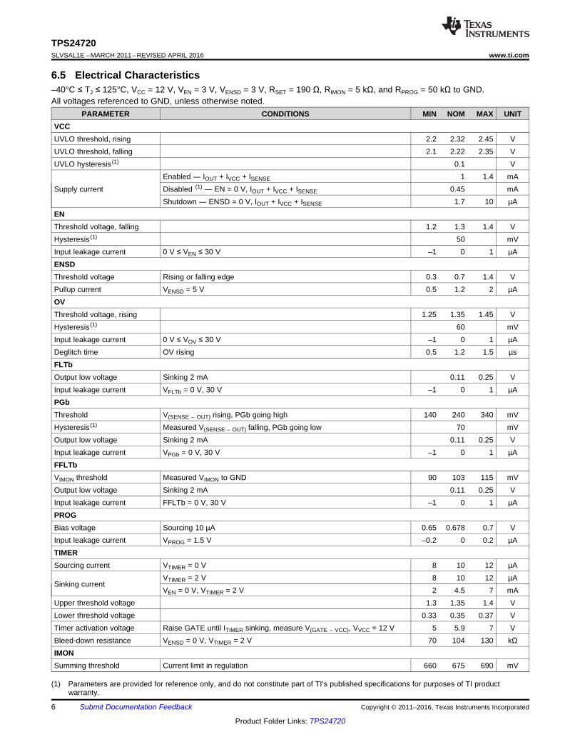
6.5 Electrical Characteristics–40°C ≤ TJ ≤ 125°C, VCC = 12 V, VEN = 3 V, VENSD = 3 V, RSET = 190 Ω, RIMON = 5 kΩ, and RPROG = 50 kΩ to GND.All voltages referenced to GND, unless otherwise noted.
PARAMETER CONDITIONS MIN NOM MAX UNITVCCUVLO threshold, rising 2.2 2.32 2.45 VUVLO threshold, falling 2.1 2.22 2.35 VUVLO hysteresis (1) 0.1 V
Supply currentEnabled ― IOUT + IVCC + ISENSE 1 1.4 mADisabled (1) ― EN = 0 V, IOUT + IVCC + ISENSE 0.45 mAShutdown ― ENSD = 0 V, IOUT + IVCC + ISENSE 1.7 10 µA
ENThreshold voltage, falling 1.2 1.3 1.4 VHysteresis (1) 50 mVInput leakage current 0 V ≤ VEN ≤ 30 V –1 0 1 µAENSDThreshold voltage Rising or falling edge 0.3 0.7 1.4 VPullup current VENSD = 5 V 0.5 1.2 2 µAOVThreshold voltage, rising 1.25 1.35 1.45 VHysteresis (1) 60 mVInput leakage current 0 V ≤ VOV ≤ 30 V –1 0 1 µADeglitch time OV rising 0.5 1.2 1.5 µsFLTbOutput low voltage Sinking 2 mA 0.11 0.25 VInput leakage current VFLTb = 0 V, 30 V –1 0 1 µAPGbThreshold V(SENSE – OUT) rising, PGb going high 140 240 340 mVHysteresis (1) Measured V(SENSE – OUT) falling, PGb going low 70 mVOutput low voltage Sinking 2 mA 0.11 0.25 VInput leakage current VPGb = 0 V, 30 V –1 0 1 µAFFLTbVIMON threshold Measured VIMON to GND 90 103 115 mVOutput low voltage Sinking 2 mA 0.11 0.25 VInput leakage current FFLTb = 0 V, 30 V –1 0 1 µAPROGBias voltage Sourcing 10 µA 0.65 0.678 0.7 VInput leakage current VPROG = 1.5 V –0.2 0 0.2 µATIMERSourcing current VTIMER = 0 V 8 10 12 µA
Sinking currentVTIMER = 2 V 8 10 12 µAVEN = 0 V, VTIMER = 2 V 2 4.5 7 mA
Upper threshold voltage 1.3 1.35 1.4 VLower threshold voltage 0.33 0.35 0.37 VTimer activation voltage Raise GATE until ITIMER sinking, measure V(GATE – VCC), VVCC = 12 V 5 5.9 7 VBleed-down resistance VENSD = 0 V, VTIMER = 2 V 70 104 130 kΩIMONSumming threshold Current limit in regulation 660 675 690 mV
7
TPS24720www.ti.com SLVSAL1E –MARCH 2011–REVISED APRIL 2016
Product Folder Links: TPS24720
Submit Documentation FeedbackCopyright © 2011–2016, Texas Instruments Incorporated
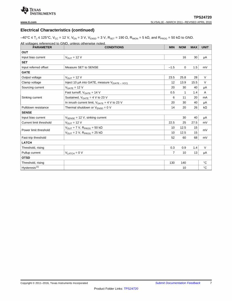
Electrical Characteristics (continued)–40°C ≤ TJ ≤ 125°C, VCC = 12 V, VEN = 3 V, VENSD = 3 V, RSET = 190 Ω, RIMON = 5 kΩ, and RPROG = 50 kΩ to GND.
All voltages referenced to GND, unless otherwise noted.PARAMETER CONDITIONS MIN NOM MAX UNIT
OUTInput bias current VOUT = 12 V 16 30 µASETInput referred offset Measure SET to SENSE –1.5 0 1.5 mVGATEOutput voltage VOUT = 12 V 23.5 25.8 28 VClamp voltage Inject 10 µA into GATE, measure V(GATE – VCC) 12 13.9 15.5 VSourcing current VGATE = 12 V 20 30 40 µA
Sinking currentFast turnoff, VGATE = 14 V 0.5 1 1.4 ASustained, VGATE = 4 V to 23 V 6 11 20 mAIn inrush current limit, VGATE = 4 V to 23 V 20 30 40 µA
Pulldown resistance Thermal shutdown or VENSD = 0 V 14 20 26 kΩSENSEInput bias current VSENSE = 12 V, sinking current 30 40 µACurrent limit threshold VOUT = 12 V 22.5 25 27.5 mV
Power limit thresholdVOUT = 7 V, RPROG = 50 kΩ 10 12.5 15
mVVOUT = 2 V, RPROG = 25 kΩ 10 12.5 15
Fast-trip threshold 52 60 68 mVLATCHThreshold, rising 0.3 0.9 1.4 VPullup current VLATCH = 0 V 7 10 13 µAOTSDThreshold, rising 130 140 °CHysteresis (1) 10 °C

Time
T0494-01
50%
50%
IGATE
VVCC
t(prr50-50)
0
50%
Time
T0495-01
50%
VGATE
VVCC SENSEV–
t(prf50-50)
0
90%
t(pff50-90)
Time
T0492-01
50%
0
VGATE
VEN
t(pff50-90)
Time
T0493-01
50%
VGATE
VENSD
90%
0
8
TPS24720SLVSAL1E –MARCH 2011–REVISED APRIL 2016 www.ti.com
Product Folder Links: TPS24720
Submit Documentation Feedback Copyright © 2011–2016, Texas Instruments Incorporated
(1) Parameters are provided for reference only, and do not constitute part of TI’s published specifications for purposes of TI productwarranty.
6.6 Timing RequirementsMIN NOM MAX UNIT
ENTurnoff time EN ↓ to VGATE < 1 V, CGATE = 33 nF 20 60 150 µsDeglitch time EN ↑ 8 14 18 µs
Disable delay EN ↓ to GATE ↓, CGATE = 0, tpff50–90, SeeFigure 1 0.1 0.4 1 µs
ENSDDisable delay ENSD to GATE, tpff50–90, See Figure 1 0.75 1 µsFFLTbDelay FFLTb falling 60 115 140 msPG, PGbDelay (deglitch) time Rising or falling edge 2 3.4 6 msGATE
Turn on delay VVCC rising to GATE sourcing, tprr50-50, SeeFigure 3 100 250 µs
SENSEFast-turnoff duration 8 13.5 18 µs
Fast-turnoff delay (1) V(VCC – SENSE) = 80 mV, CGATE = 0 pF,tprf50–50, See Figure 4 200 ns
Figure 1. tpff50–90 Timing Definition Figure 2. tpff50–90 Timing Definition
Figure 3. tprr50–50 Timing Definition Figure 4. tprf50–50 Timing Definition

Voltage, V (mV)(VCC )SENSE
40
32
24
16
8
0
8
16
24
32
40
0 5 10 15 20 25 30 35 40 45 50 55
MO
SF
ET
Gate
Curr
ent
(A
)µ
T = 25°C
T = 125°C
Gate Current at Current Limiting
V Voltage = 12 V VCC
T = 40°C Voltage,
V (
V)
()
VC
C
SE
NS
E
10 0 10 20 30 400.2
0
0.2
0.4
0.6
0.8
1
1.2
1.4
1.6
1.8
0.25
0.2
0.15
0.1
0.05
0
0.05
0.1
0.15
0.2
0.25
Time (µs)
Gate
Curr
ent
(A)
V ( )VCC SENSE
T = 125°C
T = 40°C
T = 25°C
V = 12 V VCC
Voltage ,
V (
mV
)(V
CC
S
EN
SE
)
Voltage, V (V)(SENSE OUT)
4
8
12
16
20
24
28
32
0 2 4 6 8 10 12 14
VCC Voltage = 12 V
T = 25°C T = 125°C
T = 40°C
23.5
24
24.5
25
25.5
26
26.5
50 20 10 40 70 100 130
Temperature (°C)
Voltage,
V (
V)
(VC
C
SE
NS
E)
V = 2.5 V VCC
V = 12 V VCC
V = 18 V VCC
400
600
800
1000
1200
0 2 4 6 8 10 12 14 16 18 20Input Voltage, V (V)VCC
Supply
Curr
ent
(µA
) T = 25°C
T = 125°C
T = 40°C
0 2 4 6 8 10 12 14 16 18 20Input Voltage, V (V)VCC
0
1
2
3
4
5
Supply
Curr
ent
(A
)µ
T = 25°C
T = 125°C
T = 40°C
9
TPS24720www.ti.com SLVSAL1E –MARCH 2011–REVISED APRIL 2016
Product Folder Links: TPS24720
Submit Documentation FeedbackCopyright © 2011–2016, Texas Instruments Incorporated
6.7 Typical Characteristics
Figure 5. Supply Current vs Input Voltage at NormalOperation (EN = High)
Figure 6. Supply Current vs Input Voltage at Shutdown(EN = 0 V)
Figure 7. Voltage Across RSENSE in Inrush Current Limitingvs Temperature
Figure 8. Voltage Across RSENSE in Inrush Power Limitingvs VDS of Pass MOSFET
Figure 9. MOSFET Gate Current vs Voltage Across RSENSEDuring Inrush Power Limiting
Figure 10. Gate Current During Fast Trip,VVCC = VGATE = 12 V

UV
LO
Thre
shold
Voltage (
V)
50 20 10 40 70 100 130
Temperature (°C)
V = 12 V VCC
2.20
2.24
2.28
2.32
2.36
UVLO Upper Threshold
UVLO Lower Threshold
0
0.4
0.8
1.2
1.6
2
EN
and E
NS
D T
hre
shold
Voltage (
V)
50 20 10 10 30 50 70 90 110 130
Temperature (°C)
V = 12 V VCC
EN Upper Threshold
ENSD Threshold
TIM
ER
Activation V
oltage T
hre
shold
(V
)
3
4
5
6
7
0 4 8 12 16 20Input Voltage, V (V)VCC
T = 25°C T = 125°C
T = 40°C
0
0.4
0.8
1.2
1.6
2
Fault-T
imer
Period (
ms)
50 20 10 40 70 100 130
Temperature (°C)
V = 12 V VCC C = 10 nF T
C = 4.7 nF T
C = 1 nF T
Gate
Voltage R
efe
renced t
o G
ND
, V
(V
)G
AT
E
0 4 8 12 16 20Input Voltage, V (V)VCC
8
12
16
20
24
28
32
T = 25°C
T = 125°C
T = 40°C
Voltage,
V (
V)
()
VC
C
SE
NS
E
10 0 10 20 30 400.2
0.1
0
0.1
0.2
0.3
0.4
0.5
0.6
0.7
0.9
0.25
0.2
0.15
0.1
0.05
0
0.05
0.1
0.15
0.2
0.25
Time (µs)
Gate
Curr
ent
(A)
V = 3.3 V VCC
V ( )VCC SENSE
T = 125°C
T = 40°C
T = 25°C
10
TPS24720SLVSAL1E –MARCH 2011–REVISED APRIL 2016 www.ti.com
Product Folder Links: TPS24720
Submit Documentation Feedback Copyright © 2011–2016, Texas Instruments Incorporated
Typical Characteristics (continued)
Figure 11. Gate Current During Fast Trip,VVCC = VGATE = 3.3 V Figure 12. Gate Voltage With Zero Gate Current
vs Input Voltage
Figure 13. TIMER Activation Voltage Thresholdvs Input Voltage at Various Temperatures
Figure 14. Fault-Timer vs Temperature With VariousTIMER Capacitors
Figure 15. EN and ENSD Threshold Voltage vs Temperature Figure 16. UVLO Threshold Voltage vs Temperature

0 4 8 12 16 20Input Voltage, V (V)VCC
0.2
0.3
0.4
0.5
0.6
0.7
Supply
Curr
ent
(A
)µ
V = 0 V EN
T = 25°C
T = 125°C
T = 40°C
Low
-Sta
te O
pen-D
rain
Outp
ut
Voltage (
mV
)
60
80
100
120
140
160
50 20 10 40 70 100 130
Temperature (°C)
V = 2.5 V VCC
V = 12 V VCC
V = 18 V VCC
Low
-Sta
te O
pen-D
rain
Outp
ut
Voltage (
mV
)
60
80
100
120
140
160
50 20 10 40 70 100 130
Temperature (°C)
V = 2.5 V VCC
V = 12 V VCC
V = 18 V VCC
Low
-Sta
te O
pen-D
rain
Outp
ut
Voltage (
mV
)
60
80
100
120
140
160
50 20 10 40 70 100 130
Temperature (°C)
V = 2.5 V VCC
V = 12 V VCC
V = 18 V VCC
60
Fast-
Trip T
hre
shold
Voltage (
mV
)
50 20 10 40 70 100 130
Temperature (°C)
60.5
61
61.5
62
62.5
63
63.5
64
V = 2.5 V VCC
V = 12 V VCC
V = 18 V VCC
140
160
180
200
220
240
Vm
V)
(SE
NS
EO
UT
)–
Thre
shold
Voltage (
–50 –20 10 40 70 100 130
Temperature (°C)
PGb Falling
PGb Rising
11
TPS24720www.ti.com SLVSAL1E –MARCH 2011–REVISED APRIL 2016
Product Folder Links: TPS24720
Submit Documentation FeedbackCopyright © 2011–2016, Texas Instruments Incorporated
Typical Characteristics (continued)
Figure 17. Threshold Voltage of VDS vs Temperature,PGb Rising and Falling
Figure 18. Fast-Trip Threshold Voltage vs Temperature
Figure 19. PGb Open-Drain Output Voltage in Low State Figure 20. FLTb Open-Drain Output Voltage in Low State
Figure 21. FFLTb Open-Drain Output Voltage in Low State Figure 22. Supply Current vs Input Voltage at VariousTemperatures When EN Pulled Low

OV,
LA
TC
H T
hre
shold
Voltage (
V)
0.8
1
1.2
1.4
1.6
50 20 10 40 70 100 130
Temperature (°C)
OV Upper Threshold
Latch Threshold
9.5
9.6
9.7
9.8
9.9
10
10.1
10.2
Tim
er
Sourc
ing C
urr
ent
(A
)µ
50 20 10 40 70 100 130
Temperature (°C)
V = 2.5 V VCC
V = 12 V VCC
V = 18 V VCC
9.7
9.8
9.9
10
10.1
10.2
10.3
10.4
Tim
er
Curr
ent
(A
)S
inkin
gµ
50 20 10 40 70 100 130
Temperature (°C)
V = 2.5 V VCC
V = 12 V VCC
V = 18 V VCC
1.334
1.336
1.338
1.34
1.342
1.344
Tim
er
Upper
Thre
shold
Voltage (
V)
50 20 10 40 70 100 130
Temperature (°C)
V = 2.5 V VCC
V = 12 V VCC
V = 18 V VCC
Tim
er
Low
er
Thre
shold
Voltage (
V)
0.357
0.36
0.362
0.365
50 20 10 40 70 100 130
Temperature (°C)
V = 2.5 V VCC
V = 12 V VCC
V = 18 V VCC
12
TPS24720SLVSAL1E –MARCH 2011–REVISED APRIL 2016 www.ti.com
Product Folder Links: TPS24720
Submit Documentation Feedback Copyright © 2011–2016, Texas Instruments Incorporated
Typical Characteristics (continued)
Figure 23. Timer Upper Threshold Voltage vs Temperatureat Various Input Voltages
Figure 24. Timer Lower Threshold Voltage vs Temperatureat Various Input Voltages
Figure 25. Timer Sourcing Current vs Temperature atVarious Input Voltages
Figure 26. Timer Sinking Current vs Temperature at VariousInput Voltages
Figure 27. OV and LATCH Threshold Voltage vs Temperature
0.7 V
POR
Turn Off Main Circuit
ENSD
10 μA
0.9 V
+
+
+VCC
GATE
0~60 µA
11 mA
30 µA+
60 mV
1-shot
2.22 V
UVLO
1.5 V
Fault Logic
1.35 V
0.35 V
ChargePump
SENSESETRGATE
RSET
PROG
IMON
2.32 V
OUT
VIN
–
ServoAmplifier Fast
Comparator
OUT PGb
FLTb
14 µs
TSD
DC
PGComparator
Main Opamp in InrushBecomes Comparator
After Inrush LimitComplete
2 ms
10 µA
10 µA
+
+
–
VCC
5.9 V
GateComparator
20 kΩ
TIMER
InrushLatch
240 mV
+
GND
M1
CT
DC
S
R
Q
Q
+
170 mV
+
+
RSENSE
RPROG
RIMON
++
1.3 V
1.35 V
+
1EN
2
6
12
3
8
15
13
4
11
–
–
–
–
–
–
–
–
10
1.2 μs5OV
+1.29 V1.35 V
16
FFLTb9
7
LATCH
14
A
B
KpA, 675 mV
BMin
æ öç ÷è ø
Copyright © 2016, Texas Instruments Incorporated
13
TPS24720www.ti.com SLVSAL1E –MARCH 2011–REVISED APRIL 2016
Product Folder Links: TPS24720
Submit Documentation FeedbackCopyright © 2011–2016, Texas Instruments Incorporated
7 Detailed Description
7.1 Overview
7.2 Functional Block Diagram
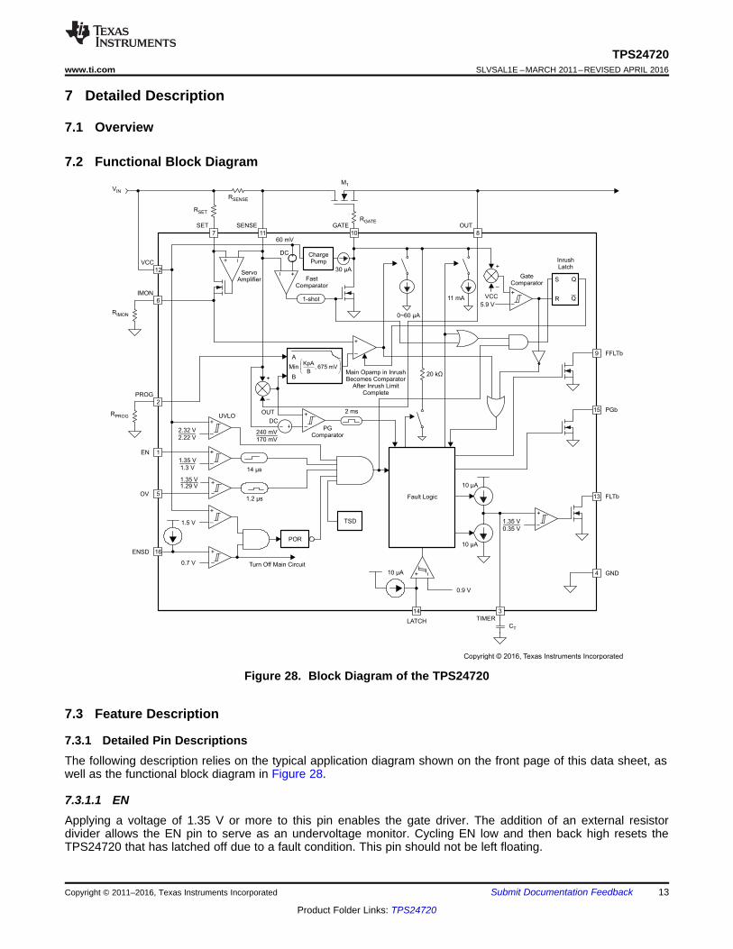
Figure 28. Block Diagram of the TPS24720
7.3 Feature Description
7.3.1 Detailed Pin DescriptionsThe following description relies on the typical application diagram shown on the front page of this data sheet, aswell as the functional block diagram in Figure 28.
7.3.1.1 ENApplying a voltage of 1.35 V or more to this pin enables the gate driver. The addition of an external resistordivider allows the EN pin to serve as an undervoltage monitor. Cycling EN low and then back high resets theTPS24720 that has latched off due to a fault condition. This pin should not be left floating.
14
TPS24720SLVSAL1E –MARCH 2011–REVISED APRIL 2016 www.ti.com
Product Folder Links: TPS24720
Submit Documentation Feedback Copyright © 2011–2016, Texas Instruments Incorporated
Feature Description (continued)7.3.1.2 ENSDWhen this pin is pulled low, it shuts off all internal circuitry and thus places the device in a low-current standbymode. While in standby, the PGb, FLTb, and FFLTb outputs assume high-impedance states. A 20-kΩ resistorpulls GATE to GND in standby. This is a much weaker pulldown than the 11 mA drawn while the part is disabled(e.g., by EN, UVLO, OV, or overload fault current). Applications requiring rapid turnoff should disable the deviceusing the EN pin before pulling ENSD low. This pin is preferably pulled up to a positive voltage from 2 V to 18 V,if not otherwise connected.
7.3.1.3 FFLTbThis active-low open-drain output pulls low if VVCC is higher than the UVLO rising threshold and the voltage onthe IMON pin exceeds 103 mV when EN is disabled. The presence of this voltage indicates that currentcontinues to flow through the external circuitry even though the external MOSFET has been turned off. Thispresumably indicates a shorted MOSFET. FFLTb assumes a high impedance if one of the following conditionsoccurs:• ENSD is pulled low.• Temperature on the die exceeds the OTSD shutdown threshold.• VVCC drops below the UVLO falling threshold.
FFLTb also asserts if VVCC is higher than the UVLO rising threshold, GATE is disabled by OV, and the voltage onthe IMON pin exceeds 103 mV. This pin can be left floating when not used.
7.3.1.4 FLTbThis active-low open-drain output pulls low when the TPS24720 has remained in current limit long enough for thefault timer to expire. The behavior of the FLTb pin depends on the status of the LATCH pin. If the LATCH pin isheld high or left floating, the TPS24720 operates in latch mode. If the LATCH pin is held low, the TPS24720operates in retry mode. In latch mode, a fault timeout disables the external MOSFET and holds FLTb low. Thelatched mode of operation is reset by cycling EN, VCC, or ENSD. In retry mode, a fault timeout first disables theexternal MOSFET, next waits sixteen cycles of TIMER charging and discharging, and finally attempts a restart.This process repeats as long as the fault persists. In retry mode, the FLTb pin is pulled low whenever theexternal MOSFET is disabled by the fault timer. In a sustained fault, the FLTb waveform becomes a train ofpulses. The FLTb pin does not assert if the external MOSFET is disabled by EN, ENSD, OV, overtemperatureshutdown, or UVLO. This pin can be left floating when not used.
7.3.1.5 GATEThis pin provides gate drive to the external MOSFET. A charge pump sources 30 µA to enhance the externalMOSFET. A 13.9-V clamp between GATE and VCC limits the gate-to-source voltage, because VVCC is very closeto VOUT in normal operation. During start-up, a transconductance amplifier regulates the gate voltage of M1 toprovide inrush current limiting. The TIMER pin charges timer capacitor CT during the inrush. Inrush currentlimiting continues until the V(GATE – VCC) exceeds the Timer Activation Voltage (5.9 V for VVCC = 12 V). Then theTPS24720 enters into circuit-breaker mode. The Timer Activation Voltage is defined as a threshold voltage.When V(GATE-VCC) exceeds this threshold voltage, the inrush operation is finished and the TIMER stops sourcingcurrent and begins sinking current. In the circuit-breaker mode, the current flowing in RSENSE is compared withthe current-limit threshold derived from the MOSFET power-limit scheme (see PROG). If the current flowing inRSENSE exceeds the current limit threshold, then MOSFET M1 is turned off. The GATE pin is disabled by thefollowing three mechanisms:1. GATE is pulled down by an 11-mA current source when
– The fault timer expires during an overload current fault (VIMON > 675 mV)– VEN is below its falling threshold– VVCC drops below the UVLO threshold– VOV is above its rising threshold
2. GATE is pulled down by a 1-A current source for 13.5 µs when a hard output short circuit occurs and V(VCC –SENSE) is greater than 60 mV, i.e., the fast-trip shutdown threshold. After fast-trip shutdown is complete, an11-mA sustaining current ensures that the external MOSFET remains off.
3. GATE is discharged by a 20-kΩ resistor to GND if the chip die temperature exceeds the OTSD rising
15
TPS24720www.ti.com SLVSAL1E –MARCH 2011–REVISED APRIL 2016
Product Folder Links: TPS24720
Submit Documentation FeedbackCopyright © 2011–2016, Texas Instruments Incorporated
Feature Description (continued)threshold or ENSD is pulled low.
GATE remains low in latch mode and attempts a restart periodically in retry mode.
No external resistor should be directly connected from GATE to GND or from GATE to OUT.
7.3.1.6 GNDThis pin is connected to system ground.
7.3.1.7 IMONA resistor connected from this pin to GND scales the current-limit and power-limit settings, as illustrated inFigure 28. The voltage present at this pin is proportional to the current flowing through sense resistor RSENSE.This voltage can be used as a means of monitoring current flow through the system. The value of RIMON can becalculated from Equation 3. This pin should not have a bypass capacitor or any other load except for RIMON.
7.3.1.8 LATCHThis pin determines whether the TPS24720 operates in latch mode or retry mode. Applying a voltage of 2 V to 5V to this pin or allowing it to float selects latch mode. Tying the pin to ground selects retry mode. In latch mode,an overload current fault disables the TPS24720 until EN, ENSD, or VCC is cycled. In retry mode, the TPS24720automatically attempts a restart after every sixteen cycles of TIMER charging and discharging. In a sustainedfault in retry mode, the external MOSFET conducts 3.93% of the time; i.e., the duty ratio is 0.0393. If the LATCHpin is allowed to float, then its open-circuit voltage is approximately 2.28 V.
7.3.1.9 OUTThis pin allows the controller to measure the drain-to-source voltage across the external MOSFET M1. Thepower-good indicator (PGb) relies on this information, as does the power-limiting engine. The OUT pin should beprotected from negative voltage transients by a clamping diode or sufficient capacitors. A Schottky diode of 3 A /40 V in a SMC package is recommended as a clamping diode for high-power applications. The OUT pin shouldbe bypassed to GND with a low-impedance ceramic capacitor in the range of 10 nF to 1 µF.
7.3.1.10 OVThis pin is used to program the device overvoltage level. A voltage of more than 1.35 V on this pin turns off theexternal MOSFET. A resistor divider connected from VCC to this pin provides overvoltage protection for thedownstream load. This pin should be tied to GND when not used.
7.3.1.11 PGbThis active-low, open-drain output is intended to interface to downstream dc/dc converters or monitoring circuits.PGb pulls low after the drain-to-source voltage of the FET has fallen below 170 mV and a 3.4-ms deglitch delayhas elapsed. It goes open-drain when VDS exceeds 240 mV. PGb assumes high-impedance status after a 3.4-msdeglitch delay once VDS of M1 rises up, resulting from GATE being pulled to GND at any of the followingconditions:• An overload current fault occurs (VIMON > 675 mV).• A hard output short circuit occurs, leading to V(VCC – SENSE) greater than 60 mV, i.e., the fast-trip shutdown
threshold has been exceeded.• VEN is below its falling threshold.• VENSD is below its threshold.• VVCC drops below the UVLO threshold.• VOV is above its rising threshold.• Die temperature exceeds the OTSD threshold.
This pin can be left floating when not used.

T FLT
10 μAC = t
1.35 V´
SETLIM
IMON SENSE
0.675 V RI =
R R
´
´
J(MAX) C(MAX)LIM
θJC(MAX)
T TP <
R
-
SETLIM
PROG SENSE IMON
R84375P
R R R= ´
´
16
TPS24720SLVSAL1E –MARCH 2011–REVISED APRIL 2016 www.ti.com
Product Folder Links: TPS24720
Submit Documentation Feedback Copyright © 2011–2016, Texas Instruments Incorporated
Feature Description (continued)7.3.1.12 PROGA resistor from this pin to GND sets the maximum power permitted in the external MOSFET M1 during inrush. Donot apply a voltage to this pin. If the constant power limit is not desired, use a PROG resistor of 4.99 kΩ. To setthe maximum power, use Equation 1,
(1)
where PLIM is the allowed power limit of MOSFET M1. RSENSE is the load-current-monitoring resistor connectedbetween the VCC pin and the SENSE pin. RPROG is the resistor connected from the PROG pin to GND. BothRPROG and RSENSE are in ohms and PLIM is in watts. PLIM is determined by the maximum allowed thermal stress ofMOSFET M1, given by Equation 2,
(2)
where TJ(MAX) is the maximum desired transient junction temperature and TC(MAX) is the maximum casetemperature prior to a start or restart. RӨJC(MAX) is the junction-to-case thermal impedance of the pass MOSFETM1 in units of °C/W. Both TJ(MAX) and TC(MAX) are in °C.
7.3.1.13 SENSEThis pin connects to the negative terminal of RSENSE. It provides a means of sensing the voltage across thisresistor, as well as a way to monitor the drain-to-source voltage across the external FET. The current limit ILIM isset by Equation 3.
(3)
A fast-trip shutdown occurs when V(VCC – VSENSE) exceeds 60 mV.
7.3.1.14 SETA resistor RSET is connected from this pin to the positive terminal of RSENSE. This resistor scales the current limitand power limit settings. It coordinates with RIMON and RSENSE to determine the current limit value. The value ofRSET can be calculated from Equation 3 (see SENSE).
7.3.1.15 TIMERA capacitor CT connected from the TIMER pin to GND determines the overload fault timing. TIMER sources 10µA when an overload is present, and discharges CT at 10 µA otherwise. M1 is turned off when VTIMER reaches1.35 V. In an application implementing auto-retry after a fault, this capacitor also determines the period beforethe external MOSFET is re-enabled. A minimum timing capacitance of 1 nF is recommended to ensure properoperation of the fault timer. The value of CT can be calculated from the desired fault time tFLT, using Equation 4.
(4)
As is explained in the description of the LATCH pin, either latch mode or retry mode occurs if the load currentexceeds the current limit threshold or the fast-trip shutdown threshold, depending on the status of the LATCHpin. While in latch mode, the TIMER pin continues to charge and discharge the attached capacitor periodically. Inretry mode, the external MOSFET is disabled for sixteen cycles of TIMER charging and discharging. The TIMERpin is pulled to GND by a 2-mA current source at the end of the 16th cycle of charging and discharging. Theexternal MOSFET is then re-enabled. The TIMER pin capacitor, CT, can also be discharged to GND during latchmode or retry mode in the following two ways:1. A 2-mA current sinks TIMER whenever any of the following occurs:
– VEN is below its falling threshold.– VVCC drops below the UVLO threshold.– VOV is above its rising threshold.
2. A 100-kΩ resistor is connected to TIMER and discharges CT at the moment when VENSD drops below its
17
TPS24720www.ti.com SLVSAL1E –MARCH 2011–REVISED APRIL 2016
Product Folder Links: TPS24720
Submit Documentation FeedbackCopyright © 2011–2016, Texas Instruments Incorporated
Feature Description (continued)threshold.
TIMER is not affected when the die temperature exceeds the OTSD threshold.
7.3.1.16 VCCThis pin performs three functions. First, it provides biasing power to the integrated circuit. Second, it serves as aninput to the power-on reset (POR) and undervoltage lockout (UVLO) functions. The VCC trace from theintegrated circuit should connect directly to the positive terminal of RSENSE to minimize the voltage sensing error.Bypass capacitor C1, shown in the typical application diagram on the front page, should be connected to thepositive terminal of RSENSE. A capacitance of at least 10 nF is recommended.
7.4 Device Functional ModesThe TPS24720 provides all the features needed for a positive hot-swap controller. These features include:• Undervoltage lockout• Adjustable (system-level) enable• Turn-on inrush limiting• High-side gate drive for an external N-channel MOSFET• MOSFET protection by power limiting• Adjustable overload timeout, also called an electronic circuit breaker• Charge-complete indicator for downstream converter coordination• A choice of latch or automatic restart mode• A low-power disable mode accessed by holding ENSD low• MOSFET short detection• Load overvoltage protection
The typical application diagram, shown on the front page of this datasheet, and oscilloscope plots, shown inFigure 29 through Figure 31 and Figure 33 through Figure 36, demonstrate many of the functions describedpreviously.
7.4.1 Board Plug-InFigure 29 and Figure 30 illustrate the inrush current that flows when a hot swap board under the control of theTPS24720 is plugged into a system bus. Only the bypass capacitor charge current and small bias currents areevident when a board is first plugged in. The TPS24720 is held inactive for a short period while internal voltagesstabilize. In this short period, GATE, PROG, and TIMER are held low and PGb, FLTb, and FFLTb are held open-drain. When the voltage on the internal VCC rail exceeds approximately 1.5 V, the power-on reset (POR) circuitinitializes the TPS24720 and a start-up cycle is ready to take place.
GATE, PROG, TIMER, PGb, FLTb and FFTb are released after the internal voltages have stabilized and theexternal EN (enable) thresholds have been exceeded. The part begins sourcing current from the GATE pin toturn on MOSFET M1. The TPS24720 monitors both the drain-to-source voltage across MOSFET M1 and thedrain current passing through it. Based on these measurements, the TPS24720 limits the drain current bycontrolling the gate voltage so that the power dissipation within the MOSFET does not exceed the power limitprogrammed by the user. The current increases as the voltage across the MOSFET decreases until finally thecurrent reaches the current limit ILIM.
18
TPS24720SLVSAL1E –MARCH 2011–REVISED APRIL 2016 www.ti.com
Product Folder Links: TPS24720
Submit Documentation Feedback Copyright © 2011–2016, Texas Instruments Incorporated
Device Functional Modes (continued)
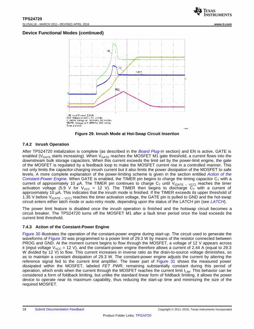
Figure 29. Inrush Mode at Hot-Swap Circuit Insertion
7.4.2 Inrush OperationAfter TPS24720 initialization is complete (as described in the Board Plug-In section) and EN is active, GATE isenabled (VGATE starts increasing). When VGATE reaches the MOSFET M1 gate threshold, a current flows into thedownstream bulk storage capacitors. When this current exceeds the limit set by the power-limit engine, the gateof the MOSFET is regulated by a feedback loop to make the MOSFET current rise in a controlled manner. Thisnot only limits the capacitor-charging inrush current but it also limits the power dissipation of the MOSFET to safelevels. A more complete explanation of the power-limiting scheme is given in the section entitled Action of theConstant-Power Engine. When GATE is enabled, the TIMER pin begins to charge the timing capacitor CT with acurrent of approximately 10 µA. The TIMER pin continues to charge CT until V(GATE – VCC) reaches the timeractivation voltage (5.9 V for VVCC = 12 V). The TIMER then begins to discharge CT with a current ofapproximately 10 µA. This indicates that the inrush mode is finished. If the TIMER exceeds its upper threshold of1.35 V before V(GATE – VCC) reaches the timer activation voltage, the GATE pin is pulled to GND and the hot-swapcircuit enters either latch mode or auto-retry mode, depending upon the status of the LATCH pin (see LATCH).
The power limit feature is disabled once the inrush operation is finished and the hotswap circuit becomes acircuit breaker. The TPS24720 turns off the MOSFET M1 after a fault timer period once the load exceeds thecurrent limit threshold.
7.4.3 Action of the Constant-Power EngineFigure 30 illustrates the operation of the constant-power engine during start-up. The circuit used to generate thewaveforms of Figure 30 was programmed to a power limit of 29.3 W by means of the resistor connected betweenPROG and GND. At the moment current begins to flow through the MOSFET, a voltage of 12 V appears acrossit (input voltage VVCC = 12 V), and the constant-power engine therefore allows a current of 2.44 A (equal to 29.3W divided by 12 V) to flow. This current increases in inverse ratio as the drain-to-source voltage diminishes, soas to maintain a constant dissipation of 29.3 W. The constant-power engine adjusts the current by altering thereference signal fed to the current limit amplifier. The lower part of Figure 31 shows the measured powerdissipated within the MOSFET, labeled FET PWR, remaining substantially constant during this period ofoperation, which ends when the current through the MOSFET reaches the current limit ILIM. This behavior can beconsidered a form of foldback limiting, but unlike the standard linear form of foldback limiting, it allows the powerdevice to operate near its maximum capability, thus reducing the start-up time and minimizing the size of therequired MOSFET.

C002
I_IN: Input Current, 2 A/divGAT: Voltage on GATE Pin, 5 V/divV_DS: Drain-to-Source Voltage of M1, 5 V/divTIMER: Voltage on TIMER Pin, 500 mV/divFET_PWR: Power on M1 (product of V_DS and I_IN), 19 W/divTime: 10 ms/div
19
TPS24720www.ti.com SLVSAL1E –MARCH 2011–REVISED APRIL 2016
Product Folder Links: TPS24720
Submit Documentation FeedbackCopyright © 2011–2016, Texas Instruments Incorporated
Device Functional Modes (continued)
Figure 30. Computation of M1 Power Stress During Startup
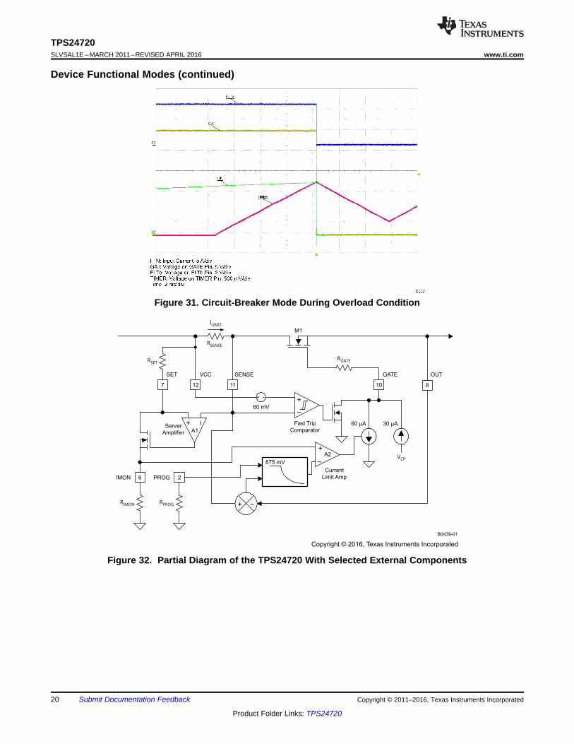
7.4.4 Circuit Breaker and Fast TripThe TPS24720 monitors load current by sensing the voltage across RSENSE. The TPS24720 incorporates twodistinct thresholds: a current-limit threshold and a fast-trip threshold.
The functions of circuit breaker and fast-trip turn off are shown in Figure 31 through Figure 34.
Figure 31 shows the behavior of the TPS24720 when a fault in the output load causes the current passingthrough RSENSE to increase to a value above the current limit but less than the fast-trip threshold. When thecurrent exceeds the current-limit threshold, a current of approximately 10 μA begins to charge timing capacitorCT. If the voltage on CT reaches 1.35 V, then the external MOSFET is turned off. The TPS24720 either latchesoff or commences a restart cycle, depending upon the state of the LATCH pin. In either event, fault pin FLTbpulls low to signal a fault condition. Overload between the current limit and the fast-trip threshold is permitted forthis period. This shutdown scheme is sometimes called an electronic circuit breaker.
The fast-trip threshold protects the system against a severe overload or a dead short circuit. When the voltageacross the sense resistor RSENSE exceeds the 60-mV fast-trip threshold, the GATE pin immediately pulls theexternal MOSFET gate to ground with approximately 1 A of current. This extremely rapid shutdown maygenerate disruptive transients in the system, in which case a low-value resistor inserted between the GATE pinand the MOSFET gate can be used to moderate the turn off current. The fast-trip circuit holds the MOSFET offfor only a few microseconds, after which the TPS24720 turns back on slowly, allowing the current-limit feedbackloop to take over the gate control of M1. Then the hot-swap circuit goes into latch mode or auto-retry mode,depending on pre-determined conditions. Figure 33 and Figure 34 illustrate the behavior of the system when thecurrent exceeds the fast-trip threshold.
OUTGATESET
30 Aμ
60 mV
SENSE
RGATE
PROGIMON
Server
Amplifier
Fast Trip
Comparator
M1
RSENSE
RIMON
RSET
RPROG
B0439-01
ILIMIT
A1
+
+
107 1112
26
+
8
+
–
–
–675 mVV
CP
60 Aμ
A2
VCC
Current
Limit Amp
Copyright © 2016, Texas Instruments Incorporated
20
TPS24720SLVSAL1E –MARCH 2011–REVISED APRIL 2016 www.ti.com
Product Folder Links: TPS24720
Submit Documentation Feedback Copyright © 2011–2016, Texas Instruments Incorporated
Device Functional Modes (continued)
Figure 31. Circuit-Breaker Mode During Overload Condition
Figure 32. Partial Diagram of the TPS24720 With Selected External Components

21
TPS24720www.ti.com SLVSAL1E –MARCH 2011–REVISED APRIL 2016
Product Folder Links: TPS24720
Submit Documentation FeedbackCopyright © 2011–2016, Texas Instruments Incorporated
Device Functional Modes (continued)
Figure 33. Current Limit During Output-Load Short-CircuitCondition (Overview)
Figure 34. Current Limit During Output-Load Short-CircuitCondition (Onset)
7.4.5 Automatic RestartIf LATCH is connected to GND, then the TPS24720 automatically initiates a restart after a fault has caused it toturn off the external MOSFET M1. Internal control circuits use CT to count 16 cycles before re-enabling M1 asshown in Figure 35. This sequence repeats if the fault persists. The timer has a 1 : 1 charge-to-discharge currentratio. For the very first cycle, the TIMER pin starts from 0 V and rises to the upper threshold of 1.35 V andsubsequently falls to 0.35 V before restarting. For the following 16 cycles, 0.35 V is used as the lower threshold.This small duty cycle often reduces the average short-circuit power dissipation to levels associated with normaloperation and eliminates special thermal considerations for surviving a prolonged output short.
Figure 35. Auto-Restart Cycle Timing Figure 36. Latch After Overload Fault
22
TPS24720SLVSAL1E –MARCH 2011–REVISED APRIL 2016 www.ti.com
Product Folder Links: TPS24720
Submit Documentation Feedback Copyright © 2011–2016, Texas Instruments Incorporated
Device Functional Modes (continued)7.4.6 PGb, FLTb, and Timer OperationsThe open-drain PGb output provides a deglitched end-of-inrush indication based on the voltage across M1. PGbis useful for preventing a downstream dc/dc converter from starting while its input capacitor COUT is still charging.PGb goes active-low about 3.4 ms after COUT is charged. This delay allows M1 to fully turn on and any transientsin the power circuits to end before the converter starts up. This type of sequencing prevents the downstreamconverter from demanding full current before the power-limiting engine allows the MOSFET to conduct the fullcurrent set by the current limit ILIM. Failure to observe this precaution may prevent the system from starting. Thepullup resistor shown on the PGb pin in the typical application diagram on the front page is illustrative only; theactual connection to the converter depends on the application. The PGb pin may indicate that inrush has endedbefore the MOSFET is fully enhanced, but the downstream capacitor will have been charged to substantially itsfull operating voltage. Care should be taken to ensure that the MOSFET on-resistance is sufficiently small toensure that the voltage drop across this transistor is less than the minimum power-good threshold of 140 mV.After the hot-swap circuit successfully starts up, the PGb pin can return to a high-impedance status whenever thedrain-to-source voltage of MOSFET M1 exceeds its upper threshold of 340 mV, which presents the downstreamconverters a warning flag. This flag may occur as a result of overload fault, output short fault, input overvoltage,higher die temperature, or the GATE shutdown by UVLO, EN or ENSD.
FLTb is an indicator that the allowed fault-timer period during which the load current can exceed the programmedcurrent limit (but not the fast-trip threshold) expires. The fault timer starts when a current of approximately 10 μAbegins to flow into the external capacitor, CT, and ends when the voltage of CT reaches TIMER upper threshold,i.e., 1.35 V. FLTb pulls low at the end of the fault timer. Otherwise, FLTb assumes a high-impedance state.
The fault-timer state requires an external capacitor CT connected between the TIMER pin and GND pin. Theduration of the fault timer is the charging time of CT from 0 V to its upper threshold of 1.35 V. The fault timerbegins to count under any of the following three conditions:1. In the inrush mode, TIMER begins to source current to the timer capacitor, CT, when MOSFET M1 is
enabled. TIMER begins to sink current from the timer capacitor, CT when V(GATE – VCC) exceeds the timeractivation voltage (see the Inrush Operation section). If V(GATE – VCC) does not reach the timer activationvoltage before TIMER reaches 1.35 V, then the TPS24720 disables the external MOSFET M1. After theMOSFET turns off, the timer goes into either latch mode or retry mode, depending on the LATCH pin status.
2. In an overload fault, TIMER begins to source current to the timer capacitor, CT, when the load currentexceeds the programmed current limits. When the timer capacitor voltage reaches its upper threshold of1.35 V, TIMER begins to sink current from the timer capacitor, CT, and the GATE pin is pulled to ground.After the fault timer period, TIMER may go into latch mode or retry mode, depending on the LATCH pinstatus.
3. In output short-circuit fault, TIMER begins to source current to the timer capacitor, CT, when the load currentexceeds the programmed current limits following a fast-trip shutdown of M1. When the timer capacitor voltagereaches its upper threshold of 1.35 V, TIMER begins to sink current from the timer capacitor, CT, and theGATE pin is pulled to ground. After the fault timer period, TIMER may go into latch mode or retry mode,depending on the LATCH pin status.
If the fault current drops below the programmed current limit within the fault timer period, VTIMER decreases andthe pass MOSFET remains enabled.
The behaviors of TIMER are different in the latch mode and retry mode. If the timer capacitor reaches the upperthreshold of 1.35 V, then:• In latch mode, the TIMER pin continues to charge and discharge the attached capacitor periodically until
TPS24720 is disabled by UVLO, EN, ENSD, or OV, as shown in Figure 36.• In retry mode, TIMER charges and discharges CT between the lower threshold of 0.35 V and the upper
threshold of 1.35 V for sixteen cycles before the TPS24720 attempts to re-start. The TIMER pin is pulled toGND at the end of the 16th cycle of charging and discharging and then ramps from 0 V to 1.35 V for the initialhalf-cycle in which the GATE pin sources current. This periodic pattern is stopped once the overload fault isremoved or the TPS24720 is disabled by UVLO, EN, ENSD, or OV.
23
TPS24720www.ti.com SLVSAL1E –MARCH 2011–REVISED APRIL 2016
Product Folder Links: TPS24720
Submit Documentation FeedbackCopyright © 2011–2016, Texas Instruments Incorporated
Device Functional Modes (continued)7.4.7 Overtemperature ShutdownThe TPS24720 includes a built-in overtemperature shutdown circuit designed to disable the gate driver if the dietemperature exceeds approximately 140°C. An overtemperature condition also causes the FLTb, FFLTb andPGb pins to go to high-impedance states. Normal operation resumes once the die temperature has fallenapproximately 10°C.
7.4.8 Start-Up of Hot-Swap Circuit by VCC or ENThe connection and disconnection between a load and the input power bus are controlled by turning on andturning off the MOSFET, M1.
The TPS24720 has two ways to turn on MOSFET M1:• Increasing VVCC above UVLO upper threshold while EN is already higher than its upper threshold sources
current to the GATE pin. After an inrush period, the TPS24720 fully turns on MOSFET M1.• Increasing EN above its upper threshold while VVCC is already higher than the UVLO upper threshold sources
current to the GATE pin. After an inrush period, the TPS24720 fully turns on MOSFET M1.
The EN pin can be used to start up the TPS24720 at a selected input voltage VVCC.
To isolate the load from the input power bus, the GATE pin sinks current and pulls the gate of MOSFET M1 low.The MOSFET can be disabled by any of the following conditions: UVLO, EN, ENSD, load current above thecurrent-limit threshold, hard short at load, OV, or OTSD. Three separate mechanisms pull down the GATE pin:1. GATE is pulled down by an 11-mA current source when any of the following occurs.
– The fault timer expires during an overload current fault (VIMON > 675 mV).– VEN is below its falling threshold.– VVCC drops below the UVLO threshold.– VOV is above its rising threshold.
2. GATE is pulled down by a 1-A current source for 13.5 μs when a hard output short circuit occurs and V(VCC –SENSE) is greater than 60 mV, i.e., the fast-trip shutdown threshold. After fast-trip shutdown is complete, an11-mA sustaining current ensures that the external MOSFET remains off.
3. GATE is discharged by a 20-kΩ resistor to GND if the chip die temperature exceeds the OTSD risingthreshold or ENSD is pulled low.
7.4.9 Minimization of Power Dissipation at STANDY by ENSDThe ENSD pin enables the use of TPS24720 in applications requiring a low-power standby mode. When this pinis pulled below its threshold voltage, all the internal circuitry is switched off and the GATE pin is discharged toGND through a 20-kΩ resistor. Thus, the MOSFET is disabled and power consumption is kept to a minimum.The correct procedure to go into standby mode is first to shut down the TPS24720 by using the EN pin and thento pull the ENSD pin low.
7.4.10 Fault Detection of MOSFET Short With FFLTbOne of the salient features of the TPS24720 is the detection of short-circuited MOSFETs by the FFLTb pin. TheFFLTb is pulled low to indicate a FET short if all the following conditions occur.• EN is below its threshold voltage.• VVCC is above the UVLO threshold.• VIMON > 103 mV.
The fact that GATE is turned off but current is still flowing through RSENSE indicates a drain-to-source short.

TPS24720
R
2 mSENSE
ΩM
CSD16403Q51
CT
56 nF
VCC
OUTGATESENSE
PGb
PROG TIMERGND
OV
EN
R
2.942
kΩ
R
90.9 k1
Ω
R3
10 kΩ
R5
3.01 kΩ
LATCH
IMON
R4
3.01 kΩ
FLTb
FFLTb
R6
3.01 kΩ
ENSD
SET
RSET
51.1 Ω
RPROG
53.6 kΩ
RIMON
1.43 kΩ
VUVLO
OV
LMT
FAULT
= 10.83 V
V = 14.02 V
I = 12 A
t = 7.56 ms
C1
0.1 Fμ
R7
COUT
470 Fμ
VINVOUT
3 VRGATE
10 Ω
Copyright © 2016, Texas Instruments Incorporated
24
TPS24720SLVSAL1E –MARCH 2011–REVISED APRIL 2016 www.ti.com
Product Folder Links: TPS24720
Submit Documentation Feedback Copyright © 2011–2016, Texas Instruments Incorporated
8 Application and Implementation
NOTEInformation in the following applications sections is not part of the TI componentspecification, and TI does not warrant its accuracy or completeness. TI’s customers areresponsible for determining suitability of components for their purposes. Customers shouldvalidate and test their design implementation to confirm system functionality.
8.1 Application InformationThe TPS24720 is a hotswap used to manage inrush current and provide load fault protection. When designing ahotswap, three key scenarios should be considered:• Start-up• Output of a hotswap is shorted to ground when the hotswap is on. This is often referred to as a hot-short.• Powering-up a board when the output and ground are shorted. This is usually called a start-into-short.
Each of these scenarios place stress on the hotswap MOSFET. Take special care when designing the hotswapcircuit to keep the MOSFET within its SOA. The following design example is provided as a guide. Use theTPS24720 Design Calculator (SLVC563) to assist with the detailed design equation calculations.
8.2 Typical ApplicationThis section provides an application example utilizing power limited start-up and MOSFET SOA protection. Thedesign parameters are listed in the Design Requirements section and represent a more moderate level of faultcurrent. For more stringent current levels, refer to either the TPS24720EVM (SLUU458) (25 A design) or thecalculator tool (SLVC563) (50 A design).
Figure 37. Typical Application (12 V at 10 A)
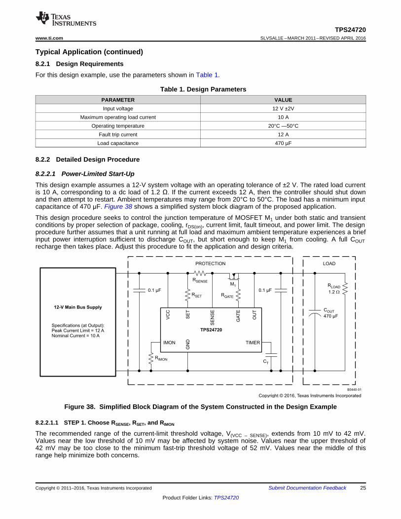
RSET
RIMON
LOADPROTECTION
0.1 Fμ 0.1 Fμ
B0440-01
M1
12-V Main Bus Supply
TIMER
OU
T
GA
TE
VC
C
SE
NS
E
GN
D
TPS24720Specifications (at Output):Peak Current Limit = 12 ANominal Current = 10 A
R
1.2LOAD
W
C
470 FOUT
μ
CT
RSENSE
RGATE
SE
T
IMON
Copyright © 2016, Texas Instruments Incorporated
25
TPS24720www.ti.com SLVSAL1E –MARCH 2011–REVISED APRIL 2016
Product Folder Links: TPS24720
Submit Documentation FeedbackCopyright © 2011–2016, Texas Instruments Incorporated
Typical Application (continued)8.2.1 Design RequirementsFor this design example, use the parameters shown in Table 1.
Table 1. Design ParametersPARAMETER VALUEInput voltage 12 V ±2V
Maximum operating load current 10 AOperating temperature 20°C —50°C
Fault trip current 12 ALoad capacitance 470 µF
8.2.2 Detailed Design Procedure
8.2.2.1 Power-Limited Start-UpThis design example assumes a 12-V system voltage with an operating tolerance of ±2 V. The rated load currentis 10 A, corresponding to a dc load of 1.2 Ω. If the current exceeds 12 A, then the controller should shut downand then attempt to restart. Ambient temperatures may range from 20°C to 50°C. The load has a minimum inputcapacitance of 470 μF. Figure 38 shows a simplified system block diagram of the proposed application.
This design procedure seeks to control the junction temperature of MOSFET M1 under both static and transientconditions by proper selection of package, cooling, rDS(on), current limit, fault timeout, and power limit. The designprocedure further assumes that a unit running at full load and maximum ambient temperature experiences a briefinput power interruption sufficient to discharge COUT, but short enough to keep M1 from cooling. A full COUTrecharge then takes place. Adjust this procedure to fit the application and design criteria.
Figure 38. Simplified Block Diagram of the System Constructed in the Design Example
8.2.2.1.1 STEP 1. Choose RSENSE, RSET, and RIMON
The recommended range of the current-limit threshold voltage, V(VCC – SENSE), extends from 10 mV to 42 mV.Values near the low threshold of 10 mV may be affected by system noise. Values near the upper threshold of42 mV may be too close to the minimum fast-trip threshold voltage of 52 mV. Values near the middle of thisrange help minimize both concerns.

( )
J(MAX) A(MAX)DS(on)(MAX) 2
MAX JA
DS(on)(MAX) 2
T Tr ,
I R
therefore,
150 C 50 Cr 13.6 m
12 A 51 C/ W
q
-=
´
° - °= = W
´ °
SETIMON
LIM SENSE
IMON
0.675 V RR ,
I R
therefore,
0.675 V 51.1R 1437
12 A 2 m
´=
´
´ W= = W
´ W
26
TPS24720SLVSAL1E –MARCH 2011–REVISED APRIL 2016 www.ti.com
Product Folder Links: TPS24720
Submit Documentation Feedback Copyright © 2011–2016, Texas Instruments Incorporated
To achieve high efficiency, the power dissipation in RSENSE must be kept to a minimum. A RSENSE of 2 mΩdevelops a voltage of 24 mV at the specified peak current limit of 12 A, while dissipating only 200 mW at therated 10-A current. This represents a 0.17% power loss.
For best performance, a current of approximately 0.5 mA (referring to the RECOMMENDED OPERATINGCONDITIONS table) should flow into the SET pin and out of the IMON pin when the TPS24720 is in current limit.The voltage across RSET nominally equals the voltage across RSENSE, or 24 mV. Dividing 24 mV by 0.5 mA givesa recommended value of RSET of 48 Ω. A 51.1-Ω, 1% resistor was chosen. Using Equation 3, the value of RIMONmust equal 1437 Ω, or as near as practically possible. A 1.43-kΩ, 1% resistor was chosen.
(5)
8.2.2.1.2 STEP 2. Choose MOSFET M1
The next design step is to select M1. The TPS24720 is designed to use an N-channel MOSFET with a gate-to-source voltage rating of 20 V.
Devices with lower gate-to-source voltage ratings can be used if a Zener diode is connected so as to limit themaximum gate-to-source voltage the transistor sees.
The next factor to consider is the drain-to-source voltage rating, VDS(MAX), of the MOSFET. Although theMOSFET only sees 12 V dc, it may experience much higher transient voltages during extreme conditions, suchas the abrupt shutoff that occurs during a fast trip. A TVS may be required to limit inductive transients under suchconditions. A transistor with a VDS(MAX) rating of at least twice the nominal input power-supply voltage isrecommended regardless of whether a TVS is used or not.
Next select the on-resistance of the transistor, rDS(on). The maximum on-resistance must not generate a voltagegreater then the minimum power-good threshold voltage of 140 mV. Assuming a current limit of 12 A, amaximum rDS(on) of 11.67 mΩ is required. Also consider the effect of rDS(on) on the maximum operatingtemperature TJ(MAX) of the MOSFET. Equation 6 computes the value of rDS(on)(MAX) at a junction temperature ofTJ(MAX). Most manufacturers list rDS(on)(MAX) at 25°C and provide a derating curve from which values at othertemperatures can be derived. Compute the maximum allowable on-resistance, rDS(on)(MAX), using Equation 6.
(6)
Taking these factors into consideration, the TI CSD16403Q5 was selected for this example. This transistor has aVGS(MAX) rating of 16 V, a VDS(MAX) rating of 25 V, and a maximum rDS(on) of 2.8 mΩ at room temperature. Duringnormal circuit operation, the MOSFET can have up to 10 A flowing through it. The power dissipation of theMOSFET equates to 0.24 W and an 9.6°C rise in junction temperature. This is well within the data sheet limits forthe MOSFET. The power dissipated during a fault (e.g., output short) is far larger than the steady-state power.The power handling capability of the MOSFET must be checked during fault conditions.
8.2.2.1.3 STEP 3. Choose Power-Limit Value, PLIM, and RPROG
MOSFET M1 dissipates large amounts of power during inrush. The power limit PLIM of the TPS24720 should beset to prevent the die temperature from exceeding a short-term maximum temperature, TJ(MAX)2. The short-termTJ(MAX)2 could be set as high as 150°C while still leaving ample margin to the usual manufacturer’s rating of175°C. Equation 7 is an expression for calculating PLIM,
ONt =
2OUT VCC(MAX) OUT VCC(MAX)OUT LIM
LIM LIM VCC(MAX)2LIM LIMLIM
C V C VC Pif P I V
2 P I2 I
´ ´´+ - < ´
´´
OUT VCC(MAX)LIM LIM VCC(MAX)
LIM
C Vif P I V
I
´> ´
( )
( )2
ON 2
therefore,
470 μF 12 V470 μF 29.3 W 470 μF 12 Vt 0.614 ms
2 29.3 W 12 A2 12 A
´´ ´= + - =
´´
LIM SENSESNS PL _MIN
IN_MAX
LIM IN_MAXLIM FB
LIM
P R 29.3 W 2 mV 4.19 mV (> 3 mV)
V 14 V
I V 12 A 14 VP 5.73 (< 10)
P 29.3 W
-
-
´ ´ W= = =
´ ´= = =
SET
PROGLIM SENSE IMON
PROG
R84375R
P R R
therefore,
84375 51.1R 51.45 k
29.3 W 0.002 1430
= ´´
W= ´ = W
´ W W
( )
( ) ( )( )
2J(MAX)2 MAX DS(on) CA A(MAX)
LIMJC
2
LIM
T I r R TP 0.8 ,
R
therefore,
130 C 12 A 0.002 51 C / W 1.8 C / W 50 C
P 0.8 29.3 W1.8 C / W
q
q
é ù- ´ ´ +ë û£ ´
é ù° - ´ W ´ ° - ° + °ê úë û£ ´ =°
27
TPS24720www.ti.com SLVSAL1E –MARCH 2011–REVISED APRIL 2016
Product Folder Links: TPS24720
Submit Documentation FeedbackCopyright © 2011–2016, Texas Instruments Incorporated
(7)
where RθJC is the junction-to-case thermal resistance of the MOSFET, rDS(on) is the its resistance at the maximumoperating temperature, and the factor of 0.8 represents the tolerance of the constant-power engine. For anambient temperature of 50°C, the calculated maximum PLIM is 29.3 W. From Equation 1, a 53.6-kΩ, 1% resistoris selected for RPROG (see Equation 8).
(8)
Power limit fold back (PLIM-FB) is the ratio of operating current limit (ILIM) and minimum power limited (regulated)current (when VOUT = 0 V). Degradation of programmed power limit (PLIM) accuracy and start up issues mayoccur if PLIM-FB is too large. Equation 9 calculates VSNS-PL_MIN (minimum sense voltage during power limit) andPLIM-FB. To ensure reliable operation, verify that PLIM-FB < 10 and VSNS,PL,MIN > 3 mV.
(9)
8.2.2.1.4 STEP 4. Choose Output Voltage Rising Time, tON, and Timing Capacitor CT
The maximum output voltage rise time, tON, set by timer capacitor CT must suffice to fully charge the loadcapacitance COUT without triggering the fault circuitry. Equation 10 defines tON for two possible inrush cases.Assuming that only the load capacitance draws current during startup,
(10)

2 3UVTHRESH UV
1 2 3
R RV V
R R R
+
= ´
+ +
3ENTHRESH OV
1 2 3
RV V
R R R= ´
+ +
T FLT
T
10 μAC = t ,
1.35 V
therefore,
10 μAC = 7 ms 52 nF
1.35 V
´
´ =
ISSFLT ON
GATE
FLT
5.9 V Ct t ,
I
therefore,
5.9 V 2040 pFt 0.614 ms 1.22 ms
20 μA
´
= +
´= + =
28
TPS24720SLVSAL1E –MARCH 2011–REVISED APRIL 2016 www.ti.com
Product Folder Links: TPS24720
Submit Documentation Feedback Copyright © 2011–2016, Texas Instruments Incorporated
The next step is to determine the minimum fault-timer period. In Equation 10, the output rise time is tON. This isthe amount of time it takes to charge the output capacitor up to the final output voltage. However, the fault timeruses the difference between the input voltage and the gate voltage to determine if the TPS24720 is still in inrushlimit. The fault timer continues to run until VGS rises 5.9 V (for VVCC = 12 V) above the input voltage. Someadditional time must be added to the charge time to account for this additional gate voltage rise. The minimumfault time can be calculated using Equation 11,
(11)
where CISS is the MOSFET input capacitance and IGATE is the minimum gate sourcing current of TPS24720, or20 μA. Using the example parameters and the CSD16403Q5 data sheet in Equation 11 leads to a minimum faulttime of 1.22 ms. This time is derived considering the tolerances of COUT, CISS, ILIM, PLIM, IGATE, and VVCC(MAX).The fault timer must be set to a value higher than 1.22 ms to avoid turning off during start-up, but lower than anymaximum fault time limit determined by the device SOA curve (see Figure 39) derated for operating junctiontemperature.
For this example, select 7 ms to allow for variation of system parameters such as temperature, load, componenttolerance, and input voltage. The timing capacitor is calculated in Equation 12 as 52 nF. Selecting the next-highest standard value, 56 nF, yields a 7.56-ms fault time.
(12)
8.2.2.1.5 STEP 5. Calculate the Retry-Mode Duty Ratio
In retry mode, the TPS24720 is on for one charging cycle and off for 16 charge/discharge cycles, as can be seenin Figure 35. The first CT charging cycle is from 0 V to 1.35 V, which gives 7.56 ms. The first CT dischargingcycle is from 1.35 V to 0.35 V, which gives 5.6 ms. Therefore, the total time is 7.56 ms + 33 x 5.6 ms = 192.36ms. As a result, the retry mode duty ratio is 7.56 ms/192.36 ms = 3.93%.
8.2.2.1.6 STEP 6. Select R1, R2, and R3 for UV and OV
Next, select the values of the OV and UV resistors, R1, R2, and R3, as shown in the typical application diagramon the front page. From the TPS24720 electrical specifications, VOVTHRESH = 1.35 V and VENTHRESH = 1.35 V. VOVis the overvoltage trip voltage, which in this case is 14 V. VUV is the undervoltage trip voltage, which for thisexample equals 10.8 V.
(13)
(14)
Assume R3 is 1 kΩ and use Equation 13 to solve for (R2 + R3). Use Equation 14 and the (R2 + R3) fromEquation 13 to solve for R2 and finally for R3. From Equation 13, (R2 + R3) = 9370.4 Ω. From Equation 14,R2 = 296 Ω and R1 = 9.074 kΩ. Scaling all three resistors by a factor of ten to use less supply current for thesevoltage references and using standard 1% resistor values gives R1 = 90.9 kΩ, R2 = 2.94 kΩ, and R3 = 10 kΩ.
29
TPS24720www.ti.com SLVSAL1E –MARCH 2011–REVISED APRIL 2016
Product Folder Links: TPS24720
Submit Documentation FeedbackCopyright © 2011–2016, Texas Instruments Incorporated
8.2.2.1.7 STEP 7. Choose RGATE, R4, R5, R6, and C1
In the typical application diagram on the front page, the gate resistor, RGATE, is intended to suppress high-frequency oscillations. A resistor of 10 Ω serves for most applications, but if M1 has a CISS below 200 pF, then 33Ω is recommended. Applications with larger MOSFETs and very short wiring may not require RGATE. R4, R5, andR6 are required only if PGb, FLTb, and FFLTb are used; these resistors serve as pullups for the open-drainoutput drivers. The current sunk by each of these pins should not exceed 2 mA ( referring to the RecommendedOperating Conditions). C1 is a bypass capacitor to help control transient voltages, unit emissions, and localsupply noise while in the disabled state. Where acceptable, a value in the range of 0.001 μF to 0.1 μF isrecommended.
8.2.2.2 Additional Design Considerations
8.2.2.2.1 Use of PGb
Use the PGb pin to control and coordinate a downstream dc/dc converter. If this is not done, then a long timedelay is needed to allow COUT to fully charge before the converter starts. An undesirable latch-up condition canbe created between the TPS24720 output characteristic and the dc/dc converter input characteristic if theconverter starts while COUT is still charging; using the PGb pin is one way to avoid this.
8.2.2.2.2 Output Clamp Diode
Inductive loads on the output may drive the OUT pin below GND when the circuit is unplugged or during acurrent-limit event. The OUT pin ratings can be satisfied by connecting a diode from OUT to GND. The diodeshould be selected to control the negative voltage at the full short-circuit current. Schottky diodes are generallyrecommended for this application.
8.2.2.2.3 Gate Clamp Diode
The TPS24720 has a relatively well-regulated gate voltage of 12 V–15.5 V with a supply voltage VVCC higherthan 4 V. A small clamp Zener from gate to source of M1 is recommended if VGS of M1 is rated below 12 V. Aseries resistance of several hundred ohms or a series silicon diode is recommended to prevent the outputcapacitance from discharging through the gate driver to ground.
8.2.2.2.4 High-Gate-Capacitance Applications
Gate voltage overstress and abnormally large fault-current spikes can be caused by large gate capacitance. Anexternal gate clamp Zener diode is recommended to assist the internal Zener if the total gate capacitance of M1exceeds about 4000 pF.
8.2.2.2.5 Bypass Capacitors
It is a good practice to provide low-impedance ceramic capacitor bypassing of the VCC and OUT pins. Values inthe range of 10 nF to 1 µF are recommended. Some system topologies are insensitive to the values of thesecapacitors; however, some are not and require minimization of the value of the bypass capacitor. Inputcapacitance on a plug-in board may cause a large inrush current as the capacitor charges through the low-impedance power bus when inserted. This stresses the connector contacts and causes a short voltage sag onthe input bus. Small amounts of capacitance (e.g., 10 nF to 0.1 µF) are often tolerable in these systems.
8.2.2.2.6 Output Short-Circuit Measurements
Repeatable short-circuit testing results are difficult to obtain. The many details of source bypassing, input leads,circuit layout and component selection, output shorting method, relative location of the short, and instrumentationall contribute to variation in results. The actual short itself exhibits a certain degree of randomness as itmicroscopically bounces and arcs. Care in configuration and methods must be used to obtain realistic results. Donot expect to see waveforms exactly like those in the data sheet; every setup differs.
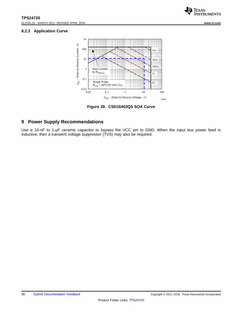
G009
1k
10
0.01
1
100
I
Dra
in-t
o-S
ourc
e C
urr
ent
AD
S0.1
0.01 0.1 10 1001
Single PulseR = 94ºC/W (min Cu)θJA
1ms
10ms
100ms
1s
DC
Area Limitedby RDS(on)
V Drain-to-Source Voltage VDS
30
TPS24720SLVSAL1E –MARCH 2011–REVISED APRIL 2016 www.ti.com
Product Folder Links: TPS24720
Submit Documentation Feedback Copyright © 2011–2016, Texas Instruments Incorporated
8.2.3 Application Curve
Figure 39. CSD16403Q5 SOA Curve
9 Power Supply RecommendationsUse a 10-nF to 1-μF ceramic capacitor to bypass the VCC pin to GND. When the input bus power feed isinductive, then a transient voltage suppressor (TVS) may also be required.
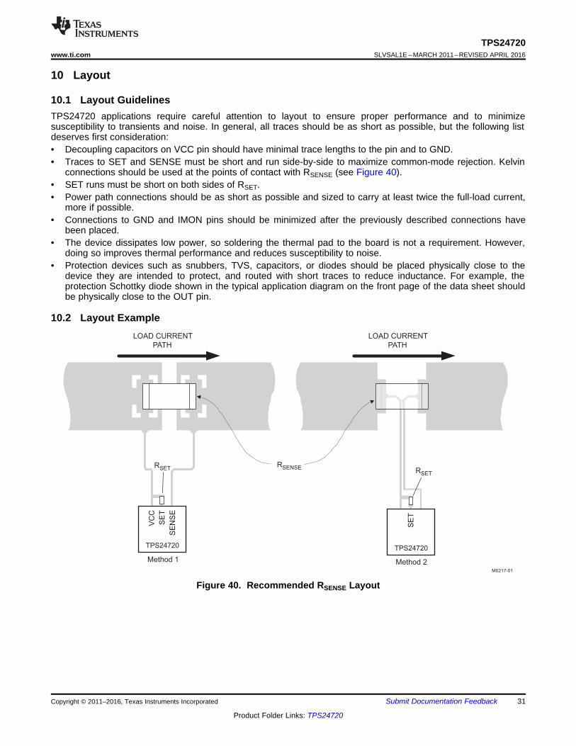
LOAD CURRENT
PATH
RSENSE
LOAD CURRENT
PATH
M0217-01
RSET
RSET
Method 1
SE
NS
E
VC
C
SE
T
TPS24720
Method 2
TPS24720
SE
T
31
TPS24720www.ti.com SLVSAL1E –MARCH 2011–REVISED APRIL 2016
Product Folder Links: TPS24720
Submit Documentation FeedbackCopyright © 2011–2016, Texas Instruments Incorporated
10 Layout
10.1 Layout GuidelinesTPS24720 applications require careful attention to layout to ensure proper performance and to minimizesusceptibility to transients and noise. In general, all traces should be as short as possible, but the following listdeserves first consideration:• Decoupling capacitors on VCC pin should have minimal trace lengths to the pin and to GND.• Traces to SET and SENSE must be short and run side-by-side to maximize common-mode rejection. Kelvin
connections should be used at the points of contact with RSENSE (see Figure 40).• SET runs must be short on both sides of RSET.• Power path connections should be as short as possible and sized to carry at least twice the full-load current,
more if possible.• Connections to GND and IMON pins should be minimized after the previously described connections have
been placed.• The device dissipates low power, so soldering the thermal pad to the board is not a requirement. However,
doing so improves thermal performance and reduces susceptibility to noise.• Protection devices such as snubbers, TVS, capacitors, or diodes should be placed physically close to the
device they are intended to protect, and routed with short traces to reduce inductance. For example, theprotection Schottky diode shown in the typical application diagram on the front page of the data sheet shouldbe physically close to the OUT pin.
10.2 Layout Example
Figure 40. Recommended RSENSE Layout
32
TPS24720SLVSAL1E –MARCH 2011–REVISED APRIL 2016 www.ti.com
Product Folder Links: TPS24720
Submit Documentation Feedback Copyright © 2011–2016, Texas Instruments Incorporated
11 Device and Documentation Support
11.1 Documentation SupportUsing the TPS24720EVM, SLUU458.
TPS24720 Design Calculator, SLVC563
11.2 TrademarksAll trademarks are the property of their respective owners.
11.3 Electrostatic Discharge CautionThese devices have limited built-in ESD protection. The leads should be shorted together or the device placed in conductive foamduring storage or handling to prevent electrostatic damage to the MOS gates.
11.4 GlossarySLYZ022 — TI Glossary.
This glossary lists and explains terms, acronyms, and definitions.
12 Mechanical, Packaging, and Orderable InformationThe following pages include mechanical, packaging, and orderable information. This information is the mostcurrent data available for the designated devices. This data is subject to change without notice and revision ofthis document. For browser-based versions of this data sheet, refer to the left-hand navigation.
PACKAGE OPTION ADDENDUM
www.ti.com 11-Aug-2017
Addendum-Page 1
PACKAGING INFORMATION
Orderable Device Status(1)
Package Type PackageDrawing
Pins PackageQty
Eco Plan(2)
Lead/Ball Finish(6)
MSL Peak Temp(3)
Op Temp (°C) Device Marking(4/5)
Samples
TPS24720RGTR ACTIVE VQFN RGT 16 3000 Green (RoHS& no Sb/Br)
CU NIPDAU Level-2-260C-1 YEAR -40 to 85 24720
TPS24720RGTT ACTIVE VQFN RGT 16 250 Green (RoHS& no Sb/Br)
CU NIPDAU Level-2-260C-1 YEAR -40 to 85 24720
(1) The marketing status values are defined as follows:ACTIVE: Product device recommended for new designs.LIFEBUY: TI has announced that the device will be discontinued, and a lifetime-buy period is in effect.NRND: Not recommended for new designs. Device is in production to support existing customers, but TI does not recommend using this part in a new design.PREVIEW: Device has been announced but is not in production. Samples may or may not be available.OBSOLETE: TI has discontinued the production of the device.
(2) RoHS: TI defines "RoHS" to mean semiconductor products that are compliant with the current EU RoHS requirements for all 10 RoHS substances, including the requirement that RoHS substancedo not exceed 0.1% by weight in homogeneous materials. Where designed to be soldered at high temperatures, "RoHS" products are suitable for use in specified lead-free processes. TI mayreference these types of products as "Pb-Free".RoHS Exempt: TI defines "RoHS Exempt" to mean products that contain lead but are compliant with EU RoHS pursuant to a specific EU RoHS exemption.Green: TI defines "Green" to mean the content of Chlorine (Cl) and Bromine (Br) based flame retardants meet JS709B low halogen requirements of <=1000ppm threshold. Antimony trioxide basedflame retardants must also meet the <=1000ppm threshold requirement.
(3) MSL, Peak Temp. - The Moisture Sensitivity Level rating according to the JEDEC industry standard classifications, and peak solder temperature.
(4) There may be additional marking, which relates to the logo, the lot trace code information, or the environmental category on the device.
(5) Multiple Device Markings will be inside parentheses. Only one Device Marking contained in parentheses and separated by a "~" will appear on a device. If a line is indented then it is a continuationof the previous line and the two combined represent the entire Device Marking for that device.
(6) Lead/Ball Finish - Orderable Devices may have multiple material finish options. Finish options are separated by a vertical ruled line. Lead/Ball Finish values may wrap to two lines if the finishvalue exceeds the maximum column width.
Important Information and Disclaimer:The information provided on this page represents TI's knowledge and belief as of the date that it is provided. TI bases its knowledge and belief on informationprovided by third parties, and makes no representation or warranty as to the accuracy of such information. Efforts are underway to better integrate information from third parties. TI has taken andcontinues to take reasonable steps to provide representative and accurate information but may not have conducted destructive testing or chemical analysis on incoming materials and chemicals.TI and TI suppliers consider certain information to be proprietary, and thus CAS numbers and other limited information may not be available for release.
In no event shall TI's liability arising out of such information exceed the total purchase price of the TI part(s) at issue in this document sold by TI to Customer on an annual basis.
PACKAGE OPTION ADDENDUM
www.ti.com 11-Aug-2017
Addendum-Page 2

TAPE AND REEL INFORMATION
*All dimensions are nominal
Device PackageType
PackageDrawing
Pins SPQ ReelDiameter
(mm)
ReelWidth
W1 (mm)
A0(mm)
B0(mm)
K0(mm)
P1(mm)
W(mm)
Pin1Quadrant
TPS24720RGTR VQFN RGT 16 3000 330.0 12.4 3.3 3.3 1.1 8.0 12.0 Q2
TPS24720RGTR VQFN RGT 16 3000 330.0 12.4 3.3 3.3 1.1 8.0 12.0 Q2
TPS24720RGTT VQFN RGT 16 250 180.0 12.4 3.3 3.3 1.1 8.0 12.0 Q2
TPS24720RGTT VQFN RGT 16 250 180.0 12.5 3.3 3.3 1.1 8.0 12.0 Q2
PACKAGE MATERIALS INFORMATION
www.ti.com 11-Aug-2017
Pack Materials-Page 1
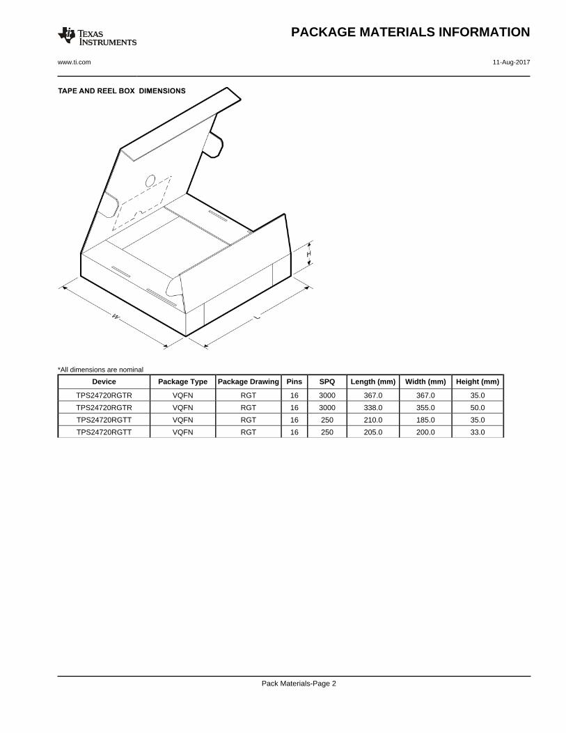
*All dimensions are nominal
Device Package Type Package Drawing Pins SPQ Length (mm) Width (mm) Height (mm)
TPS24720RGTR VQFN RGT 16 3000 367.0 367.0 35.0
TPS24720RGTR VQFN RGT 16 3000 338.0 355.0 50.0
TPS24720RGTT VQFN RGT 16 250 210.0 185.0 35.0
TPS24720RGTT VQFN RGT 16 250 205.0 200.0 33.0
PACKAGE MATERIALS INFORMATION
www.ti.com 11-Aug-2017
Pack Materials-Page 2

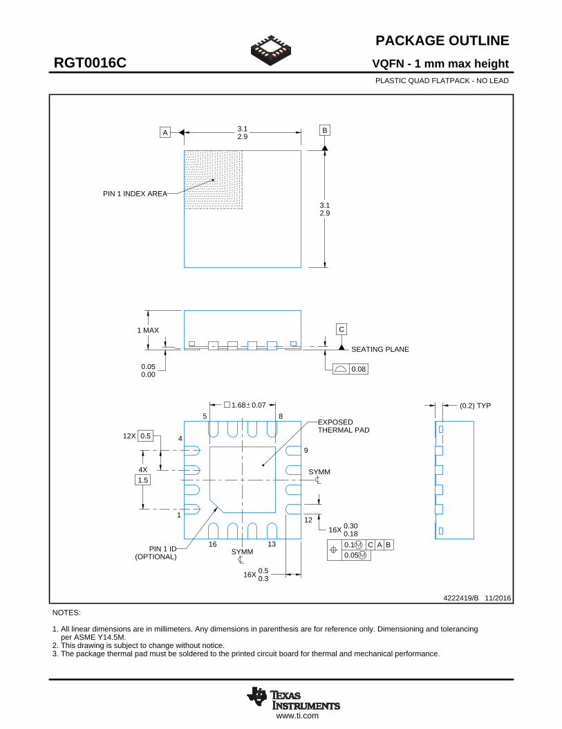
www.ti.com
PACKAGE OUTLINE
C
16X 0.300.18
1.68 0.07
16X 0.50.3
1 MAX
(0.2) TYP
0.050.00
12X 0.5
4X1.5
A 3.12.9
B
3.12.9
VQFN - 1 mm max heightRGT0016CPLASTIC QUAD FLATPACK - NO LEAD
4222419/B 11/2016
PIN 1 INDEX AREA
0.08
SEATING PLANE
1
49
12
5 8
16 13
(OPTIONAL)PIN 1 ID 0.1 C A B
0.05
EXPOSEDTHERMAL PAD
SYMM
SYMM
NOTES: 1. All linear dimensions are in millimeters. Any dimensions in parenthesis are for reference only. Dimensioning and tolerancing per ASME Y14.5M. 2. This drawing is subject to change without notice. 3. The package thermal pad must be soldered to the printed circuit board for thermal and mechanical performance.
SCALE 3.600
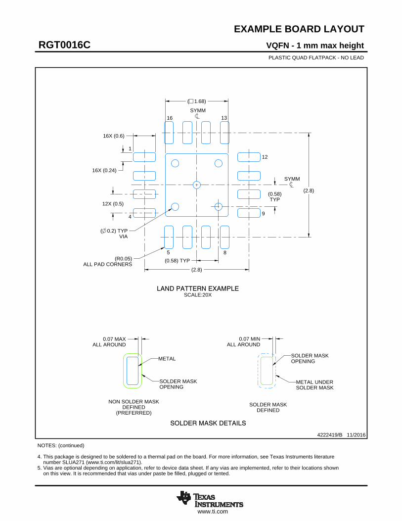
www.ti.com
EXAMPLE BOARD LAYOUT
0.07 MINALL AROUND
0.07 MAXALL AROUND
16X (0.24)
16X (0.6)
( 0.2) TYPVIA
12X (0.5)
(2.8)
(2.8)
(0.58)TYP
( 1.68)
(R0.05)ALL PAD CORNERS
(0.58) TYP
VQFN - 1 mm max heightRGT0016CPLASTIC QUAD FLATPACK - NO LEAD
4222419/B 11/2016
SYMM
1
4
5 8
9
12
1316
SYMM
LAND PATTERN EXAMPLESCALE:20X
NOTES: (continued) 4. This package is designed to be soldered to a thermal pad on the board. For more information, see Texas Instruments literature number SLUA271 (www.ti.com/lit/slua271).5. Vias are optional depending on application, refer to device data sheet. If any vias are implemented, refer to their locations shown on this view. It is recommended that vias under paste be filled, plugged or tented.
SOLDER MASKOPENING
METAL UNDERSOLDER MASK
SOLDER MASKDEFINED
METAL
SOLDER MASKOPENING
SOLDER MASK DETAILS
NON SOLDER MASKDEFINED
(PREFERRED)
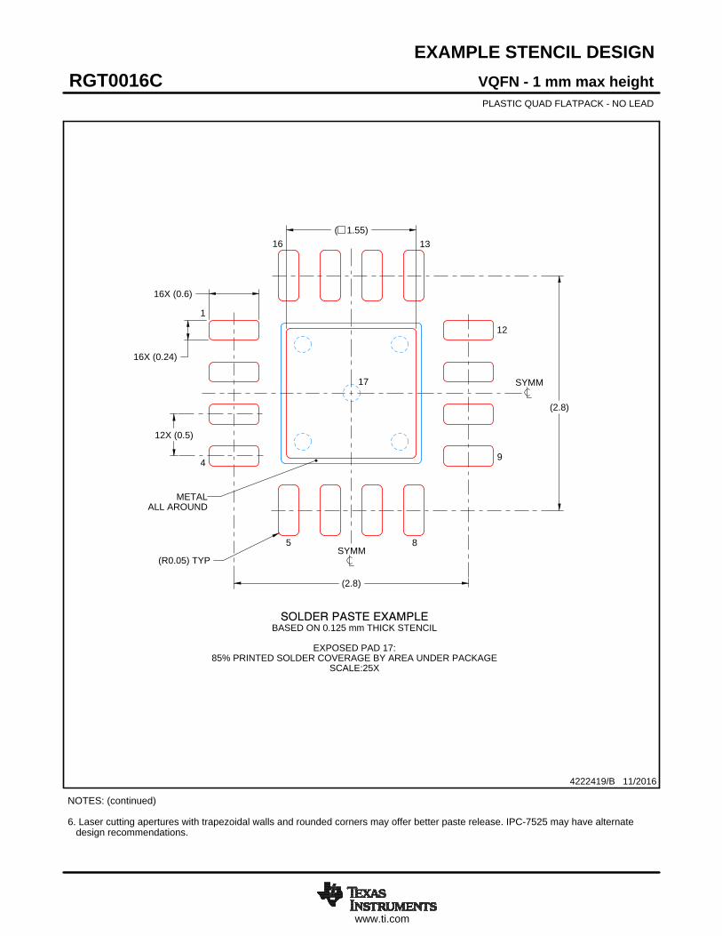
www.ti.com
EXAMPLE STENCIL DESIGN
16X (0.6)
16X (0.24)
12X (0.5)
(2.8)
(2.8)
( 1.55)
(R0.05) TYP
VQFN - 1 mm max heightRGT0016CPLASTIC QUAD FLATPACK - NO LEAD
4222419/B 11/2016
NOTES: (continued) 6. Laser cutting apertures with trapezoidal walls and rounded corners may offer better paste release. IPC-7525 may have alternate design recommendations.
SYMM
ALL AROUNDMETAL
SOLDER PASTE EXAMPLEBASED ON 0.125 mm THICK STENCIL
EXPOSED PAD 17:
85% PRINTED SOLDER COVERAGE BY AREA UNDER PACKAGESCALE:25X
SYMM
1
4
5 8
9
12
1316
17

IMPORTANT NOTICE
Texas Instruments Incorporated (TI) reserves the right to make corrections, enhancements, improvements and other changes to itssemiconductor products and services per JESD46, latest issue, and to discontinue any product or service per JESD48, latest issue. Buyersshould obtain the latest relevant information before placing orders and should verify that such information is current and complete.TI’s published terms of sale for semiconductor products (http://www.ti.com/sc/docs/stdterms.htm) apply to the sale of packaged integratedcircuit products that TI has qualified and released to market. Additional terms may apply to the use or sale of other types of TI products andservices.Reproduction of significant portions of TI information in TI data sheets is permissible only if reproduction is without alteration and isaccompanied by all associated warranties, conditions, limitations, and notices. TI is not responsible or liable for such reproduceddocumentation. Information of third parties may be subject to additional restrictions. Resale of TI products or services with statementsdifferent from or beyond the parameters stated by TI for that product or service voids all express and any implied warranties for theassociated TI product or service and is an unfair and deceptive business practice. TI is not responsible or liable for any such statements.Buyers and others who are developing systems that incorporate TI products (collectively, “Designers”) understand and agree that Designersremain responsible for using their independent analysis, evaluation and judgment in designing their applications and that Designers havefull and exclusive responsibility to assure the safety of Designers' applications and compliance of their applications (and of all TI productsused in or for Designers’ applications) with all applicable regulations, laws and other applicable requirements. Designer represents that, withrespect to their applications, Designer has all the necessary expertise to create and implement safeguards that (1) anticipate dangerousconsequences of failures, (2) monitor failures and their consequences, and (3) lessen the likelihood of failures that might cause harm andtake appropriate actions. Designer agrees that prior to using or distributing any applications that include TI products, Designer willthoroughly test such applications and the functionality of such TI products as used in such applications.TI’s provision of technical, application or other design advice, quality characterization, reliability data or other services or information,including, but not limited to, reference designs and materials relating to evaluation modules, (collectively, “TI Resources”) are intended toassist designers who are developing applications that incorporate TI products; by downloading, accessing or using TI Resources in anyway, Designer (individually or, if Designer is acting on behalf of a company, Designer’s company) agrees to use any particular TI Resourcesolely for this purpose and subject to the terms of this Notice.TI’s provision of TI Resources does not expand or otherwise alter TI’s applicable published warranties or warranty disclaimers for TIproducts, and no additional obligations or liabilities arise from TI providing such TI Resources. TI reserves the right to make corrections,enhancements, improvements and other changes to its TI Resources. TI has not conducted any testing other than that specificallydescribed in the published documentation for a particular TI Resource.Designer is authorized to use, copy and modify any individual TI Resource only in connection with the development of applications thatinclude the TI product(s) identified in such TI Resource. NO OTHER LICENSE, EXPRESS OR IMPLIED, BY ESTOPPEL OR OTHERWISETO ANY OTHER TI INTELLECTUAL PROPERTY RIGHT, AND NO LICENSE TO ANY TECHNOLOGY OR INTELLECTUAL PROPERTYRIGHT OF TI OR ANY THIRD PARTY IS GRANTED HEREIN, including but not limited to any patent right, copyright, mask work right, orother intellectual property right relating to any combination, machine, or process in which TI products or services are used. Informationregarding or referencing third-party products or services does not constitute a license to use such products or services, or a warranty orendorsement thereof. Use of TI Resources may require a license from a third party under the patents or other intellectual property of thethird party, or a license from TI under the patents or other intellectual property of TI.TI RESOURCES ARE PROVIDED “AS IS” AND WITH ALL FAULTS. TI DISCLAIMS ALL OTHER WARRANTIES ORREPRESENTATIONS, EXPRESS OR IMPLIED, REGARDING RESOURCES OR USE THEREOF, INCLUDING BUT NOT LIMITED TOACCURACY OR COMPLETENESS, TITLE, ANY EPIDEMIC FAILURE WARRANTY AND ANY IMPLIED WARRANTIES OFMERCHANTABILITY, FITNESS FOR A PARTICULAR PURPOSE, AND NON-INFRINGEMENT OF ANY THIRD PARTY INTELLECTUALPROPERTY RIGHTS. TI SHALL NOT BE LIABLE FOR AND SHALL NOT DEFEND OR INDEMNIFY DESIGNER AGAINST ANY CLAIM,INCLUDING BUT NOT LIMITED TO ANY INFRINGEMENT CLAIM THAT RELATES TO OR IS BASED ON ANY COMBINATION OFPRODUCTS EVEN IF DESCRIBED IN TI RESOURCES OR OTHERWISE. IN NO EVENT SHALL TI BE LIABLE FOR ANY ACTUAL,DIRECT, SPECIAL, COLLATERAL, INDIRECT, PUNITIVE, INCIDENTAL, CONSEQUENTIAL OR EXEMPLARY DAMAGES INCONNECTION WITH OR ARISING OUT OF TI RESOURCES OR USE THEREOF, AND REGARDLESS OF WHETHER TI HAS BEENADVISED OF THE POSSIBILITY OF SUCH DAMAGES.Unless TI has explicitly designated an individual product as meeting the requirements of a particular industry standard (e.g., ISO/TS 16949and ISO 26262), TI is not responsible for any failure to meet such industry standard requirements.Where TI specifically promotes products as facilitating functional safety or as compliant with industry functional safety standards, suchproducts are intended to help enable customers to design and create their own applications that meet applicable functional safety standardsand requirements. Using products in an application does not by itself establish any safety features in the application. Designers mustensure compliance with safety-related requirements and standards applicable to their applications. Designer may not use any TI products inlife-critical medical equipment unless authorized officers of the parties have executed a special contract specifically governing such use.Life-critical medical equipment is medical equipment where failure of such equipment would cause serious bodily injury or death (e.g., lifesupport, pacemakers, defibrillators, heart pumps, neurostimulators, and implantables). Such equipment includes, without limitation, allmedical devices identified by the U.S. Food and Drug Administration as Class III devices and equivalent classifications outside the U.S.TI may expressly designate certain products as completing a particular qualification (e.g., Q100, Military Grade, or Enhanced Product).Designers agree that it has the necessary expertise to select the product with the appropriate qualification designation for their applicationsand that proper product selection is at Designers’ own risk. Designers are solely responsible for compliance with all legal and regulatoryrequirements in connection with such selection.Designer will fully indemnify TI and its representatives against any damages, costs, losses, and/or liabilities arising out of Designer’s non-compliance with the terms and provisions of this Notice.
Mailing Address: Texas Instruments, Post Office Box 655303, Dallas, Texas 75265Copyright © 2017, Texas Instruments Incorporated


![Finite Element Clifford Algebra: A New Toolkit for ...ccom.ucsd.edu/~agillette/research/pd11talk.pdf · [0;T] k+2 [0;T] k+1 d 6 (r k d 6 (r k k 1 d 6 (r k 2 Finite Element Clifford](https://static.fdocument.org/doc/165x107/5f58bc148149db2e4503093f/finite-element-clifford-algebra-a-new-toolkit-for-ccomucsdeduagilletteresearch.jpg)
![Finite Element Clifford Algebra: A New Toolkit for ...math.arizona.edu/~agillette/research/pd11talk.pdf · [0;T] k+2 [0;T] k+1 d 6 (r k d 6 (r k k 1 d 6 (r k 2 Finite Element Clifford](https://static.fdocument.org/doc/165x107/5f58c22634ae8b00ca3fa708/finite-element-clifford-algebra-a-new-toolkit-for-math-agilletteresearchpd11talkpdf.jpg)