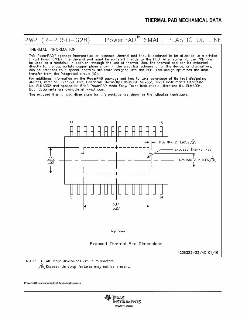
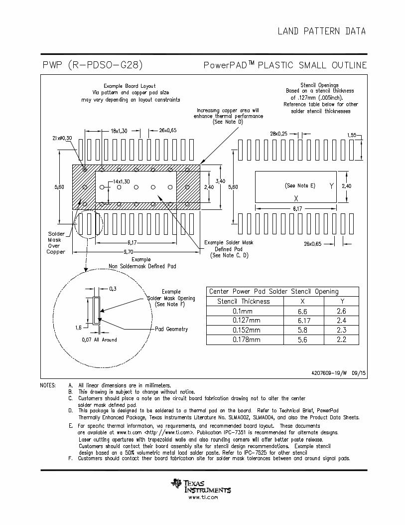
TPA3112D1 25-W Filter-Free Mono Class-D Audio Power ... · 1 2 3 4 5 6 7 8 9 10 28 27 26 25 24 23...
33
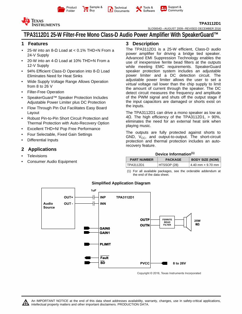
INP INN SD SD Fault Fault PLIMIT PLIMIT PVCC 8 to 26V 1uF OUTN FERRITE BEAD FILTER OUTP 25W 8Ω OUTN FERRITE BEAD FILTER FERRITE BEAD FILTER OUTP 8Ω OUT+ - OUT Audio Source TPA3112D1 GAIN0 GAIN0 GAIN1 GAIN1 Copyright © 2016, Texas Instruments Incorporated Product Folder Sample & Buy Technical Documents Tools & Software Support & Community An IMPORTANT NOTICE at the end of this data sheet addresses availability, warranty, changes, use in safety-critical applications, intellectual property matters and other important disclaimers. PRODUCTION DATA. TPA3112D1 SLOS654D – AUGUST 2009 – REVISED DECEMBER 2016 TPA3112D1 25-W Filter-Free Mono Class-D Audio Power Amplifier With SpeakerGuard™ 1 1 Features 1• 25-W into an 8-Ω Load at < 0.1% THD+N From a 24-V Supply • 20-W into an 4-Ω Load at 10% THD+N From a 12-V Supply • 94% Efficient Class-D Operation into 8-Ω Load Eliminates Need for Heat Sinks • Wide Supply Voltage Range Allows Operation from 8 to 26 V • Filter-Free Operation • SpeakerGuard™ Speaker Protection Includes Adjustable Power Limiter plus DC Protection • Flow Through Pin Out Facilitates Easy Board Layout • Robust Pin-to-Pin Short Circuit Protection and Thermal Protection with Auto-Recovery Option • Excellent THD+N/ Pop Free Performance • Four Selectable, Fixed Gain Settings • Differential Inputs 2 Applications • Televisions • Consumer Audio Equipment 3 Description The TPA3112D1 is a 25-W efficient, Class-D audio power amplifier for driving a bridge tied speaker. Advanced EMI Suppression Technology enables the use of inexpensive ferrite bead filters at the outputs while meeting EMC requirements. SpeakerGuard speaker protection system includes an adjustable power limiter and a DC detection circuit. The adjustable power limiter allows the user to set a virtual voltage rail lower than the chip supply to limit the amount of current through the speaker. The DC detect circuit measures the frequency and amplitude of the PWM signal and shuts off the output stage if the input capacitors are damaged or shorts exist on the inputs. The TPA3112D1 can drive a mono speaker as low as 4Ω. The high efficiency of the TPA3112D1, > 90%, eliminates the need for an external heat sink when playing music. The outputs are fully protected against shorts to GND, V CC , and output-to-output. The short-circuit protection and thermal protection includes an auto- recovery feature. Device Information (1) PART NUMBER PACKAGE BODY SIZE (NOM) TPA3112D1 HTSSOP (28) 4.40 mm × 9.70 mm (1) For all available packages, see the orderable addendum at the end of the data sheet. Simplified Application Diagram
Transcript of TPA3112D1 25-W Filter-Free Mono Class-D Audio Power ... · 1 2 3 4 5 6 7 8 9 10 28 27 26 25 24 23...
INP
INN
SDSD
FaultFault
PLIMITPLIMIT
PVCC 8 to 26V
1uF
OUTN
FERRITE
BEAD
FILTER
OUTP 25W
8ΩOUTN
FERRITE
BEAD
FILTER
FERRITE
BEAD
FILTER
OUTP
8Ω
OUT+
-OUTAudio
Source
TPA3112D1
GAIN0GAIN0
GAIN1GAIN1
Copyright © 2016, Texas Instruments Incorporated
Product
Folder
Sample &Buy
Technical
Documents
Tools &
Software
Support &Community
An IMPORTANT NOTICE at the end of this data sheet addresses availability, warranty, changes, use in safety-critical applications,intellectual property matters and other important disclaimers. PRODUCTION DATA.
TPA3112D1SLOS654D –AUGUST 2009–REVISED DECEMBER 2016
TPA3112D1 25-W Filter-Free Mono Class-D Audio Power Amplifier With SpeakerGuard™
1
1 Features1• 25-W into an 8-Ω Load at < 0.1% THD+N From a
24-V Supply• 20-W into an 4-Ω Load at 10% THD+N From a
12-V Supply• 94% Efficient Class-D Operation into 8-Ω Load
Eliminates Need for Heat Sinks• Wide Supply Voltage Range Allows Operation
from 8 to 26 V• Filter-Free Operation• SpeakerGuard™ Speaker Protection Includes
Adjustable Power Limiter plus DC Protection• Flow Through Pin Out Facilitates Easy Board
Layout• Robust Pin-to-Pin Short Circuit Protection and
Thermal Protection with Auto-Recovery Option• Excellent THD+N/ Pop Free Performance• Four Selectable, Fixed Gain Settings• Differential Inputs
2 Applications• Televisions• Consumer Audio Equipment
3 DescriptionThe TPA3112D1 is a 25-W efficient, Class-D audiopower amplifier for driving a bridge tied speaker.Advanced EMI Suppression Technology enables theuse of inexpensive ferrite bead filters at the outputswhile meeting EMC requirements. SpeakerGuardspeaker protection system includes an adjustablepower limiter and a DC detection circuit. Theadjustable power limiter allows the user to set avirtual voltage rail lower than the chip supply to limitthe amount of current through the speaker. The DCdetect circuit measures the frequency and amplitudeof the PWM signal and shuts off the output stage ifthe input capacitors are damaged or shorts exist onthe inputs.
The TPA3112D1 can drive a mono speaker as low as4Ω. The high efficiency of the TPA3112D1, > 90%,eliminates the need for an external heat sink whenplaying music.
The outputs are fully protected against shorts toGND, VCC, and output-to-output. The short-circuitprotection and thermal protection includes an auto-recovery feature.
Device Information(1)
PART NUMBER PACKAGE BODY SIZE (NOM)TPA3112D1 HTSSOP (28) 4.40 mm × 9.70 mm
(1) For all available packages, see the orderable addendum atthe end of the data sheet.
Simplified Application Diagram
2
TPA3112D1SLOS654D –AUGUST 2009–REVISED DECEMBER 2016 www.ti.com
Product Folder Links: TPA3112D1
Submit Documentation Feedback Copyright © 2009–2016, Texas Instruments Incorporated
Table of Contents1 Features .................................................................. 12 Applications ........................................................... 13 Description ............................................................. 14 Revision History..................................................... 25 Pin Configuration and Functions ......................... 36 Specifications......................................................... 4
6.1 Absolute Maximum Ratings ..................................... 46.2 ESD Ratings ............................................................ 46.3 Recommended Operating Conditions...................... 46.4 Thermal Information ................................................. 56.5 DC Characteristics, VCC = 24 V............................... 56.6 DC Characteristics, VCC = 12 V............................... 56.7 AC Characteristics, VCC = 24 V ............................... 66.8 AC Characteristics, VCC = 12 V ............................... 66.9 Typical Characteristics .............................................. 7
7 Detailed Description ............................................ 107.1 Overview ................................................................. 107.2 Functional Block Diagram ....................................... 11
7.3 Feature Description................................................. 117.4 Device Functional Modes........................................ 14
8 Application and Implementation ........................ 168.1 Application Information............................................ 168.2 Typical Application ................................................. 16
9 Power Supply Recommendations ...................... 2110 Layout................................................................... 22
10.1 Layout Guidelines ................................................. 2210.2 Layout Example .................................................... 23
11 Device and Documentation Support ................. 2411.1 Device Support .................................................... 2411.2 Documentation Support ....................................... 2411.3 Recieving Notification of Documentation Updates 2411.4 Community Resources.......................................... 2411.5 Trademarks ........................................................... 2411.6 Electrostatic Discharge Caution............................ 2411.7 Glossary ................................................................ 24
12 Mechanical, Packaging, and OrderableInformation ........................................................... 25
4 Revision HistoryNOTE: Page numbers for previous revisions may differ from page numbers in the current version.
Changes from Revision C (July 2012) to Revision D Page
• Added Device Information table, ESD Ratings table, Feature Description section, Device Functional Modes,Application and Implementation section, Power Supply Recommendations section, Layout section, Device andDocumentation Support section, and Mechanical, Packaging, and Orderable Information section. .................................... 1
1
2
3
4
5
6
7
8
9
10
28
27
26
25
24
23
22
21
20
19
SD
FAULT
GND
GND
GAIN0
GAIN1
AVCC
AGND
GVDD
PLIMIT
PVCC
PVCC
BSN
OUTN
PGND
OUTN
BSN
BSP
OUTP
PGND
INN
INP
NC
11
12
13
14
18
17
16
15
OUTP
BSP
PVCC
PVCCAVCC
3
TPA3112D1www.ti.com SLOS654D –AUGUST 2009–REVISED DECEMBER 2016
Product Folder Links: TPA3112D1
Submit Documentation FeedbackCopyright © 2009–2016, Texas Instruments Incorporated
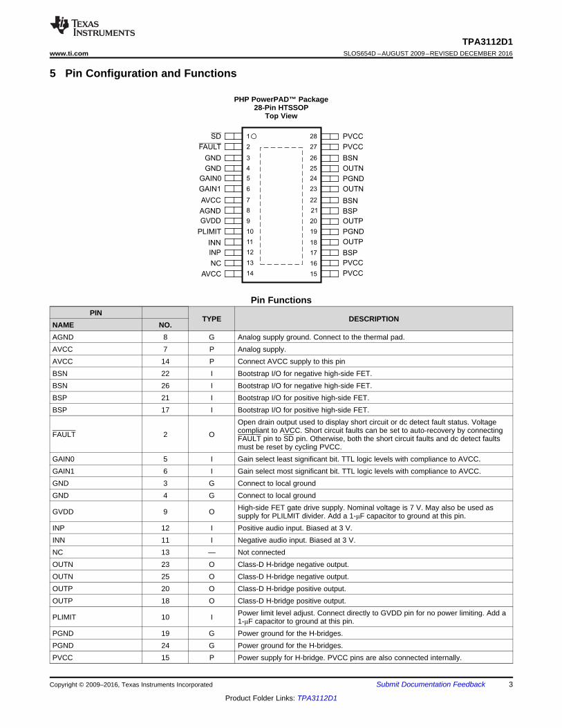
5 Pin Configuration and Functions
PHP PowerPAD™ Package28-Pin HTSSOP
Top View
Pin FunctionsPIN
TYPE DESCRIPTIONNAME NO.AGND 8 G Analog supply ground. Connect to the thermal pad.AVCC 7 P Analog supply.AVCC 14 P Connect AVCC supply to this pinBSN 22 I Bootstrap I/O for negative high-side FET.BSN 26 I Bootstrap I/O for negative high-side FET.BSP 21 I Bootstrap I/O for positive high-side FET.BSP 17 I Bootstrap I/O for positive high-side FET.
FAULT 2 O
Open drain output used to display short circuit or dc detect fault status. Voltagecompliant to AVCC. Short circuit faults can be set to auto-recovery by connectingFAULT pin to SD pin. Otherwise, both the short circuit faults and dc detect faultsmust be reset by cycling PVCC.
GAIN0 5 I Gain select least significant bit. TTL logic levels with compliance to AVCC.GAIN1 6 I Gain select most significant bit. TTL logic levels with compliance to AVCC.GND 3 G Connect to local groundGND 4 G Connect to local ground
GVDD 9 O High-side FET gate drive supply. Nominal voltage is 7 V. May also be used assupply for PLILMIT divider. Add a 1-μF capacitor to ground at this pin.
INP 12 I Positive audio input. Biased at 3 V.INN 11 I Negative audio input. Biased at 3 V.NC 13 — Not connectedOUTN 23 O Class-D H-bridge negative output.OUTN 25 O Class-D H-bridge negative output.OUTP 20 O Class-D H-bridge positive output.OUTP 18 O Class-D H-bridge positive output.
PLIMIT 10 I Power limit level adjust. Connect directly to GVDD pin for no power limiting. Add a1-μF capacitor to ground at this pin.
PGND 19 G Power ground for the H-bridges.PGND 24 G Power ground for the H-bridges.PVCC 15 P Power supply for H-bridge. PVCC pins are also connected internally.
4
TPA3112D1SLOS654D –AUGUST 2009–REVISED DECEMBER 2016 www.ti.com
Product Folder Links: TPA3112D1
Submit Documentation Feedback Copyright © 2009–2016, Texas Instruments Incorporated
Pin Functions (continued)PIN
TYPE DESCRIPTIONNAME NO.PVCC 16 P Power supply for H-bridge. PVCC pins are also connected internally.PVCC 27 P Power supply for H-bridge. PVCC pins are also connected internally.PVCC 28 P Power supply for H-bridge. PVCC pins are also connected internally.
SD 1 I Shutdown logic input for audio amp (LOW = outputs Hi-Z, HIGH = outputsenabled). TTL logic levels with compliance to AVCC.
(1) Stresses beyond those listed under absolute maximum ratings may cause permanent damage to the device. These are stress ratingsonly, and functional operations of the device at these or any other conditions beyond those indicated under recommended operatingconditions is not implied. Exposure to absolute-maximum-rated conditions for extended periods may affect device reliability.
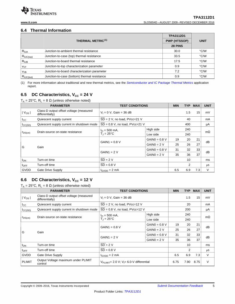
6 Specifications
6.1 Absolute Maximum Ratingsover operating free-air temperature range (unless otherwise noted) (1)
MIN MAX UNITVCC Supply voltage AVCC, PVCC –0.3 30 V
VI Interface pin voltage
SD, FAULT,GAIN0, GAIN1, AVCC (Pin14)
–0.3 VCC + 0.3 V< 10 V/ms
PLIMIT –0.3 GVDD + 0.3 VINN, INP –0.3 6.3 V
TA Operating free-air temperature –40 85 °CRL Minimum Load Resistance BTL 3.2 Ω
Tstg DMD storage temperature –65 150 °C
(1) JEDEC document JEP155 states that 500-V HBM allows safe manufacturing with a standard ESD control process.(2) JEDEC document JEP157 states that 250-V CDM allows safe manufacturing with a standard ESD control process.
6.2 ESD RatingsVALUE UNIT
V(ESD) Electrostatic dischargeHuman-body model (HBM), per ANSI/ESDA/JEDEC JS-001 (1) ±2000
VCharged-device model (CDM), per JEDEC specification JESD22-C101 (2) ±500
6.3 Recommended Operating Conditionsover operating free-air temperature range (unless otherwise noted)
MIN NOM MAX UNITVCC Supply voltage PVCC, AVCC 8 26 VVIH High-level input voltage SD, GAIN0, GAIN1 2 VVIL Low-level input voltage SD, GAIN0, GAIN1 0.8 VVOL Low-level output voltage FAULT, RPULLUP = 100 kΩ, VCC = 26 V 0.8 VIIH High-level input current SD, GAIN0, GAIN1, VI = 2 V, VCC = 18 V 50 µAIIL Low-level input current SD, GAIN0, GAIN1, VI = 0.8 V, VCC = 18 V 5 µA
5
TPA3112D1www.ti.com SLOS654D –AUGUST 2009–REVISED DECEMBER 2016
Product Folder Links: TPA3112D1
Submit Documentation FeedbackCopyright © 2009–2016, Texas Instruments Incorporated
(1) For more information about traditional and new thermal metrics, see the Semiconductor and IC Package Thermal Metrics applicationreport.
6.4 Thermal Information
THERMAL METRIC (1)TPA3112D1
UNITPWP (HTSSOP)28 PINS
RθJA Junction-to-ambient thermal resistance 30.0 °C/WRθJC(top) Junction-to-case (top) thermal resistance 33.5 °C/WRθJB Junction-to-board thermal resistance 17.5 °C/WψJT Junction-to-top characterization parameter 0.9 °C/WψJB Junction-to-board characterization parameter 7.2 °C/WRθJC(bot) Junction-to-case (bottom) thermal resistance 0.9 °C/W
6.5 DC Characteristics, VCC = 24 VTA = 25°C, RL = 8 Ω (unless otherwise noted)
PARAMETER TEST CONDITIONS MIN TYP MAX UNIT
| VOS | Class-D output offset voltage (measureddifferentially) VI = 0 V, Gain = 36 dB 1.5 15 mV
ICC Quiescent supply current SD = 2 V, no load, PVcc=21 V 40 mAICC(SD) Quiescent supply current in shutdown mode SD = 0.8 V, no load, PVcc=21 V 400 µA
rDS(on) Drain-source on-state resistance IO = 500 mA,TJ = 25°C
High side 240mΩ
Low side 240
G GainGAIN1 = 0.8 V
GAIN0 = 0.8 V 19 20 21dB
GAIN0 = 2 V 25 26 27
GAIN1 = 2 VGAIN0 = 0.8 V 31 32 33
dBGAIN0 = 2 V 35 36 37
tON Turn-on time SD = 2 V 10 mstOFF Turn-off time SD = 0.8 V 2 μsGVDD Gate Drive Supply IGVDD = 2 mA 6.5 6.9 7.3 V
6.6 DC Characteristics, VCC = 12 VTA = 25°C, RL = 8 Ω (unless otherwise noted)
PARAMETER TEST CONDITIONS MIN TYP MAX UNIT
| VOS | Class-D output offset voltage (measureddifferentially) VI = 0 V, Gain = 36 dB 1.5 15 mV
ICC Quiescent supply current SD = 2 V, no load, PVcc=12 V 20 mAICC(SD) Quiescent supply current in shutdown mode SD = 0.8 V, no load, PVcc=12 V 200 µA
rDS(on) Drain-source on-state resistance IO = 500 mA,TJ = 25°C
High side 240mΩ
Low side 240
G GainGAIN1 = 0.8 V
GAIN0 = 0.8 V 19 20 21dB
GAIN0 = 2 V 25 26 27
GAIN1 = 2 VGAIN0 = 0.8 V 31 32 33
dBGAIN0 = 2 V 35 36 37
tON Turn-on time SD = 2 V 10 mstOFF Turn-off time SD = 0.8 V 2 μsGVDD Gate Drive Supply IGVDD = 2 mA 6.5 6.9 7.3 V
PLIMIT Output Voltage maximum under PLIMITcontrol VPLIMIT= 2.0 V; VI= 6.0-V differential 6.75 7.90 8.75 V
6
TPA3112D1SLOS654D –AUGUST 2009–REVISED DECEMBER 2016 www.ti.com
Product Folder Links: TPA3112D1
Submit Documentation Feedback Copyright © 2009–2016, Texas Instruments Incorporated
6.7 AC Characteristics, VCC = 24 VTA = 25°C, RL = 8 Ω (unless otherwise noted)
PARAMETER TEST CONDITIONS MIN TYP MAX UNIT
KSVR Power Supply ripple rejection 200-mVPP ripple from 20 Hz–1 kHz,Gain = 20 dB, Inputs AC-coupled to AGND –70 dB
PO Continuous output power THD+N ≤ 0.1%, f = 1 kHz, VCC = 24 V 25 W
THD+N Total harmonic distortion + noise VCC = 24 V, f = 1 kHz, PO = 12 W (half-power) <0.05%
Vn Output integrated noise 20 Hz to 22 kHz, A-weighted filter, Gain = 20 dB65 µV
–80 dBVCrosstalk VO = 1 Vrms, Gain = 20 dB, f = 1 kHz –70 dB
SNR Signal-to-noise ratio Maximum output at THD+N < 1%, f = 1 kHz,Gain = 20 dB, A-weighted 102 dB
fOSC Oscillator frequency 250 310 350 kHzThermal trip point 150 °CThermal hysteresis 15 °C
6.8 AC Characteristics, VCC = 12 VTA = 25°C, RL = 8 Ω (unless otherwise noted)
PARAMETER TEST CONDITIONS MIN TYP MAX UNIT
KSVR Supply ripple rejection 200-mVPP ripple from 20 Hz–1 kHz,Gain = 20 dB, Inputs ac-coupled to AGND –70 dB
PO Continuous output power THD+N ≤ 10%, f = 1 kHz , RL = 8 Ω 10 WPO Continuous output power THD+N ≤ 10%, f = 1 kHz , RL = 4 Ω 20 W
THD+N Total harmonic distortion + noise RL = 8 Ω, f = 1 kHz, PO = 5 W (half-power) <0.06%
Vn Output integrated noise 20 Hz to 22 kHz, A-weighted filter, Gain = 20 dB65 µV
–80 dBVCrosstalk Po = 1 W, Gain = 20 dB, f = 1 kHz –70 dB
SNR Signal-to-noise ratio Maximum output at THD+N < 1%, f = 1 kHz,Gain = 20 dB, A-weighted 102 dB
fOSC Oscillator frequency 250 310 350 kHzThermal trip point 150 °CThermal hysteresis 15 °C
PO − Output Power − W
TH
D+
N−
Tota
l H
arm
onic
Dis
tort
ion
+ N
ois
e−
%
0.001
0.1
10
0.01
1
G005
f = 1 kHz
Gain = 20 dB
VCC = 24 V
ZL = 8 Ω + 66 µH
f = 20 Hz
0.01 0.1 1 3010
f = 10 kHz
PO − Output Power − W
TH
D+
N−
Tota
l H
arm
onic
Dis
tort
ion
+ N
ois
e−
%
0.001
0.1
10
0.01
1
G006
f = 1 kHz
Gain = 20 dB
VCC = 12 V
ZL = 4 Ω + 33 µH
f = 20 Hz
f = 10 kHz
0.01 0.1 1 3010
f − Frequency − Hz
20 100 1k 10k
TH
D−
Tota
l H
arm
onic
Dis
tort
ion
−%
0.001
0.1
10
20k
0.01
1
G003
PO = 10 W
PO = 1 W
PO = 5 W
PO − Output Power − W
0.01 0.1 1
TH
D+
N−
Tota
l H
arm
onic
Dis
tort
ion
+ N
ois
e−
%
0.001
0.1
10
30
0.01
1
G004
f = 1 kHz
Gain = 20 dB
VCC = 12 V
ZL = 8 Ω + 66 µH
f = 20 Hz
f = 10 kHz
10
f − Frequency − Hz
20 100 1k 10k
TH
D−
Tota
l H
arm
onic
Dis
tort
ion
−%
0.001
0.1
10
20k
0.01
1
G001
PO = 2.5 W
PO = 5 W
PO = 1 W
f − Frequency − Hz
20 100 1k 10k
TH
D−
Tota
l H
arm
onic
Dis
tort
ion
−%
0.001
0.1
10
20k
0.01
1
G002
PO = 10 W
PO = 5 W
PO = 1 W
7
TPA3112D1www.ti.com SLOS654D –AUGUST 2009–REVISED DECEMBER 2016
Product Folder Links: TPA3112D1
Submit Documentation FeedbackCopyright © 2009–2016, Texas Instruments Incorporated
6.9 Typical Characteristics(All Measurements taken at 1 kHz, unless otherwise noted. Measurements were made using the TPA3112D2 EVM which isavailable at ti.com.)
Gain = 20 dB VCC = 12 V ZL = 8 Ω + 66 µH
Figure 1. Total Harmonic Distortion vs Frequency
Gain = 20 dB VCC = 24 V ZL = 8 Ω + 66 µH
Figure 2. Total Harmonic Distortion vs Frequency
Gain = 20 dB VCC = 12 V ZL = 4 Ω + 33 µH
Figure 3. Total Harmonic Distortion vs Frequency
Gain = 20 dB VCC = 12 V ZL = 8 Ω + 66 µH
Figure 4. Total Harmonic Distortion + Noise vs OutputPower
Gain = 20 dB VCC = 24 V ZL = 8 Ω + 66 µH
Figure 5. Total Harmonic Distortion + Noise vs OutputPower
Gain = 20 dB VCC = 12 V ZL = 4 Ω + 33 µH
Figure 6. Total Harmonic Distortion + Noise vs OutputPower
PO − Output Power − W
0
10
20
30
40
50
60
70
80
90
100
0 5 10 15 20 25 30
h−
Effi
cie
ncy
−%
G013
Gain = 20 dB
ZL = 4 Ω + 33 µH
VCC = 24 V
VCC = 12 V
PO(Tot) − Total Output Power − W
0.0
0.2
0.4
0.6
0.8
1.0
1.2
0 5 10 15 20 25 30
I CC
−S
upply
Curr
ent−
A
G014
VCC = 12 V
VCC = 24 V
Gain = 20 dB
ZL = 8 Ω + 66 µH
f − Frequency − Hz
Phase
−°
100
50
0
−3000
5
10
15
20
25
30
35
40
Gain
−dB
−50
−100
−150
10 100 10k 100k1k
G009
Phase
Gain
−200
−250
PO − Output Power − W
0
10
20
30
40
50
60
70
80
90
100
0 5 10 15 20 25 30
h−
Effi
cie
ncy
−%
G012
VCC = 24 V
Gain = 20 dB
ZL = 8 Ω + 66 µH
VCC = 12 V
VPLIMIT − PLIMIT Voltage − V
0
5
10
15
20
25
30
0.0 0.5 1.0 1.5 2.0 2.5 3.0 3.5 4.0 4.5 5.0
PO
(Max)−
Maxim
um
Outp
ut
Pow
er
−W
G007
Gain = 20 dB
VCC = 24 V
ZL = 8 Ω + 66 µH
VPLIMIT − PLIMIT Voltage − V
0
5
10
15
20
25
30
0.0 0.5 1.0 1.5 2.0 2.5 3.0 3.5 4.0
PO
−O
utp
ut
Pow
er
−W
G008
Gain = 20 dB
VCC = 12 V
ZL = 4 Ω + 33 µH
8
TPA3112D1SLOS654D –AUGUST 2009–REVISED DECEMBER 2016 www.ti.com
Product Folder Links: TPA3112D1
Submit Documentation Feedback Copyright © 2009–2016, Texas Instruments Incorporated
Typical Characteristics (continued)(All Measurements taken at 1 kHz, unless otherwise noted. Measurements were made using the TPA3112D2 EVM which isavailable at ti.com.)
Gain = 20 dB VCC = 24 V ZL = 8 Ω + 66 µH
Figure 7. Maximum Output Power vs Plimit Voltage
Gain = 20 dB VCC = 12 V ZL = 4 Ω + 33 µH
Figure 8. Output Power vs Plimit Voltage
Gain = 20 dB VCC = 12 V ZL = 8 Ω + 66 µHCI = µF VI = 0.1 VRMS
Figure 9. Gain/Phase vs Frequency
Gain = 20 dB ZL = 8 Ω + 66 µH
Figure 10. Efficiency vs Output Power
Gain = 20 dB ZL = 4 Ω + 33 µH
Figure 11. Efficiency vs Output Power
Gain = 20 dB ZL = 8 Ω + 66 µH
Figure 12. Supply Current vs Total Output Power
PO(Tot) − Total Output Power − W
0.0
0.2
0.4
0.6
0.8
1.0
1.2
1.4
1.6
1.8
0 5 10 15 20 25 30
I CC
−S
upply
Curr
ent−
A
G015
Gain = 20 dB
VCC = 12 V
ZL = 4 Ω + 33 µH
−120
−100
−80
−60
−40
−20
0
f − Frequency − Hz
KS
VR
−S
upply
Rip
ple
Reje
ction
Ratio
−dB
20 100 1k 10k 20k
G016
9
TPA3112D1www.ti.com SLOS654D –AUGUST 2009–REVISED DECEMBER 2016
Product Folder Links: TPA3112D1
Submit Documentation FeedbackCopyright © 2009–2016, Texas Instruments Incorporated
Typical Characteristics (continued)(All Measurements taken at 1 kHz, unless otherwise noted. Measurements were made using the TPA3112D2 EVM which isavailable at ti.com.)
Gain = 20 dB VCC = 12 V ZL = 4 Ω + 33 µH
Figure 13. Supply Current vs Total Output Power
Gain = 20 dB VCC = 12 V ZL = 8 Ω + 66 µH
Figure 14. Supply Ripple Rejection Ratio vs Frequency
10
TPA3112D1SLOS654D –AUGUST 2009–REVISED DECEMBER 2016 www.ti.com
Product Folder Links: TPA3112D1
Submit Documentation Feedback Copyright © 2009–2016, Texas Instruments Incorporated
7 Detailed Description
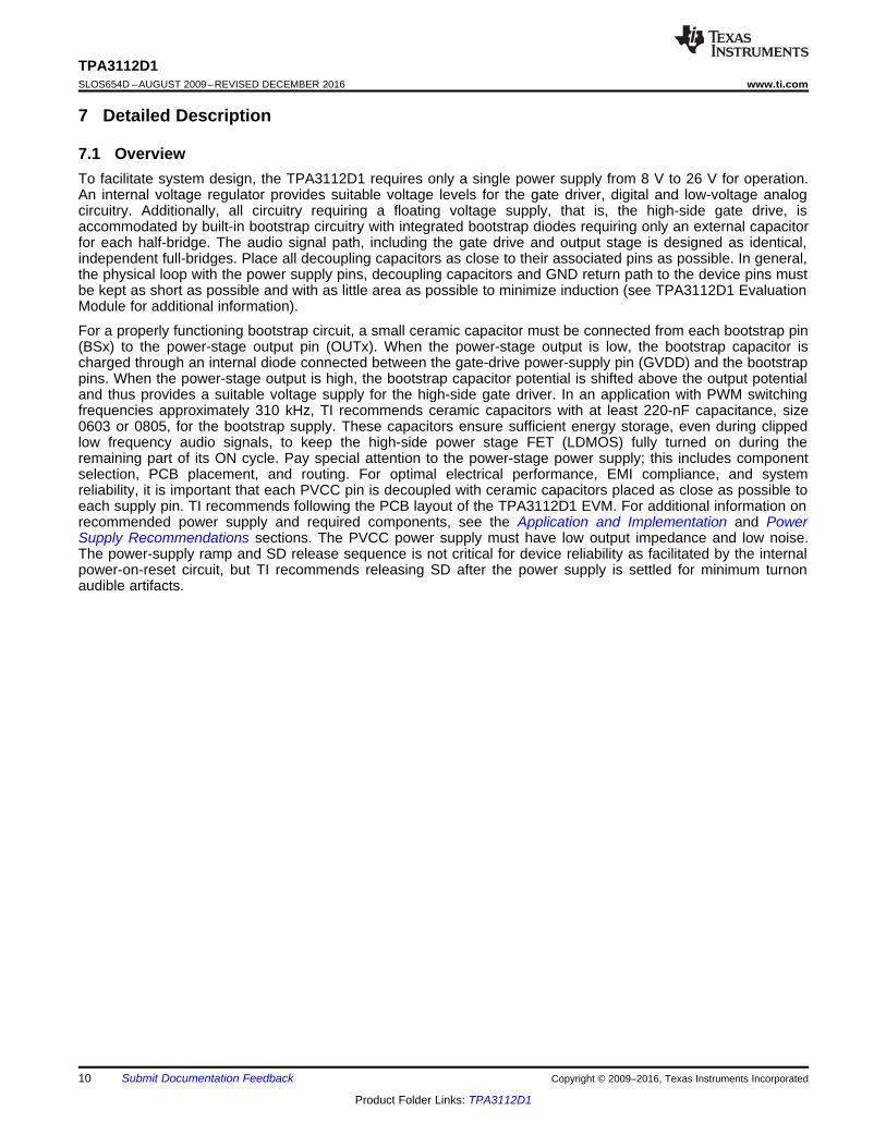
7.1 OverviewTo facilitate system design, the TPA3112D1 requires only a single power supply from 8 V to 26 V for operation.An internal voltage regulator provides suitable voltage levels for the gate driver, digital and low-voltage analogcircuitry. Additionally, all circuitry requiring a floating voltage supply, that is, the high-side gate drive, isaccommodated by built-in bootstrap circuitry with integrated bootstrap diodes requiring only an external capacitorfor each half-bridge. The audio signal path, including the gate drive and output stage is designed as identical,independent full-bridges. Place all decoupling capacitors as close to their associated pins as possible. In general,the physical loop with the power supply pins, decoupling capacitors and GND return path to the device pins mustbe kept as short as possible and with as little area as possible to minimize induction (see TPA3112D1 EvaluationModule for additional information).
For a properly functioning bootstrap circuit, a small ceramic capacitor must be connected from each bootstrap pin(BSx) to the power-stage output pin (OUTx). When the power-stage output is low, the bootstrap capacitor ischarged through an internal diode connected between the gate-drive power-supply pin (GVDD) and the bootstrappins. When the power-stage output is high, the bootstrap capacitor potential is shifted above the output potentialand thus provides a suitable voltage supply for the high-side gate driver. In an application with PWM switchingfrequencies approximately 310 kHz, TI recommends ceramic capacitors with at least 220-nF capacitance, size0603 or 0805, for the bootstrap supply. These capacitors ensure sufficient energy storage, even during clippedlow frequency audio signals, to keep the high-side power stage FET (LDMOS) fully turned on during theremaining part of its ON cycle. Pay special attention to the power-stage power supply; this includes componentselection, PCB placement, and routing. For optimal electrical performance, EMI compliance, and systemreliability, it is important that each PVCC pin is decoupled with ceramic capacitors placed as close as possible toeach supply pin. TI recommends following the PCB layout of the TPA3112D1 EVM. For additional information onrecommended power supply and required components, see the Application and Implementation and PowerSupply Recommendations sections. The PVCC power supply must have low output impedance and low noise.The power-supply ramp and SD release sequence is not critical for device reliability as facilitated by the internalpower-on-reset circuit, but TI recommends releasing SD after the power supply is settled for minimum turnonaudible artifacts.
+
+±
±
+
+±
±
+
±
+
±
PLIMIT
PLIMITReference
Gain Control
TTLBuffer
LDORegulator
Ramp Generator
Biases and References
Startup Protection
Logic
SC Detect
DC Detect
Thermal Detect
UVLO and OVLO
Gate Drive
Gate Drive
PWM Logic
AGND
GVDD
GVDD
AVCC
AVCC
PLIMIT
GAIN1
GAIN0
SD
FAULT
INN
INP
OUTN FB
Gain Control
OUTP FBGVDD
PVCCPVCC
PVCCPVCC
GVDD
OUTN FB
OUTP FB
OUTN
PGND
BSN
PGND
OUTP
BSP
Copyright © 2016, Texas Instruments Incorporated
11
TPA3112D1www.ti.com SLOS654D –AUGUST 2009–REVISED DECEMBER 2016
Product Folder Links: TPA3112D1
Submit Documentation FeedbackCopyright © 2009–2016, Texas Instruments Incorporated
7.2 Functional Block Diagram
7.3 Feature Description
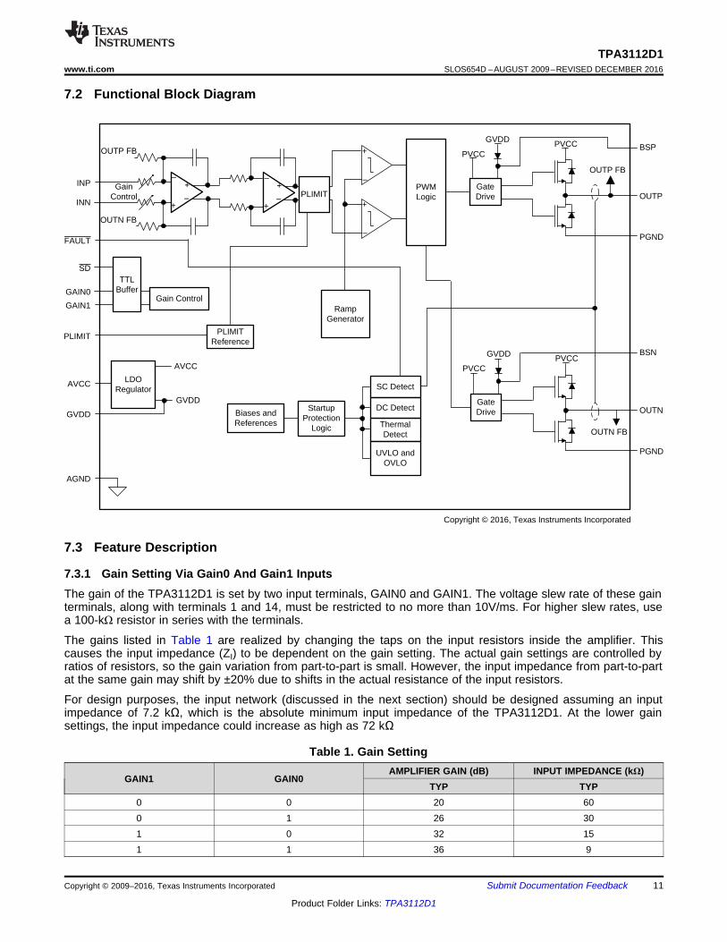
7.3.1 Gain Setting Via Gain0 And Gain1 InputsThe gain of the TPA3112D1 is set by two input terminals, GAIN0 and GAIN1. The voltage slew rate of these gainterminals, along with terminals 1 and 14, must be restricted to no more than 10V/ms. For higher slew rates, usea 100-kΩ resistor in series with the terminals.
The gains listed in Table 1 are realized by changing the taps on the input resistors inside the amplifier. Thiscauses the input impedance (ZI) to be dependent on the gain setting. The actual gain settings are controlled byratios of resistors, so the gain variation from part-to-part is small. However, the input impedance from part-to-partat the same gain may shift by ±20% due to shifts in the actual resistance of the input resistors.
For design purposes, the input network (discussed in the next section) should be designed assuming an inputimpedance of 7.2 kΩ, which is the absolute minimum input impedance of the TPA3112D1. At the lower gainsettings, the input impedance could increase as high as 72 kΩ
Table 1. Gain Setting
GAIN1 GAIN0AMPLIFIER GAIN (dB) INPUT IMPEDANCE (kΩ)
TYP TYP0 0 20 600 1 26 301 0 32 151 1 36 9
TPA3112D1 PLimit Operation
12
TPA3112D1SLOS654D –AUGUST 2009–REVISED DECEMBER 2016 www.ti.com
Product Folder Links: TPA3112D1
Submit Documentation Feedback Copyright © 2009–2016, Texas Instruments Incorporated
7.3.2 SD OperationThe TPA3112D1 employs a shutdown mode of operation designed to reduce supply current (ICC) to the absoluteminimum level during periods of nonuse for power conservation. The SD input terminal should be held high (seespecification table for trip point) during normal operation when the amplifier is in use. Pulling SD low causes theoutputs to mute and the amplifier to enter a low-current state. Never leave SD unconnected, because amplifieroperation would be unpredictable.
For the best power-off pop performance, place the amplifier in the shutdown mode prior to removing the powersupply voltage.
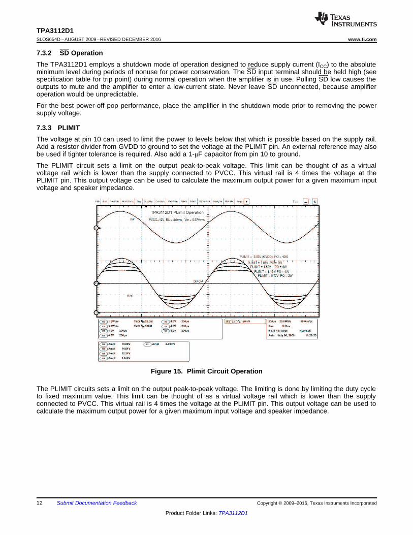
7.3.3 PLIMITThe voltage at pin 10 can used to limit the power to levels below that which is possible based on the supply rail.Add a resistor divider from GVDD to ground to set the voltage at the PLIMIT pin. An external reference may alsobe used if tighter tolerance is required. Also add a 1-μF capacitor from pin 10 to ground.
The PLIMIT circuit sets a limit on the output peak-to-peak voltage. This limit can be thought of as a virtualvoltage rail which is lower than the supply connected to PVCC. This virtual rail is 4 times the voltage at thePLIMIT pin. This output voltage can be used to calculate the maximum output power for a given maximum inputvoltage and speaker impedance.
Figure 15. Plimit Circuit Operation
The PLIMIT circuits sets a limit on the output peak-to-peak voltage. The limiting is done by limiting the duty cycleto fixed maximum value. This limit can be thought of as a virtual voltage rail which is lower than the supplyconnected to PVCC. This virtual rail is 4 times the voltage at the PLIMIT pin. This output voltage can be used tocalculate the maximum output power for a given maximum input voltage and speaker impedance.
2
2
2
LP
L SOUT
L
RV
R RP for unclipped power
R
æ öæ ö´ç ÷ç ÷ç ÷+ ´è øè ø=
´
13
TPA3112D1www.ti.com SLOS654D –AUGUST 2009–REVISED DECEMBER 2016
Product Folder Links: TPA3112D1
Submit Documentation FeedbackCopyright © 2009–2016, Texas Instruments Incorporated
(1)
Where:RS is the total series resistance including RDS(on), and any resistance in the output filter.RL is the load resistance.VP is the peak amplitude of the output possible within the supply rail.
VP = 4 × PLIMIT voltage if PLIMIT < 4 × VPPOUT(10%THD) = 1.25 × POUT(unclipped)
Table 2. Plimit Typical Operation
Test Conditions () PLIMIT Voltage Output Power (W) Output VoltageAmplitude (VP-P)
PVCC=24V, Vin=1Vrms,RL=4Ω, Gain=20dB 6.97 22.1 26.9
PVCC=24V, Vin=1Vrms,RL=4Ω, Gain=20dB 1.92 10 15.0
PVCC=24V, Vin=1Vrms,RL=4Ω, Gain=20dB 1.24 5 10.0
PVCC=12V, Vin=1Vrms,RL=4Ω, Gain=20dB 6.95 17.2 20.9
PVCC=12V, Vin=1Vrms,RL=4Ω, Gain=20dB 1.75 10 15.3
PVCC=12V, Vin=1Vrms,RL=4Ω, Gain=20dB 1.20 5 10.3
7.3.4 GVDD SupplyThe GVDD supply powers the gates of the output full bridge transistors and can also used to supply the PLIMITvoltage divider circuit. Add a 1-μF capacitor to ground at this pin.
7.3.5 DC DetectTPA3112D1 has circuitry that protects the speakers from DC current which might occur due to defectivecapacitors on the input or shorts on the printed circuit board at the inputs. A DC detect fault will be reported onthe FAULT pin as a low state. The DC Detect fault will also cause the amplifier to shutdown by changing thestate of the outputs to Hi-Z. To clear the DC Detect it is necessary to cycle the PVCC supply. Cycling SD willNOT clear a DC detect fault.
A DC Detect Fault is issued when the output differential duty-cycle exceeds 14% (for example, +57%, -43%) formore than 420 ms at the same polarity. This feature protects the speaker from large DC currents or AC currentsless than 2 Hz. To avoid nuisance faults due to the DC detect circuit, hold the SD pin low at power-up until thesignals at the inputs are stable. Also, take care to match the impedance seen at the positive and negative inputto avoid nuisance DC detect faults.
The minimum differential input voltages required to trigger the DC detect are shown in Table Table 3. The inputsmust remain at or above the voltage listed in the table for more than 420 ms to trigger the DC detect.
Table 3. DC Detect ThresholdAV(dB) Vin (mV, differential)
20 11226 5632 2836 17
14
TPA3112D1SLOS654D –AUGUST 2009–REVISED DECEMBER 2016 www.ti.com
Product Folder Links: TPA3112D1
Submit Documentation Feedback Copyright © 2009–2016, Texas Instruments Incorporated
7.3.6 Short-Circuit Protection And Automatic Recovery FeatureTPA3112D2 has protection from over-current conditions caused by a short circuit on the output stage. The shortcircuit protection fault is reported on the FAULT pin as a low state. The amplifier outputs are switched to a Hi-Zstate when the short circuit protection latch is engaged. The latch can be cleared by cycling the SD pin throughthe low state.
If automatic recovery from the short circuit protection latch is desired, connect the FAULT pin directly to the SDpin. This will allow the FAULT pin function to automatically drive the SD pin low which will clear the short circuitprotection latch.
7.3.7 Thermal ProtectionThermal protection on the TPA3112D1 prevents damage to the device when the internal die temperatureexceeds 150°C. There is a ±15°C tolerance on this trip point from device to device. Once the die temperatureexceeds the thermal set point, the device enters into the shutdown state and the outputs are disabled. This is nota latched fault. The thermal fault is cleared once the temperature of the die is reduced by 15°C. The devicebegins normal operation at this point with no external system interaction.
Thermal protection faults are NOT reported on the FAULT terminal.
7.4 Device Functional Modes
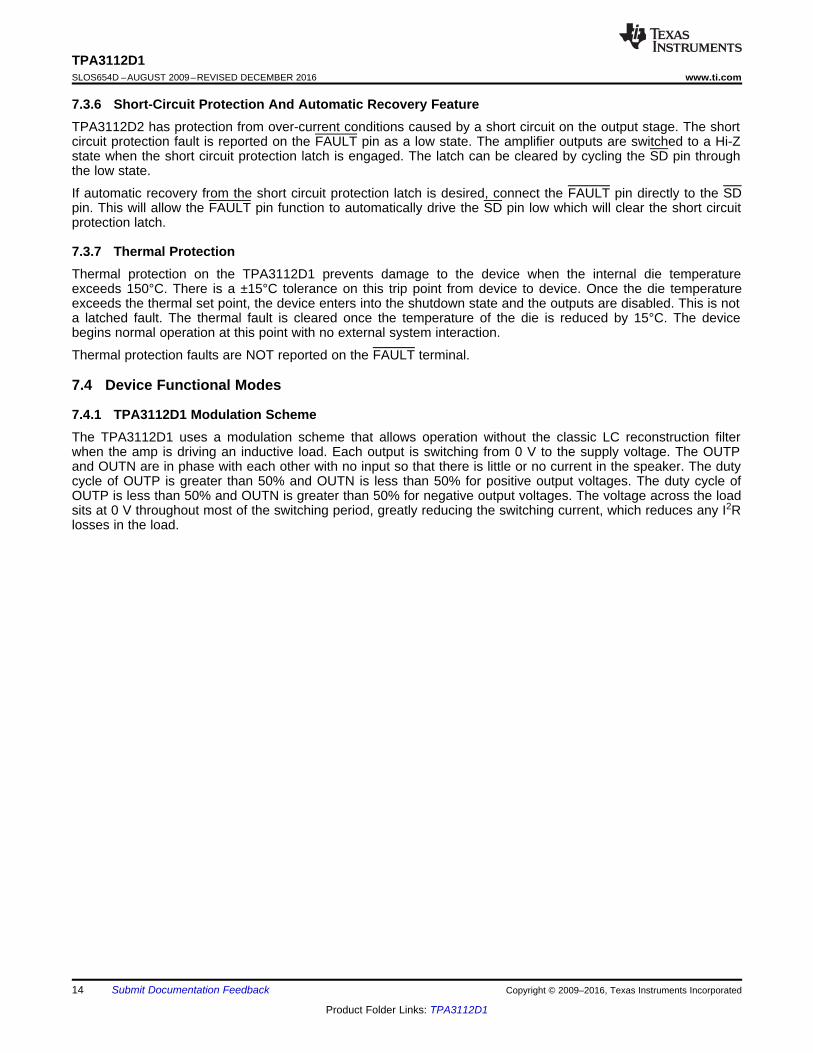
7.4.1 TPA3112D1 Modulation SchemeThe TPA3112D1 uses a modulation scheme that allows operation without the classic LC reconstruction filterwhen the amp is driving an inductive load. Each output is switching from 0 V to the supply voltage. The OUTPand OUTN are in phase with each other with no input so that there is little or no current in the speaker. The dutycycle of OUTP is greater than 50% and OUTN is less than 50% for positive output voltages. The duty cycle ofOUTP is less than 50% and OUTN is greater than 50% for negative output voltages. The voltage across the loadsits at 0 V throughout most of the switching period, greatly reducing the switching current, which reduces any I2Rlosses in the load.
0 V
-12 V
+12 V
Current
OUTP
OUTN
Differential
Voltage
Across
Load
0 V
-12 V
+12 V
Current
OUTP
OUTN
Differential
Voltage
Across
Load
Output = 0 V
Output > 0 V
15
TPA3112D1www.ti.com SLOS654D –AUGUST 2009–REVISED DECEMBER 2016
Product Folder Links: TPA3112D1
Submit Documentation FeedbackCopyright © 2009–2016, Texas Instruments Incorporated
Device Functional Modes (continued)
Figure 16. The TPA3112D1 Output Voltage and Current Waveforms into an Inductive Load
PVCC
PVCC
GAIN16
AVCC7
8AGND
9GVDD
OUTN
BSN
BSP
OUTP
23
22
21
20
TPA3112D1
FAULT2
GND3
4GND
5GAIN0
PVCC
BSN
OUTN
PGND
27
26
25
24
PLIMIT10
INN11
12INP
13NC
PGND
OUTP
BSP
PVCC
19
18
17
16
AVCC14
PVCC15
GND
29PowerPAD
SD1
PVCC28
PVCC
100 μF 0.1 μF
1000pF
100 Fμ 0.1 μF
1000pF
Audio
Source
Control
System
AVCC
100k Ω
10
100 kW
(1)
Ω
AVCC
1 kΩ
FB
FB
0.47 μF
1000 pF
0.47 μF
1000 pF
1 uF
1 uF
1 uF
1 uF
Copyright © 2016, Texas Instruments Incorporated
16
TPA3112D1SLOS654D –AUGUST 2009–REVISED DECEMBER 2016 www.ti.com
Product Folder Links: TPA3112D1
Submit Documentation Feedback Copyright © 2009–2016, Texas Instruments Incorporated
8 Application and Implementation
NOTEInformation in the following applications sections is not part of the TI componentspecification, and TI does not warrant its accuracy or completeness. TI’s customers areresponsible for determining suitability of components for their purposes. Customers shouldvalidate and test their design implementation to confirm system functionality.
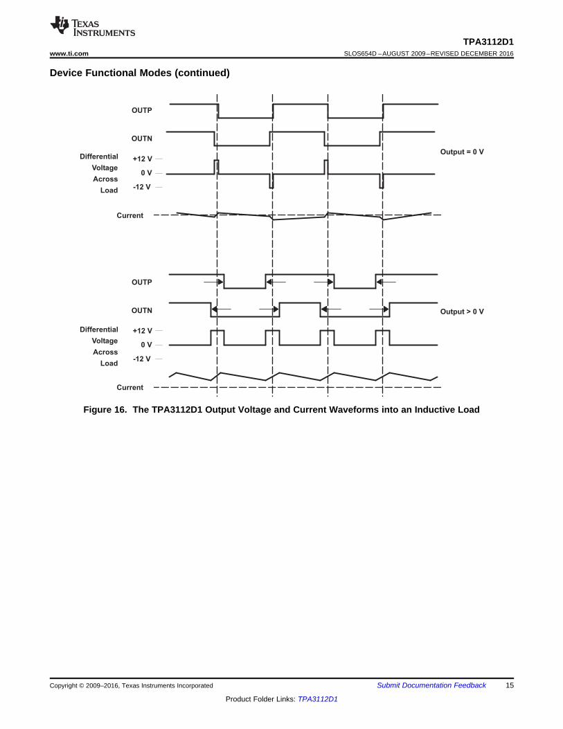
8.1 Application InformationThe TPA3112D1 is designed for use in stereo speakers like in televisions, monitors and laptops, and consumeraudio equipment. The TPA3112D1 can either be configured in stereo or mono mode, depending on output powerconditions. Depending on output power requirements and necessity for (speaker) load protection, the built-inPLIMIT circuit can be used to control system power.
8.2 Typical Application
(1) 100 kΩ resistor is needed if the PVCC slew rate is more than 10 V/ms.
Figure 17. Mono Class-D Amplifier With Btl Output
17
TPA3112D1www.ti.com SLOS654D –AUGUST 2009–REVISED DECEMBER 2016
Product Folder Links: TPA3112D1
Submit Documentation FeedbackCopyright © 2009–2016, Texas Instruments Incorporated
Typical Application (continued)8.2.1 Design RequirementsFor this design example, use the parameters listed in Table 4 as the input parameters.
Table 4. Design ParametersPARAMETER EXAMPLE VALUE
Input voltage range PVDD 8 V to 26 VFerrite bead + capacitor 120 Ω to 600 Ω at 100 MHz + 1 nF / 2.2 nF
8.2.2 Detailed Design Procedure
8.2.2.1 Ferrite Bead Filter ConsiderationsUsing the Advanced Emissions Suppression Technology in the TPA3112D1 amplifier it is possible to design ahigh efficiency Class-D audio amplifier while minimizing interference to surrounding circuits. it is also possible toaccomplish this with only a low-cost ferrite bead filter. In this case it is necessary to carefully select the ferritebead used in the filter.
One important aspect of the ferrite bead selection is the type of material used in the ferrite bead. Not all ferritematerial is alike, so it is important to select a material that is effective in the 10 to 100 MHz range which is key tothe operation of the Class D amplifier. Many of the specifications regulating consumer electronics haveemissions limits as low as 30 MHz. It is important to use the ferrite bead filter to block radiation in the 30 MHzand above range from appearing on the speaker wires and the power supply lines which are good antennas forthese signals. The impedance of the ferrite bead can be used along with a small capacitor with a value in therange of 1000 pF to reduce the frequency spectrum of the signal to an acceptable level. For best performance,the resonant frequency of the ferrite bead/ capacitor filter should be less than 10 MHz.
Also, it is important that the ferrite bead is large enough to maintain its impedance at the peak currents expectedfor the amplifier. Some ferrite bead manufacturers specify the bead impedance at a variety of current levels. Inthis case it is possible to make sure the ferrite bead maintains an adequate amount of impedance at the peakcurrent the amplifier will see. If these specifications are not available, it is also possible to estimate the beadcurrent handling capability by measuring the resonant frequency of the filter output at very low power and atmaximum power. A change of resonant frequency of less than fifty percent under this condition is desirable.Examples of ferrite beads which have been tested and work well with the TPA3112D2 include 28L0138-80R-10and HI1812V101R-10 from Steward and the 742792510 from Wurth Electronics.
A high-quality ceramic capacitor is also needed for the ferrite bead filter. A low ESR capacitor with goodtemperature and voltage characteristics will work best.
Additional EMC improvements may be obtained by adding snubber networks from each of the class D outputs toground. Suggested values for a simple RC series snubber network would be 10 Ω in series with a 330 pFcapacitor although design of the snubber network is specific to every application and must be designed takinginto account the parasitic reactance of the printed circuit board as well as the audio amp. Take care to evaluatethe stress on the component in the snubber network especially if the amp is running at high PVCC. Also, makesure the layout of the snubber network is tight and returns directly to the PGND or the PowerPAD™ beneath thechip.
8.2.2.2 Efficiency: LC Filter Required With the Traditional Class-D Modulation SchemeThe main reason that the traditional class-D amplifier needs an output filter is that the switching waveform resultsin maximum current flow. This causes more loss in the load, which causes lower efficiency. The ripple current islarge for the traditional modulation scheme, because the ripple current is proportional to voltage multiplied by thetime at that voltage. The differential voltage swing is 2 × VCC, and the time at each voltage is half the period forthe traditional modulation scheme. An ideal LC filter is needed to store the ripple current from each half cycle forthe next half cycle, while any resistance causes power dissipation. The speaker is both resistive and reactive,whereas an LC filter is almost purely reactive.
The TPA3112D1 modulation scheme has little loss in the load without a filter because the pulses are short andthe change in voltage is VCC instead of 2 × VCC. As the output power increases, the pulses widen, making theripple current larger. Ripple current could be filtered with an LC filter for increased efficiency, but for mostapplications the filter is not needed.
1 nF
Ferrite
Chip Bead
OUTP
OUTN
Ferrite
Chip Bead
1 nF
2.2 mF
15 Hm
15 mH
OUTP
OUTN
L1
L2
C2
C3
2.2 mF
1 mF
1 mF
33 Hm
33 mH
OUTP
OUTN
L1
L2
C2
C3
18
TPA3112D1SLOS654D –AUGUST 2009–REVISED DECEMBER 2016 www.ti.com
Product Folder Links: TPA3112D1
Submit Documentation Feedback Copyright © 2009–2016, Texas Instruments Incorporated
An LC filter with a cutoff frequency less than the class-D switching frequency allows the switching current to flowthrough the filter instead of the load. The filter has less resistance but higher impedance at the switchingfrequency than the speaker, which results in less power dissipation, therefore increasing efficiency.
8.2.2.3 When to Use an Output Filter for EMI SuppressionThe TPA3112D1 has been tested with a simple ferrite bead filter for a variety of applications including longspeaker wires up to 125 cm and high power. The TPA3112D1 EVM passes FCC Class B specifications underthese conditions using twisted speaker wires. The size and type of ferrite bead can be selected to meetapplication requirements. Also, the filter capacitor can be increased if necessary with some impact on efficiency.
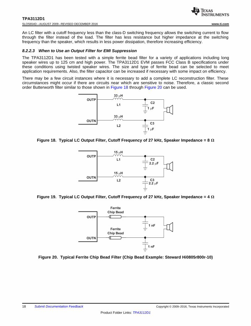
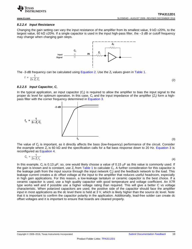
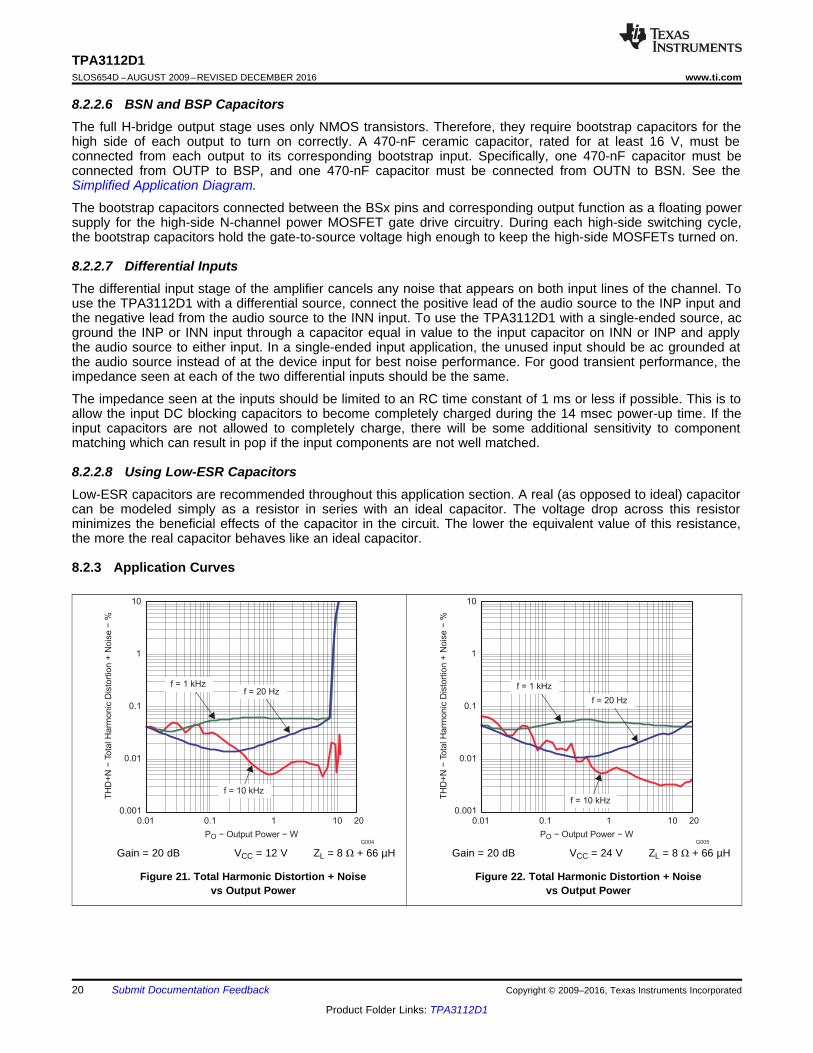
There may be a few circuit instances where it is necessary to add a complete LC reconstruction filter. Thesecircumstances might occur if there are circuits near which are sensitive to noise. Therefore, a classic secondorder Butterworth filter similar to those shown in Figure 18 through Figure 20 can be used.
Figure 18. Typical LC Output Filter, Cutoff Frequency of 27 kHz, Speaker Impedance = 8 Ω
Figure 19. Typical LC Output Filter, Cutoff Frequency of 27 kHz, Speaker Impedance = 4 Ω
Figure 20. Typical Ferrite Chip Bead Filter (Chip Bead Example: Steward Hi0805r800r-10)
C =i
1
2 Z fpi c
f =c
1
2 Z Cpi i
-3 dB
fc
f =1
2 Z Cpi i
Ci
INZi
Zf
Input
Signal
19
TPA3112D1www.ti.com SLOS654D –AUGUST 2009–REVISED DECEMBER 2016
Product Folder Links: TPA3112D1
Submit Documentation FeedbackCopyright © 2009–2016, Texas Instruments Incorporated
8.2.2.4 Input ResistanceChanging the gain setting can vary the input resistance of the amplifier from its smallest value, 9 kΩ ±20%, to thelargest value, 60 kΩ ±20%. If a single capacitor is used in the input high-pass filter, the –3 dB or cutoff frequencymay change when changing gain steps.
The -3-dB frequency can be calculated using Equation 2. Use the ZI values given in Table 1.
(2)
8.2.2.5 Input Capacitor, CI
In the typical application, an input capacitor (CI) is required to allow the amplifier to bias the input signal to theproper dc level for optimum operation. In this case, CI and the input impedance of the amplifier (ZI) form a high-pass filter with the corner frequency determined in Equation 3.
(3)
The value of CI is important, as it directly affects the bass (low-frequency) performance of the circuit. Considerthe example where ZI is 60 kΩ and the specification calls for a flat bass response down to 20 Hz. Equation 3 isreconfigured as Equation 4.
(4)
In this example, CI is 0.13 µF; so, one would likely choose a value of 0.15 μF as this value is commonly used. Ifthe gain is known and is constant, use ZI from Table 1 to calculate CI. A further consideration for this capacitor isthe leakage path from the input source through the input network CI) and the feedback network to the load. Thisleakage current creates a dc offset voltage at the input to the amplifier that reduces useful headroom, especiallyin high gain applications. For this reason, a low-leakage tantalum or ceramic capacitor is the best choice. If aceramic capacitor is used, use a high quality capacitor with good temperature and voltage coefficient. An X7Rtype works well and if possible use a higher voltage rating than required. This will give a better C vs voltagecharacteristic. When polarized capacitors are used, the positive side of the capacitor should face the amplifierinput in most applications as the dc level there is held at 3 V, which is likely higher than the source dc level. Notethat it is important to confirm the capacitor polarity in the application. Additionally, lead-free solder can create dcoffset voltages and it is important to ensure that boards are cleaned properly.
PO − Output Power − W
0.01 0.1 1 10
TH
D+
N−
Tota
l H
arm
onic
Dis
tort
ion +
Nois
e−
%
0.001
0.1
10
20
0.01
1
G004
f = 1 kHzf = 20 Hz
f = 10 kHz
PO − Output Power − W
TH
D+
N−
Tota
l H
arm
onic
Dis
tort
ion +
Nois
e−
%
0.001
0.1
10
0.01
1
G005
f = 1 kHz
f = 20 Hz
f = 10 kHz
0.01 0.1 1 10 20
20
TPA3112D1SLOS654D –AUGUST 2009–REVISED DECEMBER 2016 www.ti.com
Product Folder Links: TPA3112D1
Submit Documentation Feedback Copyright © 2009–2016, Texas Instruments Incorporated
8.2.2.6 BSN and BSP CapacitorsThe full H-bridge output stage uses only NMOS transistors. Therefore, they require bootstrap capacitors for thehigh side of each output to turn on correctly. A 470-nF ceramic capacitor, rated for at least 16 V, must beconnected from each output to its corresponding bootstrap input. Specifically, one 470-nF capacitor must beconnected from OUTP to BSP, and one 470-nF capacitor must be connected from OUTN to BSN. See theSimplified Application Diagram.
The bootstrap capacitors connected between the BSx pins and corresponding output function as a floating powersupply for the high-side N-channel power MOSFET gate drive circuitry. During each high-side switching cycle,the bootstrap capacitors hold the gate-to-source voltage high enough to keep the high-side MOSFETs turned on.
8.2.2.7 Differential InputsThe differential input stage of the amplifier cancels any noise that appears on both input lines of the channel. Touse the TPA3112D1 with a differential source, connect the positive lead of the audio source to the INP input andthe negative lead from the audio source to the INN input. To use the TPA3112D1 with a single-ended source, acground the INP or INN input through a capacitor equal in value to the input capacitor on INN or INP and applythe audio source to either input. In a single-ended input application, the unused input should be ac grounded atthe audio source instead of at the device input for best noise performance. For good transient performance, theimpedance seen at each of the two differential inputs should be the same.
The impedance seen at the inputs should be limited to an RC time constant of 1 ms or less if possible. This is toallow the input DC blocking capacitors to become completely charged during the 14 msec power-up time. If theinput capacitors are not allowed to completely charge, there will be some additional sensitivity to componentmatching which can result in pop if the input components are not well matched.
8.2.2.8 Using Low-ESR CapacitorsLow-ESR capacitors are recommended throughout this application section. A real (as opposed to ideal) capacitorcan be modeled simply as a resistor in series with an ideal capacitor. The voltage drop across this resistorminimizes the beneficial effects of the capacitor in the circuit. The lower the equivalent value of this resistance,the more the real capacitor behaves like an ideal capacitor.
8.2.3 Application Curves
Gain = 20 dB VCC = 12 V ZL = 8 Ω + 66 µH
Figure 21. Total Harmonic Distortion + Noisevs Output Power
Gain = 20 dB VCC = 24 V ZL = 8 Ω + 66 µH
Figure 22. Total Harmonic Distortion + Noisevs Output Power
0.01 0.1 1 10 20
PO − Output Power − W
TH
D+
N−
Tota
l H
arm
onic
Dis
tort
ion +
Nois
e−
%
0.001
0.1
10
0.01
1
G006
f = 1 kHz f = 20 Hz
f = 10 kHz
21
TPA3112D1www.ti.com SLOS654D –AUGUST 2009–REVISED DECEMBER 2016
Product Folder Links: TPA3112D1
Submit Documentation FeedbackCopyright © 2009–2016, Texas Instruments Incorporated
Gain = 20 dB VCC = 12 V ZL = 4 Ω + 33 µH
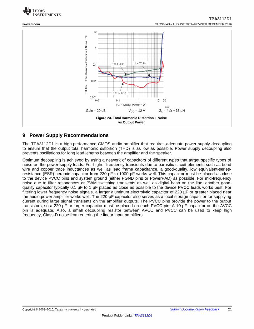
Figure 23. Total Harmonic Distortion + Noisevs Output Power
9 Power Supply RecommendationsThe TPA3112D1 is a high-performance CMOS audio amplifier that requires adequate power supply decouplingto ensure that the output total harmonic distortion (THD) is as low as possible. Power supply decoupling alsoprevents oscillations for long lead lengths between the amplifier and the speaker.
Optimum decoupling is achieved by using a network of capacitors of different types that target specific types ofnoise on the power supply leads. For higher frequency transients due to parasitic circuit elements such as bondwire and copper trace inductances as well as lead frame capacitance, a good-quality, low equivalent-series-resistance (ESR) ceramic capacitor from 220 pF to 1000 pF works well. This capacitor must be placed as closeto the device PVCC pins and system ground (either PGND pins or PowerPAD) as possible. For mid-frequencynoise due to filter resonances or PWM switching transients as well as digital hash on the line, another good-quality capacitor typically 0.1 µF to 1 µF placed as close as possible to the device PVCC leads works best. Forfiltering lower frequency noise signals, a larger aluminum electrolytic capacitor of 220 µF or greater placed nearthe audio power amplifier works well. The 220-µF capacitor also serves as a local storage capacitor for supplyingcurrent during large signal transients on the amplifier outputs. The PVCC pins provide the power to the outputtransistors, so a 220-µF or larger capacitor must be placed on each PVCC pin. A 10-µF capacitor on the AVCCpin is adequate. Also, a small decoupling resistor between AVCC and PVCC can be used to keep highfrequency, Class-D noise from entering the linear input amplifiers.
22
TPA3112D1SLOS654D –AUGUST 2009–REVISED DECEMBER 2016 www.ti.com
Product Folder Links: TPA3112D1
Submit Documentation Feedback Copyright © 2009–2016, Texas Instruments Incorporated
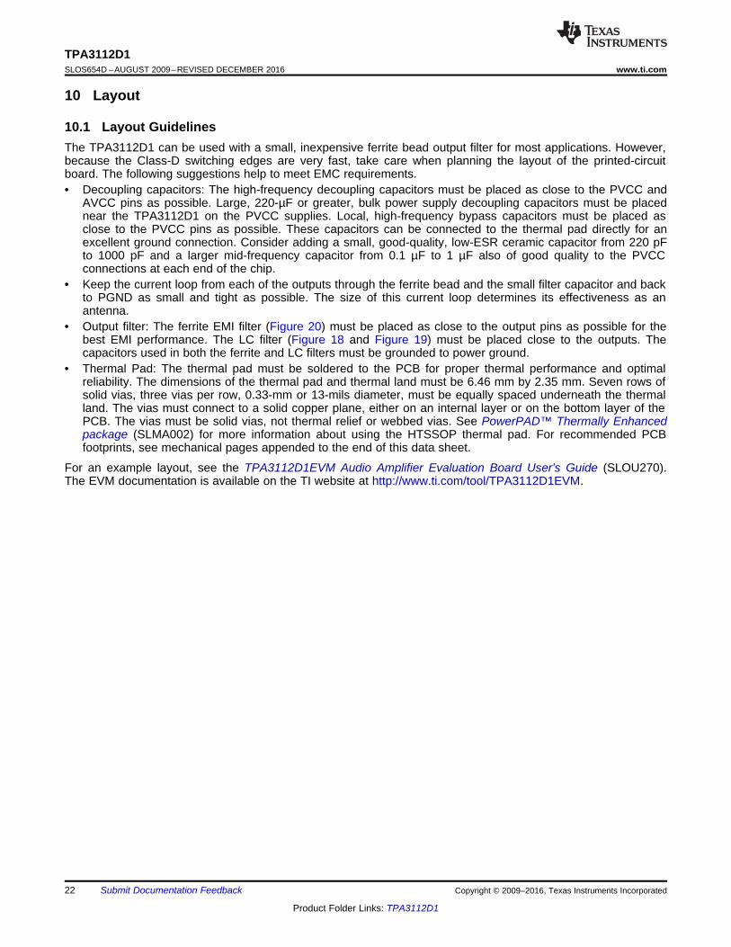
10 Layout
10.1 Layout GuidelinesThe TPA3112D1 can be used with a small, inexpensive ferrite bead output filter for most applications. However,because the Class-D switching edges are very fast, take care when planning the layout of the printed-circuitboard. The following suggestions help to meet EMC requirements.• Decoupling capacitors: The high-frequency decoupling capacitors must be placed as close to the PVCC and
AVCC pins as possible. Large, 220-µF or greater, bulk power supply decoupling capacitors must be placednear the TPA3112D1 on the PVCC supplies. Local, high-frequency bypass capacitors must be placed asclose to the PVCC pins as possible. These capacitors can be connected to the thermal pad directly for anexcellent ground connection. Consider adding a small, good-quality, low-ESR ceramic capacitor from 220 pFto 1000 pF and a larger mid-frequency capacitor from 0.1 µF to 1 µF also of good quality to the PVCCconnections at each end of the chip.
• Keep the current loop from each of the outputs through the ferrite bead and the small filter capacitor and backto PGND as small and tight as possible. The size of this current loop determines its effectiveness as anantenna.
• Output filter: The ferrite EMI filter (Figure 20) must be placed as close to the output pins as possible for thebest EMI performance. The LC filter (Figure 18 and Figure 19) must be placed close to the outputs. Thecapacitors used in both the ferrite and LC filters must be grounded to power ground.
• Thermal Pad: The thermal pad must be soldered to the PCB for proper thermal performance and optimalreliability. The dimensions of the thermal pad and thermal land must be 6.46 mm by 2.35 mm. Seven rows ofsolid vias, three vias per row, 0.33-mm or 13-mils diameter, must be equally spaced underneath the thermalland. The vias must connect to a solid copper plane, either on an internal layer or on the bottom layer of thePCB. The vias must be solid vias, not thermal relief or webbed vias. See PowerPAD™ Thermally Enhancedpackage (SLMA002) for more information about using the HTSSOP thermal pad. For recommended PCBfootprints, see mechanical pages appended to the end of this data sheet.
For an example layout, see the TPA3112D1EVM Audio Amplifier Evaluation Board User's Guide (SLOU270).The EVM documentation is available on the TI website at http://www.ti.com/tool/TPA3112D1EVM.
1nF
13
11
12
9
10
7
8
5
6
1
16
15
18
17
20
19
22
21
24
23
26
28
27
Top Layer Ground and Thermal Pad
Top Layer Signal Traces
Via to Bottom Ground Plane
Pad to Top Layer Ground Pour
3
4
2
25
1nF
14
100PF
100PF100nF
100nF
FB
1nF
1nF
1PF
1PF
FB
0.47µF
0.47µF
23
TPA3112D1www.ti.com SLOS654D –AUGUST 2009–REVISED DECEMBER 2016
Product Folder Links: TPA3112D1
Submit Documentation FeedbackCopyright © 2009–2016, Texas Instruments Incorporated
10.2 Layout Example
Figure 24. BTL Layout Example
24
TPA3112D1SLOS654D –AUGUST 2009–REVISED DECEMBER 2016 www.ti.com
Product Folder Links: TPA3112D1
Submit Documentation Feedback Copyright © 2009–2016, Texas Instruments Incorporated
11 Device and Documentation Support
11.1 Device Support
11.1.1 Development SupportFor development support, see the following:
The TI PCB Thermal Calculator is designed to estimate the junction temperatures of components which useexposed-pad packages.
11.2 Documentation Support
11.2.1 Related DocumentationFor related documentation see the following:• Quad Flatpack No-Lead Logic Packages (SCBA017)• QFN/SON PCB Attachment (SLUA271)• PowerPAD™ Thermally Enhanced package (SLMA002)• TPA3112D1EVM Audio Amplifier Evaluation Board User's Guide (SLOU270)
11.3 Recieving Notification of Documentation UpdatesTo receive notification of documentation updates, navigate to the device product folder on ti.com. In the upperright corner, click on Alert me to register and receive a weekly digest of any product information that haschanged. For change details, review the revision history included in any revised document.
11.4 Community ResourcesThe following links connect to TI community resources. Linked contents are provided "AS IS" by the respectivecontributors. They do not constitute TI specifications and do not necessarily reflect TI's views; see TI's Terms ofUse.
TI E2E™ Online Community TI's Engineer-to-Engineer (E2E) Community. Created to foster collaborationamong engineers. At e2e.ti.com, you can ask questions, share knowledge, explore ideas and helpsolve problems with fellow engineers.
Design Support TI's Design Support Quickly find helpful E2E forums along with design support tools andcontact information for technical support.
11.5 TrademarksSpeakerGuard, PowerPAD, E2E are trademarks of Texas Instruments.All other trademarks are the property of their respective owners.
11.6 Electrostatic Discharge CautionThese devices have limited built-in ESD protection. The leads should be shorted together or the device placed in conductive foamduring storage or handling to prevent electrostatic damage to the MOS gates.
11.7 GlossarySLYZ022 — TI Glossary.
This glossary lists and explains terms, acronyms, and definitions.
25
TPA3112D1www.ti.com SLOS654D –AUGUST 2009–REVISED DECEMBER 2016
Product Folder Links: TPA3112D1
Submit Documentation FeedbackCopyright © 2009–2016, Texas Instruments Incorporated
12 Mechanical, Packaging, and Orderable InformationThe following pages include mechanical, packaging, and orderable information. This information is the mostcurrent data available for the designated devices. This data is subject to change without notice and revision ofthis document. For browser-based versions of this data sheet, refer to the left-hand navigation.
PACKAGE OPTION ADDENDUM
www.ti.com 1-Mar-2016
Addendum-Page 1
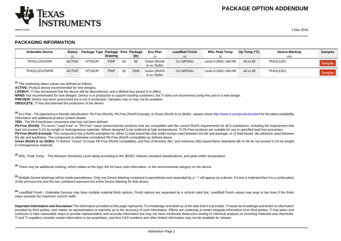
PACKAGING INFORMATION
Orderable Device Status(1)
Package Type PackageDrawing
Pins PackageQty
Eco Plan(2)
Lead/Ball Finish(6)
MSL Peak Temp(3)
Op Temp (°C) Device Marking(4/5)
Samples
TPA3112D1PWP ACTIVE HTSSOP PWP 28 50 Green (RoHS& no Sb/Br)
CU NIPDAU Level-3-260C-168 HR -40 to 85 TPA3112D1
TPA3112D1PWPR ACTIVE HTSSOP PWP 28 2000 Green (RoHS& no Sb/Br)
CU NIPDAU Level-3-260C-168 HR -40 to 85 TPA3112D1
(1) The marketing status values are defined as follows:ACTIVE: Product device recommended for new designs.LIFEBUY: TI has announced that the device will be discontinued, and a lifetime-buy period is in effect.NRND: Not recommended for new designs. Device is in production to support existing customers, but TI does not recommend using this part in a new design.PREVIEW: Device has been announced but is not in production. Samples may or may not be available.OBSOLETE: TI has discontinued the production of the device.
(2) Eco Plan - The planned eco-friendly classification: Pb-Free (RoHS), Pb-Free (RoHS Exempt), or Green (RoHS & no Sb/Br) - please check http://www.ti.com/productcontent for the latest availabilityinformation and additional product content details.TBD: The Pb-Free/Green conversion plan has not been defined.Pb-Free (RoHS): TI's terms "Lead-Free" or "Pb-Free" mean semiconductor products that are compatible with the current RoHS requirements for all 6 substances, including the requirement thatlead not exceed 0.1% by weight in homogeneous materials. Where designed to be soldered at high temperatures, TI Pb-Free products are suitable for use in specified lead-free processes.Pb-Free (RoHS Exempt): This component has a RoHS exemption for either 1) lead-based flip-chip solder bumps used between the die and package, or 2) lead-based die adhesive used betweenthe die and leadframe. The component is otherwise considered Pb-Free (RoHS compatible) as defined above.Green (RoHS & no Sb/Br): TI defines "Green" to mean Pb-Free (RoHS compatible), and free of Bromine (Br) and Antimony (Sb) based flame retardants (Br or Sb do not exceed 0.1% by weightin homogeneous material)
(3) MSL, Peak Temp. - The Moisture Sensitivity Level rating according to the JEDEC industry standard classifications, and peak solder temperature.
(4) There may be additional marking, which relates to the logo, the lot trace code information, or the environmental category on the device.
(5) Multiple Device Markings will be inside parentheses. Only one Device Marking contained in parentheses and separated by a "~" will appear on a device. If a line is indented then it is a continuationof the previous line and the two combined represent the entire Device Marking for that device.
(6) Lead/Ball Finish - Orderable Devices may have multiple material finish options. Finish options are separated by a vertical ruled line. Lead/Ball Finish values may wrap to two lines if the finishvalue exceeds the maximum column width.
Important Information and Disclaimer:The information provided on this page represents TI's knowledge and belief as of the date that it is provided. TI bases its knowledge and belief on informationprovided by third parties, and makes no representation or warranty as to the accuracy of such information. Efforts are underway to better integrate information from third parties. TI has taken andcontinues to take reasonable steps to provide representative and accurate information but may not have conducted destructive testing or chemical analysis on incoming materials and chemicals.TI and TI suppliers consider certain information to be proprietary, and thus CAS numbers and other limited information may not be available for release.
PACKAGE OPTION ADDENDUM
www.ti.com 1-Mar-2016
Addendum-Page 2
In no event shall TI's liability arising out of such information exceed the total purchase price of the TI part(s) at issue in this document sold by TI to Customer on an annual basis.
OTHER QUALIFIED VERSIONS OF TPA3112D1 :
• Automotive: TPA3112D1-Q1
NOTE: Qualified Version Definitions:
• Automotive - Q100 devices qualified for high-reliability automotive applications targeting zero defects
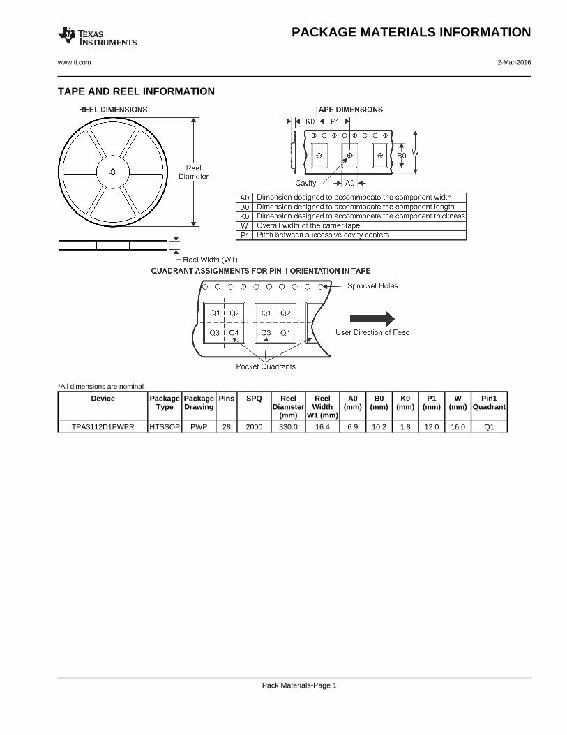
TAPE AND REEL INFORMATION
*All dimensions are nominal
Device PackageType
PackageDrawing
Pins SPQ ReelDiameter
(mm)
ReelWidth
W1 (mm)
A0(mm)
B0(mm)
K0(mm)
P1(mm)
W(mm)
Pin1Quadrant
TPA3112D1PWPR HTSSOP PWP 28 2000 330.0 16.4 6.9 10.2 1.8 12.0 16.0 Q1
PACKAGE MATERIALS INFORMATION
www.ti.com 2-Mar-2016
Pack Materials-Page 1
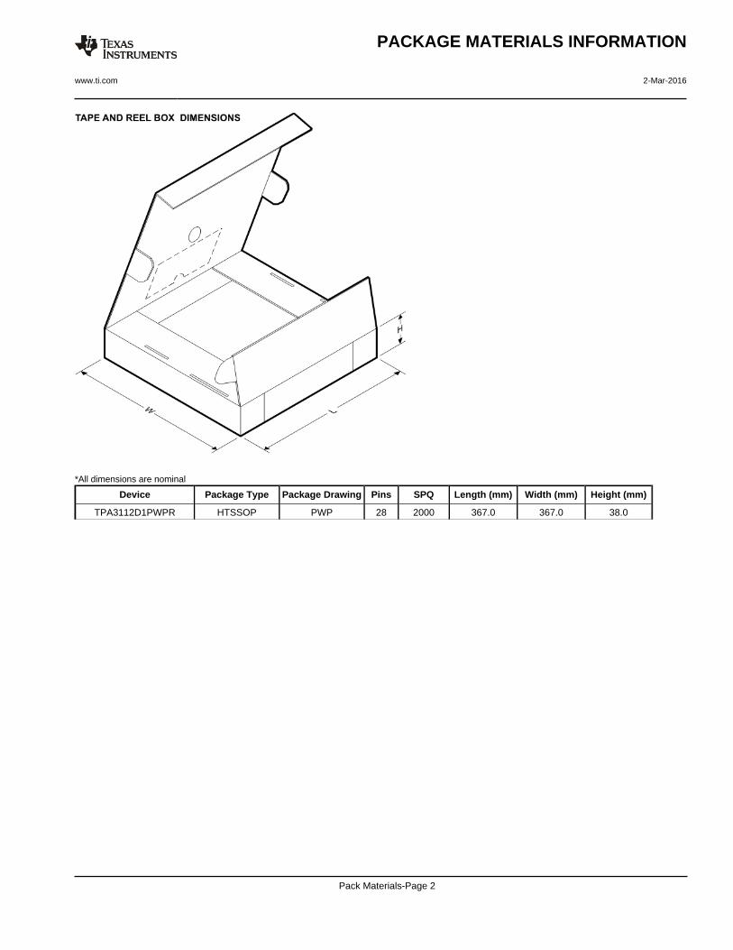
*All dimensions are nominal
Device Package Type Package Drawing Pins SPQ Length (mm) Width (mm) Height (mm)
TPA3112D1PWPR HTSSOP PWP 28 2000 367.0 367.0 38.0
PACKAGE MATERIALS INFORMATION
www.ti.com 2-Mar-2016
Pack Materials-Page 2
IMPORTANT NOTICE
Texas Instruments Incorporated and its subsidiaries (TI) reserve the right to make corrections, enhancements, improvements and otherchanges to its semiconductor products and services per JESD46, latest issue, and to discontinue any product or service per JESD48, latestissue. Buyers should obtain the latest relevant information before placing orders and should verify that such information is current andcomplete. All semiconductor products (also referred to herein as “components”) are sold subject to TI’s terms and conditions of salesupplied at the time of order acknowledgment.TI warrants performance of its components to the specifications applicable at the time of sale, in accordance with the warranty in TI’s termsand conditions of sale of semiconductor products. Testing and other quality control techniques are used to the extent TI deems necessaryto support this warranty. Except where mandated by applicable law, testing of all parameters of each component is not necessarilyperformed.TI assumes no liability for applications assistance or the design of Buyers’ products. Buyers are responsible for their products andapplications using TI components. To minimize the risks associated with Buyers’ products and applications, Buyers should provideadequate design and operating safeguards.TI does not warrant or represent that any license, either express or implied, is granted under any patent right, copyright, mask work right, orother intellectual property right relating to any combination, machine, or process in which TI components or services are used. Informationpublished by TI regarding third-party products or services does not constitute a license to use such products or services or a warranty orendorsement thereof. Use of such information may require a license from a third party under the patents or other intellectual property of thethird party, or a license from TI under the patents or other intellectual property of TI.Reproduction of significant portions of TI information in TI data books or data sheets is permissible only if reproduction is without alterationand is accompanied by all associated warranties, conditions, limitations, and notices. TI is not responsible or liable for such altereddocumentation. Information of third parties may be subject to additional restrictions.Resale of TI components or services with statements different from or beyond the parameters stated by TI for that component or servicevoids all express and any implied warranties for the associated TI component or service and is an unfair and deceptive business practice.TI is not responsible or liable for any such statements.Buyer acknowledges and agrees that it is solely responsible for compliance with all legal, regulatory and safety-related requirementsconcerning its products, and any use of TI components in its applications, notwithstanding any applications-related information or supportthat may be provided by TI. Buyer represents and agrees that it has all the necessary expertise to create and implement safeguards whichanticipate dangerous consequences of failures, monitor failures and their consequences, lessen the likelihood of failures that might causeharm and take appropriate remedial actions. Buyer will fully indemnify TI and its representatives against any damages arising out of the useof any TI components in safety-critical applications.In some cases, TI components may be promoted specifically to facilitate safety-related applications. With such components, TI’s goal is tohelp enable customers to design and create their own end-product solutions that meet applicable functional safety standards andrequirements. Nonetheless, such components are subject to these terms.No TI components are authorized for use in FDA Class III (or similar life-critical medical equipment) unless authorized officers of the partieshave executed a special agreement specifically governing such use.Only those TI components which TI has specifically designated as military grade or “enhanced plastic” are designed and intended for use inmilitary/aerospace applications or environments. Buyer acknowledges and agrees that any military or aerospace use of TI componentswhich have not been so designated is solely at the Buyer's risk, and that Buyer is solely responsible for compliance with all legal andregulatory requirements in connection with such use.TI has specifically designated certain components as meeting ISO/TS16949 requirements, mainly for automotive use. In any case of use ofnon-designated products, TI will not be responsible for any failure to meet ISO/TS16949.
Products ApplicationsAudio www.ti.com/audio Automotive and Transportation www.ti.com/automotiveAmplifiers amplifier.ti.com Communications and Telecom www.ti.com/communicationsData Converters dataconverter.ti.com Computers and Peripherals www.ti.com/computersDLP® Products www.dlp.com Consumer Electronics www.ti.com/consumer-appsDSP dsp.ti.com Energy and Lighting www.ti.com/energyClocks and Timers www.ti.com/clocks Industrial www.ti.com/industrialInterface interface.ti.com Medical www.ti.com/medicalLogic logic.ti.com Security www.ti.com/securityPower Mgmt power.ti.com Space, Avionics and Defense www.ti.com/space-avionics-defenseMicrocontrollers microcontroller.ti.com Video and Imaging www.ti.com/videoRFID www.ti-rfid.comOMAP Applications Processors www.ti.com/omap TI E2E Community e2e.ti.comWireless Connectivity www.ti.com/wirelessconnectivity
Mailing Address: Texas Instruments, Post Office Box 655303, Dallas, Texas 75265Copyright © 2016, Texas Instruments Incorporated