CC Obsolete Product(s) - Obsolete Product(s) · For each SPI transfer, ... VRin/VLin Maximum Rin &...
28
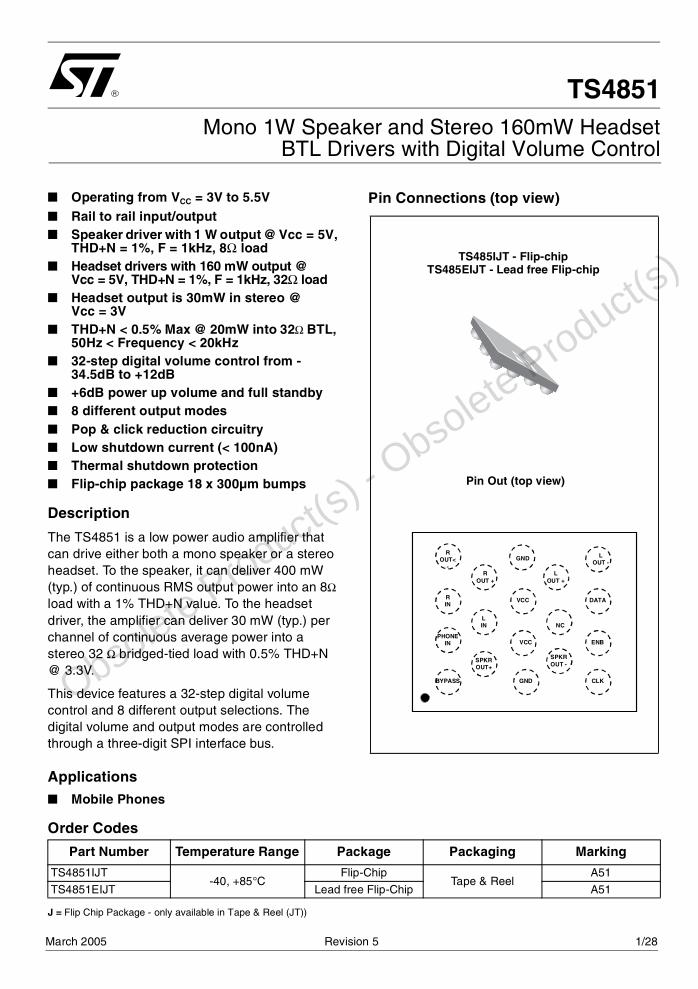
March 2005 Revision 5 1/28 ■ Operating from V CC = 3V to 5.5V ■ Rail to rail input/output ■ Speaker driver with 1 W output @ Vcc = 5V, THD+N = 1%, F = 1kHz, 8Ω load ■ Headset drivers with 160 mW output @ Vcc = 5V, THD+N = 1%, F = 1kHz, 32Ω load ■ Headset output is 30mW in stereo @ Vcc = 3V ■ THD+N < 0.5% Max @ 20mW into 32Ω BTL, 50Hz < Frequency < 20kHz ■ 32-step digital volume control from - 34.5dB to +12dB ■ +6dB power up volume and full standby ■ 8 different output modes ■ Pop & click reduction circuitry ■ Low shutdown current (< 100nA) ■ Thermal shutdown protection ■ Flip-chip package 18 x 300μm bumps Description The TS4851 is a low power audio amplifier that can drive either both a mono speaker or a stereo headset. To the speaker, it can deliver 400 mW (typ.) of continuous RMS output power into an 8Ω load with a 1% THD+N value. To the headset driver, the amplifier can deliver 30 mW (typ.) per channel of continuous average power into a stereo 32 Ω bridged-tied load with 0.5% THD+N @ 3.3V. This device features a 32-step digital volume control and 8 different output selections. The digital volume and output modes are controlled through a three-digit SPI interface bus. Pin Connections (top view) Applications ■ Mobile Phones Order Codes J = Flip Chip Package - only available in Tape & Reel (JT)) Pin Out (top view) TS485IJT - Flip-chip TS485EIJT - Lead free Flip-chip BYPASS R OUT< - R OUT + GND L OUT + L OUT - R IN L IN VCC DATA VCC NC PHONE IN SPKR OUT+ SPKR OUT - ENB GND CLK Part Number Temperature Range Package Packaging Marking TS4851IJT -40, +85°C Flip-Chip Tape & Reel A51 TS4851EIJT Lead free Flip-Chip A51 TS4851 Mono 1W Speaker and Stereo 160mW Headset BTL Drivers with Digital Volume Control Obsolete Product(s) - Obsolete Product(s)
Transcript of CC Obsolete Product(s) - Obsolete Product(s) · For each SPI transfer, ... VRin/VLin Maximum Rin &...
TS4851Mono 1W Speaker and Stereo 160mW Headset
BTL Drivers with Digital Volume Control
Operating from VCC = 3V to 5.5V Rail to rail input/output Speaker driver with 1 W output @ Vcc = 5V,
THD+N = 1%, F = 1kHz, 8Ω load Headset drivers with 160 mW output @
Vcc = 5V, THD+N = 1%, F = 1kHz, 32Ω load Headset output is 30mW in stereo @
Vcc = 3V THD+N < 0.5% Max @ 20mW into 32Ω BTL,
50Hz < Frequency < 20kHz 32-step digital volume control from -
34.5dB to +12dB +6dB power up volume and full standby 8 different output modes Pop & click reduction circuitry Low shutdown current (< 100nA) Thermal shutdown protection Flip-chip package 18 x 300µm bumps
Description
The TS4851 is a low power audio amplifier that can drive either both a mono speaker or a stereo headset. To the speaker, it can deliver 400 mW (typ.) of continuous RMS output power into an 8Ω load with a 1% THD+N value. To the headset driver, the amplifier can deliver 30 mW (typ.) per channel of continuous average power into a stereo 32 Ω bridged-tied load with 0.5% THD+N @ 3.3V.
This device features a 32-step digital volume control and 8 different output selections. The digital volume and output modes are controlled through a three-digit SPI interface bus.
Pin Connections (top view)
Applications
Mobile Phones
Order Codes
J = Flip Chip Package - only available in Tape & Reel (JT))
Pin Out (top view)
TS485IJT - Flip-chipTS485EIJT - Lead free Flip-chip
BYPASS
ROUT<
-R
OUT +
GND
LOUT +
LOUT -
RIN
LIN
VCC DATA
VCC
NC
PHONEIN
SPKROUT+
SPKROUT -
ENB
GND CLKBYPASS
ROUT<
-R
OUT +
GND
LOUT +
LOUT -
RIN
LIN
VCC DATA
VCC
NC
PHONEIN
SPKROUT+
SPKROUT -
ENB
GND CLK
Part Number Temperature Range Package Packaging Marking
TS4851IJT-40, +85°C
Flip-ChipTape & Reel
A51
TS4851EIJT Lead free Flip-Chip A51
Obso
lete Product(s)
- Obso
lete Product(s)
March 2005 Revision 5 1/28
TS4851 Application Information
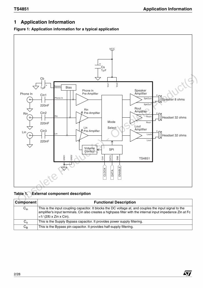
1 Application Information Figure 1: Application information for a typical application
Table 1. External component description
Component Functional Description
Cin This is the input coupling capacitor. It blocks the DC voltage at, and couples the input signal to the amplifier’s input terminals. Cin also creates a highpass filter with the internal input impedance Zin at Fc =1/ (2πi x Zin x Cin).
Cs This is the Supply Bypass capacitor. It provides power supply filtering.
CB This is the Bypass pin capacitor. It provides half-supply filtering.
Obso
lete Product(s)
- Obso
lete Product(s)
2/28
SPI Bus Interface TS4851
3/28
2 SPI Bus Interface
2.1 Description of SPI operation
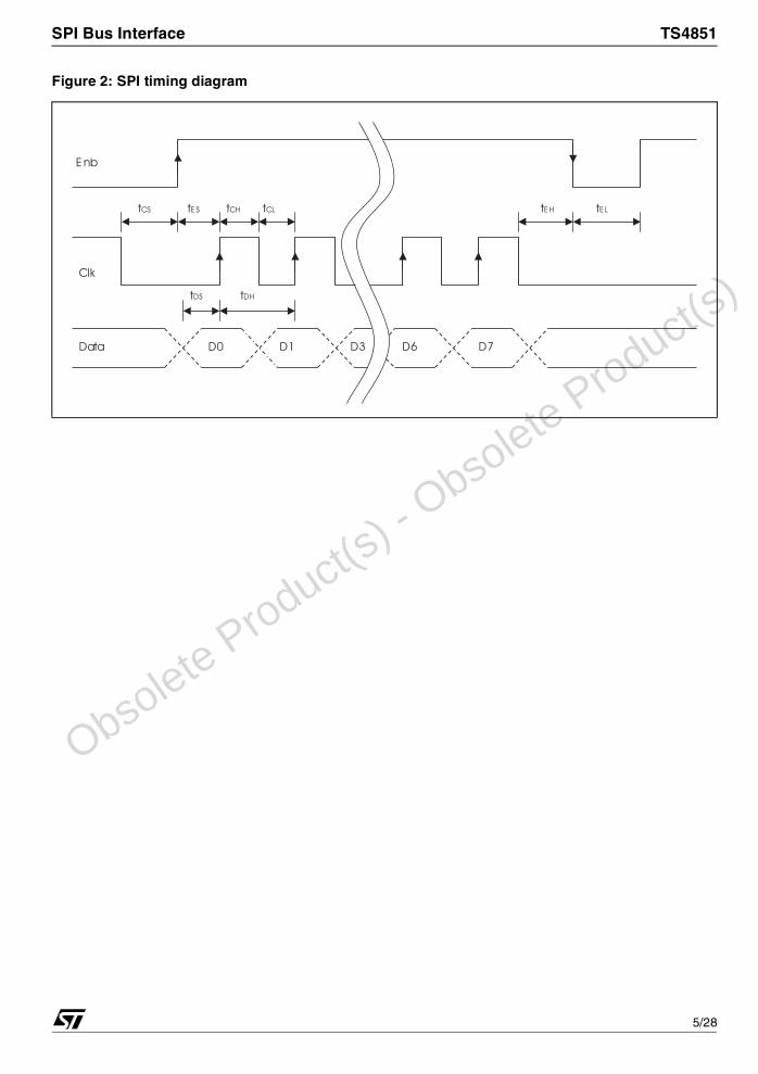
The serial data bits are organized into a field containing 8 bits of data as shown in Table 3. The DATA 0 to DATA 2 bits determine the output mode of the TS4851 as shown in Table 2. The DATA 3 to DATA 7 bits determine the gain level setting as illustrated by Table 3. For each SPI transfer, the data bits are written to the DATA pin with the least significant bit (LSB) first. All serial data are sampled at the rising edge of the CLK signal. Once all the data bits have been sampled, ENB transitions from logic-high to logic low to complete the SPI sequence. All 8 bits must be received before any data latch can occur. Any excess CLK and DATA transitions will be ignored after the height rising clock edge has occurred. For any data sequence longer than 8 bits, only the first 8 bits will get loaded into the shift register and the rest of the bits will be disregarded.
Table 2. Pin description
Pin Functional Description
DATA This is the serial data input pin. CLK This is the clock input pin.ENB This is the SPI enable pin active at high level.
Table 3. Bit allocation
DATA MODES
LSB DATA 0 Mode 1DATA 1 Mode 2DATA 2 Mode 3DATA 3 gain 1DATA 4 gain 2DATA 5 gain 3DATA 6 gain 4
MSB DATA 7 gain 5
Table 4. Output mode selection: G from -34.5dB to +12dB (by steps of 1.5dB)
Output Mode # DATA 2 DATA 1 DATA 0 SPKERout1
1) SD = Shutdown Mode, P = Phone in Input, R = Rin input and L = Lin input
Rout Lout
0 0 0 0 SD SD SD1 0 0 1 6dBxP SD SD2 0 1 0 SD 0dBxP 0dBxP3 0 1 1 Gx(R+L) SD SD4 1 0 0 SD GxR GxL5 1 0 1 Gx(R+L)
+6dBxP
SD SD
6 1 1 0 SD GxR+0dBxP GxL+0dBxP7 1 1 1 6dBxP GxR+0dBxP GxL+0dBxP
Obso
lete Product(s)
- Obso
lete Product(s)
TS4851 SPI Bus Interface
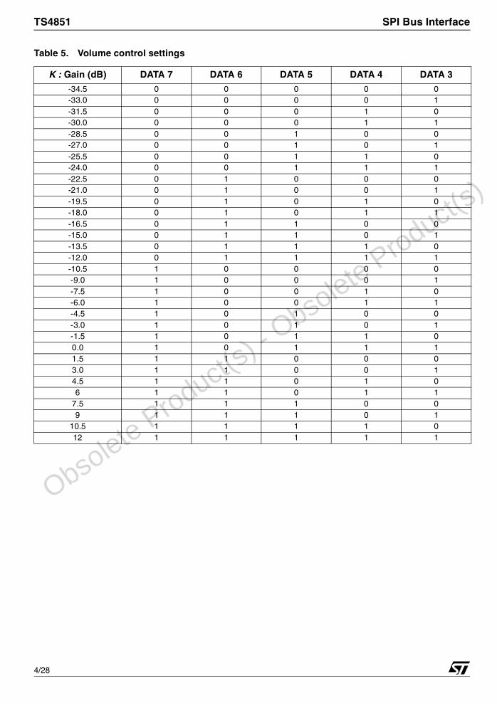
Table 5. Volume control settings
K : Gain (dB) DATA 7 DATA 6 DATA 5 DATA 4 DATA 3
-34.5 0 0 0 0 0-33.0 0 0 0 0 1-31.5 0 0 0 1 0-30.0 0 0 0 1 1-28.5 0 0 1 0 0-27.0 0 0 1 0 1-25.5 0 0 1 1 0-24.0 0 0 1 1 1-22.5 0 1 0 0 0-21.0 0 1 0 0 1-19.5 0 1 0 1 0-18.0 0 1 0 1 1-16.5 0 1 1 0 0-15.0 0 1 1 0 1-13.5 0 1 1 1 0-12.0 0 1 1 1 1-10.5 1 0 0 0 0-9.0 1 0 0 0 1-7.5 1 0 0 1 0-6.0 1 0 0 1 1-4.5 1 0 1 0 0-3.0 1 0 1 0 1-1.5 1 0 1 1 00.0 1 0 1 1 11.5 1 1 0 0 03.0 1 1 0 0 14.5 1 1 0 1 06 1 1 0 1 1
7.5 1 1 1 0 09 1 1 1 0 1
10.5 1 1 1 1 012 1 1 1 1 1
Obso
lete Product(s)
- Obso
lete Product(s)
4/28
SPI Bus Interface TS4851
Figure 2: SPI timing diagram
Obso
lete Product(s)
- Obso
lete Product(s)
5/28
TS4851 Absolute Maximum Ratings
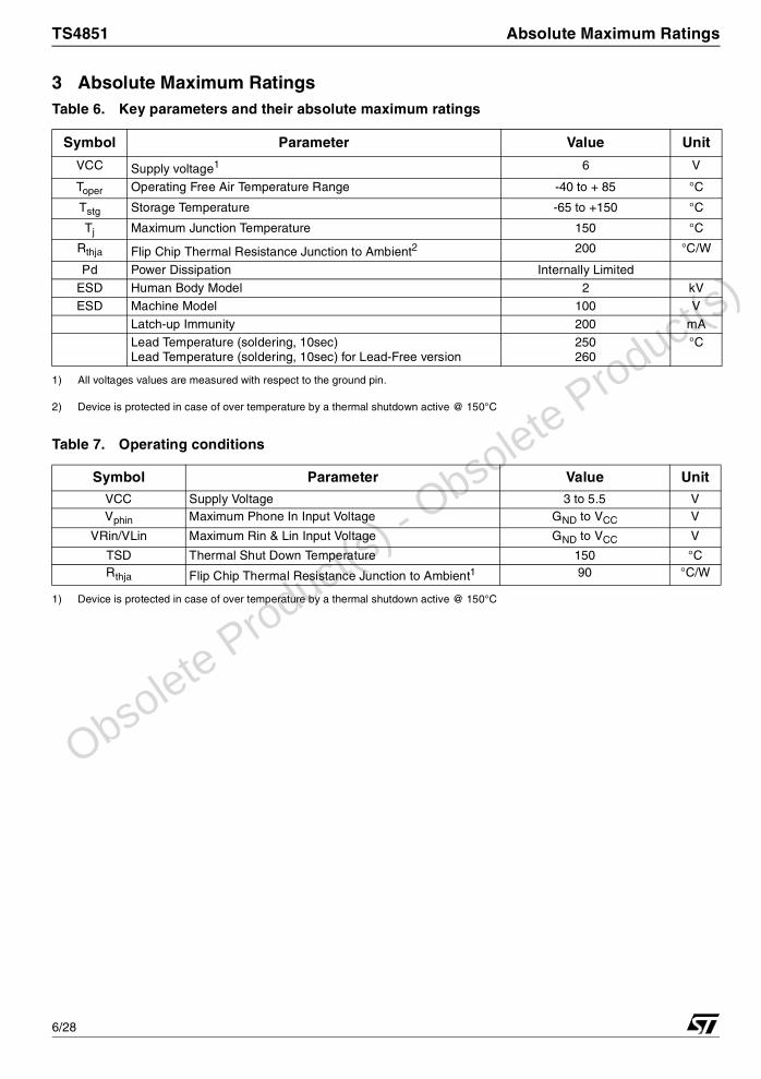
3 Absolute Maximum Ratings Table 6. Key parameters and their absolute maximum ratings
Symbol Parameter Value Unit
VCC Supply voltage1
1) All voltages values are measured with respect to the ground pin.
6 V
Toper Operating Free Air Temperature Range -40 to + 85 °C
Tstg Storage Temperature -65 to +150 °C
Tj Maximum Junction Temperature 150 °C
Rthja Flip Chip Thermal Resistance Junction to Ambient2
2) Device is protected in case of over temperature by a thermal shutdown active @ 150°C
200 °C/W
Pd Power Dissipation Internally LimitedESD Human Body Model 2 kVESD Machine Model 100 V
Latch-up Immunity 200 mALead Temperature (soldering, 10sec)Lead Temperature (soldering, 10sec) for Lead-Free version
250260
°C
Table 7. Operating conditions
Symbol Parameter Value Unit
VCC Supply Voltage 3 to 5.5 VVphin Maximum Phone In Input Voltage GND to VCC V
VRin/VLin Maximum Rin & Lin Input Voltage GND to VCC V
TSD Thermal Shut Down Temperature 150 °CRthja Flip Chip Thermal Resistance Junction to Ambient1
1) Device is protected in case of over temperature by a thermal shutdown active @ 150°C
90 °C/W
Obso
lete Product(s)
- Obso
lete Product(s)
6/28
Electrical Characteristics TS4851
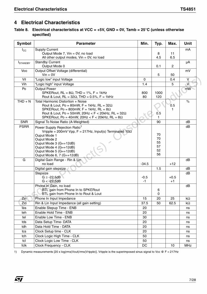
4 Electrical Characteristics Table 8. Electrical characteristics at VCC = +5V, GND = 0V, Tamb = 25°C (unless otherwise
specified)
Symbol Parameter Min. Typ. Max. Unit
ICC Supply Current Output Mode 7, Vin = 0V, no loadAll other output modes, Vin = 0V, no load
84.5
116.5
mA
ISTANDBY Standby CurrentOutput Mode 0 0.1 2
µA
Voo Output Offset Voltage (differential)Vin = 0V 5 50
mV
Vil “Logic low” input Voltage 0 0.4 VVih “Logic high” input Voltage 1.4 5 VPo Output Power
SPKERout, RL = 8Ω, THD = 1%, F = 1kHzRout & Lout, RL = 32Ω, THD = 0.5%, F = 1kHz
80080
1000120
mW
THD + N Total Harmonic Distortion + NoiseRout & Lout, Po = 80mW, F = 1kHz, RL = 32ΩSPKERout, Po = 800mW, F = 1kHz, RL = 8ΩRout & Lout, Po = 50mW, 20Hz < F < 20kHz, RL = 32ΩSPKERout, Po = 40mW, 20Hz < F < 20kHz, RL = 8Ω
0.51
0.51
%
SNR Signal To Noise Ratio (A-Weighted) 90 dBPSRR Power Supply Rejection Ratio1
Vripple = 200mV Vpp, F = 217Hz, Input(s) Terminated 10ΩOuput Mode 1Ouput Mode 2Ouput Mode 3 (G=+12dB)Ouput Mode 4 (G=+12dB)Ouput Mode 5 (G=+12dB)Ouput Mode 6, 7 (G=+12dB)
1) Dynamic measurements [20 x log(rms(Vout)/rms(Vripple)]. Vripple is the superimposed sinus signal to Vcc @ F = 217Hz
707055575256
dB
G Digital Gain Range - Rin & Linno load -34.5 +12
dB
Digital gain stepsize 1.5 dBStepsize
G ≥ -22.5dBG < -22.5dB
-0.5-1
+0.5+1
dB
Phone In Gain, no loadBTL gain from Phone In to SPKERoutBTL gain from Phone In to Rout & Lout
60
dB
Zin Phone In Input Impedance 15 20 25 kΩZin Rin & Lin Input Impedance (all gain setting) 37.5 50 62.5 kΩtes Enable Stepup Time - ENB 20 nsteh Enable Hold Time - ENB 20 nstel Enable Low Time - ENB 30 nstds Data Setup Time- DATA 20 nstdh Data Hold Time - DATA 20 nstcs Clock Setup time - CLK 20 nstch Clock Logic High Time - CLK 50 nstcl Clock Logic Low Time - CLK 50 nsfclk Clock Frequency - CLK DC 10 MHz
Obso
lete Product(s)
- Obso
lete Product(s)
7/28
TS4851 Electrical Characteristics
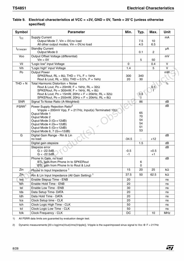
Table 9. Electrical characteristics at VCC = +3V, GND = 0V, Tamb = 25°C (unless otherwise specified)
Symbol Parameter Min. Typ. Max. Unit
ICC Supply Current Output Mode 7, Vin = 0V,no loadAll other output modes, Vin = 0V,no load
7.54.5
106.5
mA
ISTANDBY Standby CurrentOutput Mode 0 0.1 2
µA
Voo Output Offset Voltage (differential)Vin = 0V 5 50
mV
Vil “Logic low” input Voltage 0 0.4 VVih “Logic high” input Voltage 1.4 5 VPo Output Power
SPKERout, RL = 8Ω, THD = 1%, F = 1kHzRout & Lout, RL = 32Ω, THD = 0.5%, F = 1kHz
30020
34030
mW
THD + N Total Harmonic Distortion + NoiseRout & Lout, Po = 20mW, F = 1kHz, RL = 32ΩSPKERout, Po = 300mW, F = 1kHz, RL = 8ΩRout & Lout, Po = 15mW, 20Hz < F < 20kHz, RL = 32ΩSPKERout, Po = 250mW, 20Hz < F < 20kHz, RL = 8Ω
0.51
0.51
%
SNR Signal To Noise Ratio (A-Weighted) 86 dB
PSRR1 Power Supply Rejection Ratio2
Vripple = 200mV Vpp, F = 217Hz, Input(s) Terminated 10ΩOuput Mode 1Ouput Mode 2Ouput Mode 3 (G=+12dB)Ouput Mode 4 (G=+12dB)Ouput Mode 5 (G=+12dB)Ouput Mode 6, 7 (G=+12dB)
657054545153
dB
G Digital Gain Range - Rin & Linno load -34.5 - +12
dB
Digital gain stepsize 1.5 dBStepsize error
G ≥ -22.5dBG < -22.5dB
-0.5-1
+0.5+1
dB
Phone In Gain, no load BTL gain from Phone In to SPKERoutBTL gain from Phone In to Rout & Lout
60
dB
Zin Phone In Input Impedance 1 15 20 25 kΩ
Zin Rin & Lin Input Impedance (All Gain Setting) 1 37.5 50 62.5 kΩ
tes Enable Stepup Time - ENB 20 nsteh Enable Hold Time - ENB 20 nstel Enable Low Time - ENB 30 nstds Data Setup Time- DATA 20 nstdh Data Hold Time - DATA 20 nstcs Clock Setup time - CLK 20 nstch Clock Logic High Time - CLK 50 nstcl Clock Logic Low Time - CLK 50 nsfclk Clock Frequency - CLK DC 10 MHz
1) All PSRR data limits are guaranted by evaluation desgin test.
2) Dynamic measurements [20 x log(rms(Vout)/rms(Vripple)]. Vripple is the superimposed sinus signal to Vcc @ F = 217Hz
Obso
lete Product(s)
- Obso
lete Product(s)
8/28
Electrical Characteristics TS4851
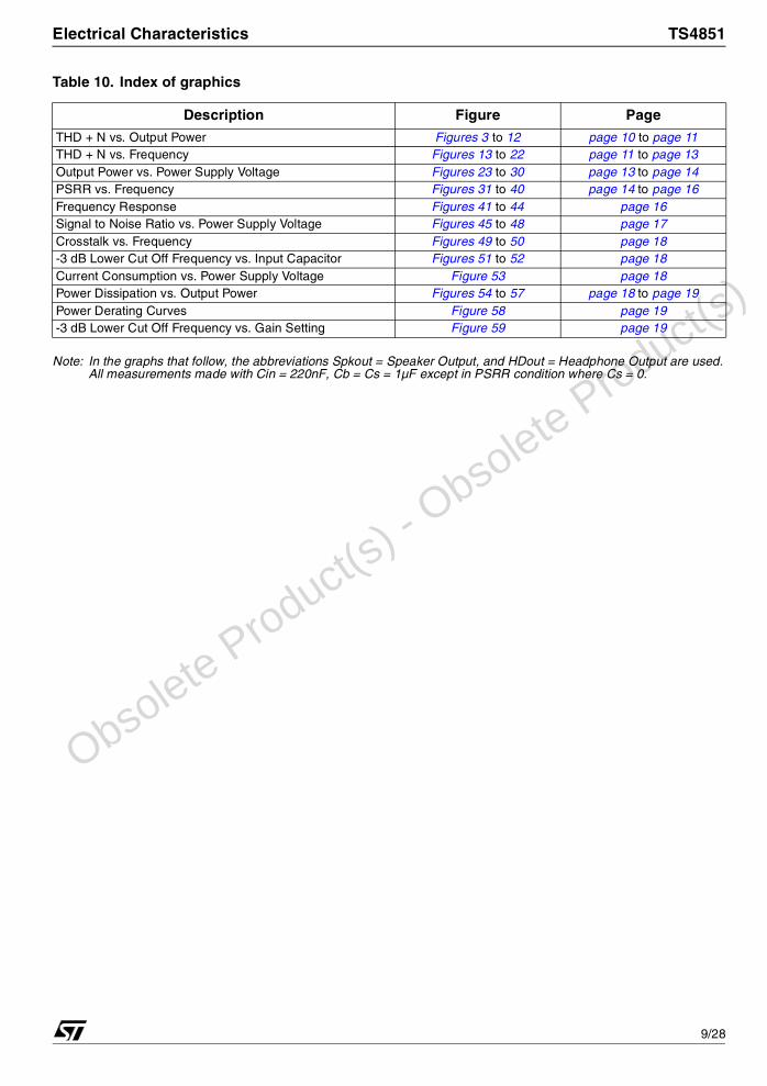
Note: In the graphs that follow, the abbreviations Spkout = Speaker Output, and HDout = Headphone Output are used.All measurements made with Cin = 220nF, Cb = Cs = 1µF except in PSRR condition where Cs = 0.
Table 10. Index of graphics
Description Figure Page
THD + N vs. Output Power Figures 3 to 12 page 10 to page 11THD + N vs. Frequency Figures 13 to 22 page 11 to page 13Output Power vs. Power Supply Voltage Figures 23 to 30 page 13 to page 14PSRR vs. Frequency Figures 31 to 40 page 14 to page 16Frequency Response Figures 41 to 44 page 16 Signal to Noise Ratio vs. Power Supply Voltage Figures 45 to 48 page 17Crosstalk vs. Frequency Figures 49 to 50 page 18 -3 dB Lower Cut Off Frequency vs. Input Capacitor Figures 51 to 52 page 18 Current Consumption vs. Power Supply Voltage Figure 53 page 18Power Dissipation vs. Output Power Figures 54 to 57 page 18 to page 19Power Derating Curves Figure 58 page 19-3 dB Lower Cut Off Frequency vs. Gain Setting Figure 59 page 19
Obso
lete Product(s)
- Obso
lete Product(s)
9/28
TS4851 Electrical Characteristics
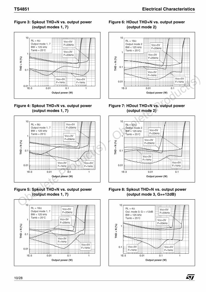
Figure 3: Spkout THD+N vs. output power(output modes 1, 7)
Figure 4: Spkout THD+N vs. output power(output modes 1, 7)
Figure 5: Spkout THD+N vs. output power(output modes 1, 7)
Figure 6: HDout THD+N vs. output power (output mode 2)
Figure 7: HDout THD+N vs. output power(output mode 2)
Figure 8: Spkout THD+N vs. output power(output mode 3, G=+12dB)
1E-3 0.01 0.1 10.01
0.1
1
10
Vcc=5VF=20kHz
Vcc=5VF=1kHz
Vcc=3VF=20kHz
Vcc=3VF=1kHz
RL = 4ΩOutput mode 1, 7BW < 125 kHzTamb = 25°C
TH
D +
N (
%)
Output power (W)
1E-3 0.01 0.1 1
0.01
0.1
1
10Vcc=5VF=20kHz
Vcc=5VF=1kHz
Vcc=3VF=20kHz
Vcc=3VF=1kHz
RL = 8ΩOutput mode 1, 7BW < 125 kHzTamb = 25°C
TH
D +
N (
%)
Output power (W)
1E-3 0.01 0.1 1
0.01
0.1
1
10
Vcc=5VF=20kHz
Vcc=5VF=1kHz
Vcc=3VF=20kHz
Vcc=3VF=1kHz
RL = 16ΩOutput mode 1, 7BW < 125 kHzTamb = 25°C
TH
D +
N (
%)
Output power (W)
1E-3 0.01 0.1
0.01
0.1
1
10
Vcc=5VF=20kHz
Vcc=5VF=1kHz
Vcc=3VF=20kHz
Vcc=3VF=1kHz
RL = 16ΩOutput mode 2BW < 125 kHzTamb = 25°C
TH
D +
N (
%)
Output power (W)
1E-3 0.01 0.1
0.01
0.1
1
10
Vcc=5VF=20kHz
Vcc=5VF=1kHz
Vcc=3VF=20kHz
Vcc=3VF=1kHz
RL = 32ΩOutput mode 2BW < 125 kHzTamb = 25°C
TH
D +
N (
%)
Output power (W)
1E-3 0.01 0.1 1
0.1
1
10
Vcc=5VF=20kHz
Vcc=5VF=1kHz
Vcc=3VF=20kHz
Vcc=3VF=1kHz
RL = 4ΩOut. mode 3; G = +12dBBW < 125 kHzTamb = 25°C
TH
D +
N (
%)
Output power (W)
Obso
lete Product(s)
- Obso
lete Product(s)
10/28
Electrical Characteristics TS4851
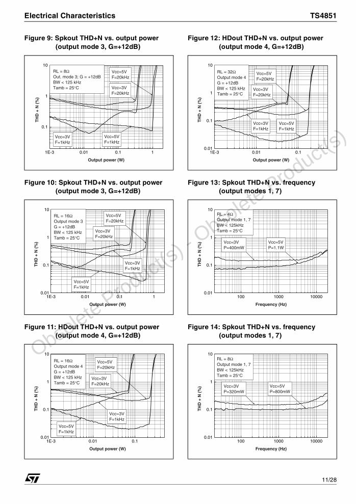
Figure 9: Spkout THD+N vs. output power(output mode 3, G=+12dB)
Figure 10: Spkout THD+N vs. output power(output mode 3, G=+12dB)
Figure 11: HDout THD+N vs. output power(output mode 4, G=+12dB)
Figure 12: HDout THD+N vs. output power (output mode 4, G=+12dB)
Figure 13: Spkout THD+N vs. frequency(output modes 1, 7)
Figure 14: Spkout THD+N vs. frequency(output modes 1, 7)
1E-3 0.01 0.1 1
0.1
1
10
Vcc=5VF=20kHz
Vcc=5VF=1kHz
Vcc=3VF=20kHz
Vcc=3VF=1kHz
RL = 8ΩOut. mode 3; G = +12dBBW < 125 kHzTamb = 25°C
TH
D +
N (
%)
Output power (W)
1E-3 0.01 0.1 10.01
0.1
1
10Vcc=5VF=20kHz
Vcc=5VF=1kHz
Vcc=3VF=20kHz
Vcc=3VF=1kHz
RL = 16ΩOutput mode 3G = +12dBBW < 125 kHzTamb = 25°C
TH
D +
N (
%)
Output power (W)
1E-3 0.01 0.10.01
0.1
1
10
Vcc=5VF=20kHz
Vcc=5VF=1kHz
Vcc=3VF=20kHz
Vcc=3VF=1kHz
RL = 16ΩOutput mode 4G = +12dBBW < 125 kHzTamb = 25°C
TH
D +
N (
%)
Output power (W)
1E-3 0.01 0.10.01
0.1
1
10
Vcc=5VF=20kHz
Vcc=5VF=1kHz
Vcc=3VF=20kHz
Vcc=3VF=1kHz
RL = 32ΩOutput mode 4G = +12dBBW < 125 kHzTamb = 25°C
TH
D +
N (
%)
Output power (W)
100 1000 100000.01
0.1
1
10
Vcc=5VP=1.1W
Vcc=3VP=400mW
RL = 4ΩOutput mode 1, 7BW < 125kHzTamb = 25°C
TH
D +
N (
%)
Frequency (Hz)
100 1000 100000.01
0.1
1
10
Vcc=5VP=800mW
Vcc=3VP=320mW
RL = 8ΩOutput mode 1, 7BW < 125kHzTamb = 25°C
TH
D +
N (
%)
Frequency (Hz)
Obso
lete Product(s)
- Obso
lete Product(s)
11/28
TS4851 Electrical Characteristics
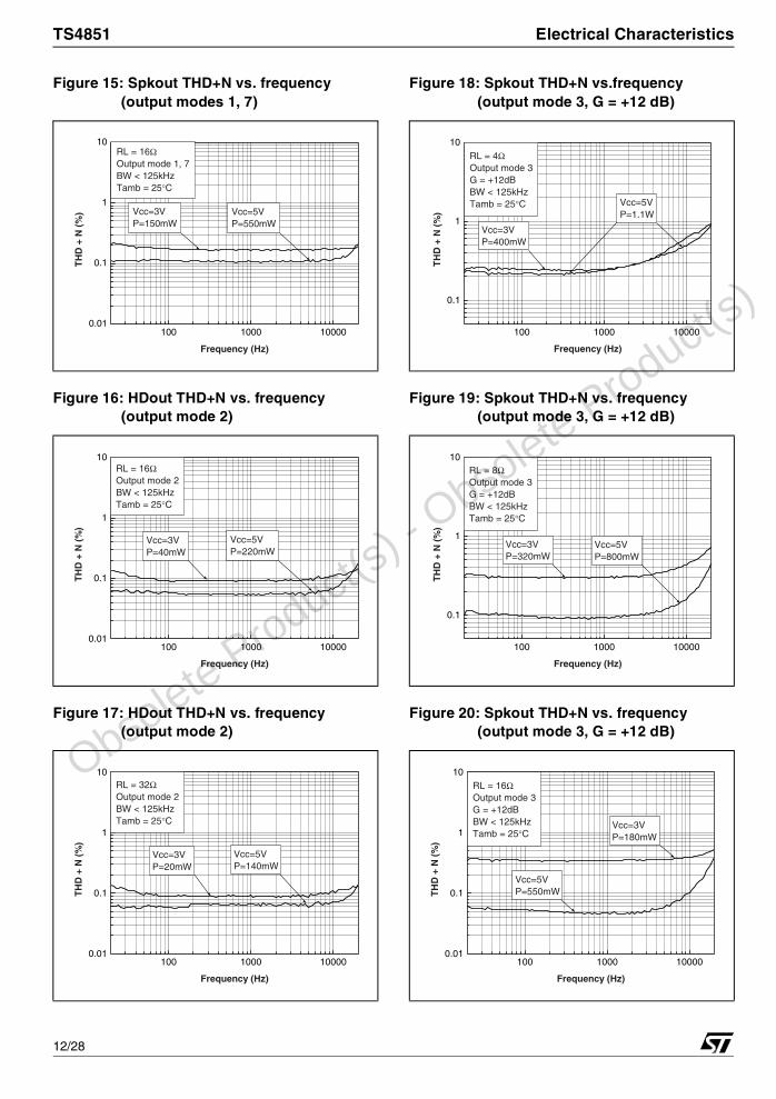
Figure 15: Spkout THD+N vs. frequency(output modes 1, 7)
Figure 16: HDout THD+N vs. frequency(output mode 2)
Figure 17: HDout THD+N vs. frequency(output mode 2)
Figure 18: Spkout THD+N vs.frequency(output mode 3, G = +12 dB)
Figure 19: Spkout THD+N vs. frequency(output mode 3, G = +12 dB)
Figure 20: Spkout THD+N vs. frequency(output mode 3, G = +12 dB)
100 1000 100000.01
0.1
1
10
Vcc=5VP=550mW
Vcc=3VP=150mW
RL = 16ΩOutput mode 1, 7BW < 125kHzTamb = 25°C
TH
D +
N (
%)
Frequency (Hz)
100 1000 100000.01
0.1
1
10
Vcc=5VP=220mW
Vcc=3VP=40mW
RL = 16ΩOutput mode 2BW < 125kHzTamb = 25°C
TH
D +
N (
%)
Frequency (Hz)
100 1000 100000.01
0.1
1
10
Vcc=5VP=140mW
Vcc=3VP=20mW
RL = 32ΩOutput mode 2BW < 125kHzTamb = 25°C
TH
D +
N (
%)
Frequency (Hz)
100 1000 10000
0.1
1
10
Vcc=5VP=1.1W
Vcc=3VP=400mW
RL = 4ΩOutput mode 3G = +12dBBW < 125kHzTamb = 25°C
TH
D +
N (
%)
Frequency (Hz)
100 1000 10000
0.1
1
10
Vcc=5VP=800mW
Vcc=3VP=320mW
RL = 8ΩOutput mode 3G = +12dBBW < 125kHzTamb = 25°C
TH
D +
N (
%)
Frequency (Hz)
100 1000 100000.01
0.1
1
10
Vcc=5VP=550mW
Vcc=3VP=180mW
RL = 16ΩOutput mode 3G = +12dBBW < 125kHzTamb = 25°C
TH
D +
N (
%)
Frequency (Hz)
Obso
lete Product(s)
- Obso
lete Product(s)
12/28
Electrical Characteristics TS4851
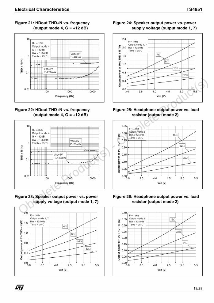
Figure 21: HDout THD+N vs. frequency(output mode 4, G = +12 dB)
Figure 22: HDout THD+N vs. frequency(output mode 4, G = +12 dB)
Figure 23: Speaker output power vs. power supply voltage (output mode 1, 7)
Figure 24: Speaker output power vs. power supply voltage (output mode 1, 7)
Figure 25: Headphone output power vs. load resistor (output mode 2)
Figure 26: Headphone output power vs. load resistor (output mode 2)
100 1000 100000.01
0.1
1
10
Vcc=5VP=220mW
Vcc=3VP=40mW
RL = 16ΩOutput mode 4G = +12dBBW < 125kHzTamb = 25°C
TH
D +
N (
%)
Frequency (Hz)
100 1000 100000.01
0.1
1
10
Vcc=5VP=140mW
Vcc=3VP=20mW
RL = 32ΩOutput mode 4G = +12dBBW < 125kHzTamb = 25°C
TH
D +
N (
%)
Frequency (Hz)
3.0 3.5 4.0 4.5 5.0 5.50.0
0.4
0.8
1.2
1.6
2.0F = 1kHzOutput mode 1, 7BW < 125kHzTamb = 25°C
32Ω
16Ω
8Ω
4Ω
Ou
tpu
t p
ow
er a
t 1%
TH
D +
N (
W)
Vcc (V)
3.0 3.5 4.0 4.5 5.0 5.50.0
0.4
0.8
1.2
1.6
2.0
2.4F = 1kHzOutput mode 1, 7BW < 125kHzTamb = 25°C
32Ω
16Ω
8Ω
4Ω
Ou
tpu
t p
ow
er a
t 10
% T
HD
+ N
(W
)
Vcc (V)
3.0 3.5 4.0 4.5 5.0 5.50.00
0.05
0.10
0.15
0.20
0.25
0.30
0.35F = 1kHzOutput mode 2BW < 125kHzTamb = 25°C
32Ω
16Ω
64Ω
Ou
tpu
t p
ow
er a
t 1%
TH
D +
N (
W)
Vcc (V)
3.0 3.5 4.0 4.5 5.0 5.50.00
0.05
0.10
0.15
0.20
0.25
0.30
0.35
0.40F = 1kHzOutput mode 2BW < 125kHzTamb = 25°C
32Ω
16Ω
64Ω
Ou
tpu
t p
ow
er a
t 10
% T
HD
+ N
(W
)
Vcc (V)
Obso
lete Product(s)
- Obso
lete Product(s)
13/28
TS4851 Electrical Characteristics
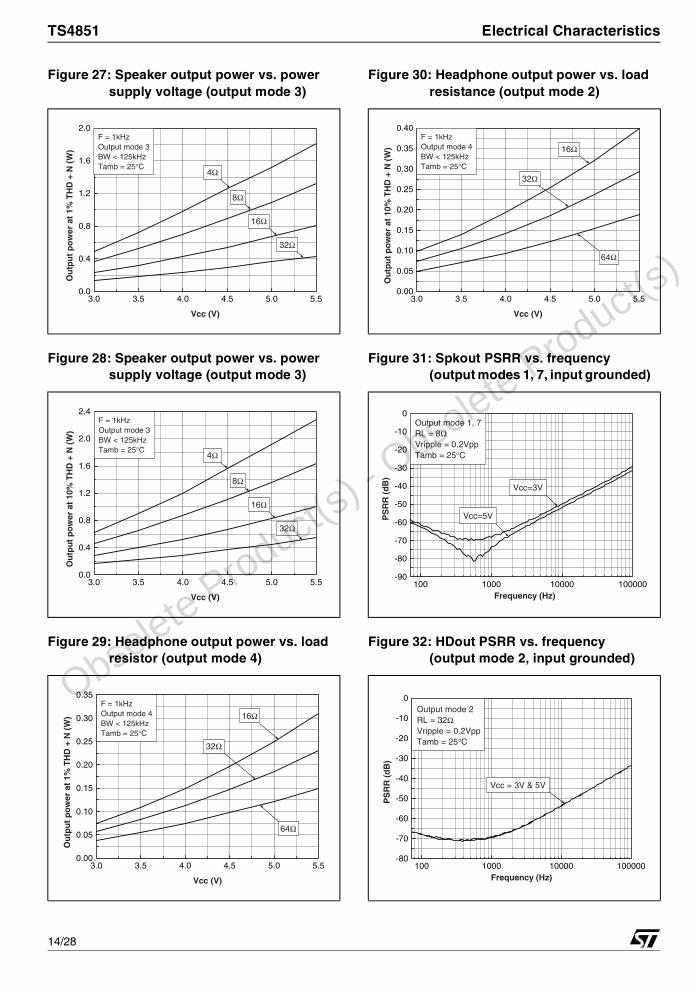
Figure 27: Speaker output power vs. power supply voltage (output mode 3)
Figure 28: Speaker output power vs. power supply voltage (output mode 3)
Figure 29: Headphone output power vs. load resistor (output mode 4)
Figure 30: Headphone output power vs. load resistance (output mode 2)
Figure 31: Spkout PSRR vs. frequency(output modes 1, 7, input grounded)
Figure 32: HDout PSRR vs. frequency(output mode 2, input grounded)
3.0 3.5 4.0 4.5 5.0 5.50.0
0.4
0.8
1.2
1.6
2.0F = 1kHzOutput mode 3BW < 125kHzTamb = 25°C
32Ω
16Ω
8Ω
4Ω
Ou
tpu
t p
ow
er a
t 1%
TH
D +
N (
W)
Vcc (V)
3.0 3.5 4.0 4.5 5.0 5.50.0
0.4
0.8
1.2
1.6
2.0
2.4F = 1kHzOutput mode 3BW < 125kHzTamb = 25°C
32Ω
16Ω
8Ω
4Ω
Ou
tpu
t p
ow
er a
t 10
% T
HD
+ N
(W
)
Vcc (V)
3.0 3.5 4.0 4.5 5.0 5.50.00
0.05
0.10
0.15
0.20
0.25
0.30
0.35F = 1kHzOutput mode 4BW < 125kHzTamb = 25°C
32Ω
16Ω
64Ω
Ou
tpu
t p
ow
er a
t 1%
TH
D +
N (
W)
Vcc (V)
3.0 3.5 4.0 4.5 5.0 5.50.00
0.05
0.10
0.15
0.20
0.25
0.30
0.35
0.40F = 1kHzOutput mode 4BW < 125kHzTamb = 25°C
32Ω
16Ω
64Ω
Ou
tpu
t p
ow
er a
t 10
% T
HD
+ N
(W
)
Vcc (V)
100 1000 10000 100000-90
-80
-70
-60
-50
-40
-30
-20
-10
0
Vcc=3V
Vcc=5V
Output mode 1, 7RL = 8ΩVripple = 0.2VppTamb = 25°C
PS
RR
(d
B)
Frequency (Hz)
100 1000 10000 100000-80
-70
-60
-50
-40
-30
-20
-10
0
Vcc = 3V & 5V
Output mode 2RL = 32ΩVripple = 0.2VppTamb = 25°C
PS
RR
(d
B)
Frequency (Hz)
Obso
lete Product(s)
- Obso
lete Product(s)
14/28
Electrical Characteristics TS4851
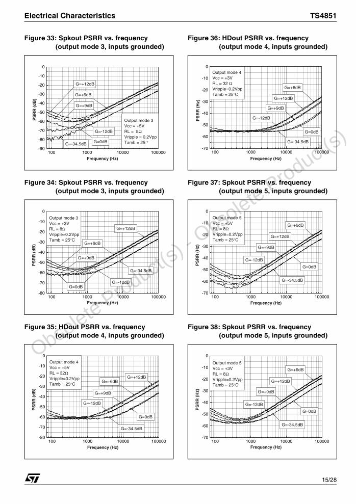
Figure 33: Spkout PSRR vs. frequency(output mode 3, inputs grounded)
Figure 34: Spkout PSRR vs. frequency(output mode 3, inputs grounded)
Figure 35: HDout PSRR vs. frequency(output mode 4, inputs grounded)
Figure 36: HDout PSRR vs. frequency(output mode 4, inputs grounded)
Figure 37: Spkout PSRR vs. frequency(output mode 5, inputs grounded)
Figure 38: Spkout PSRR vs. frequency(output mode 5, inputs grounded)
100 1000 10000 100000-90
-80
-70
-60
-50
-40
-30
-20
-10
0
G=-34.5dB
G=-12dB
G=0dB
G=+9dB
G=+6dB
G=+12dB
Output mode 3Vcc = +5VRL = 8ΩVripple = 0.2VppTamb = 25 °
PS
RR
(d
B)
Frequency (Hz)
100 1000 10000 100000-80
-70
-60
-50
-40
-30
-20
-10
0
G=-34.5dB
G=-12dBG=0dB
G=+6dB
G=+9dB
G=+12dB
Output mode 3Vcc = +3VRL = 8ΩVripple=0.2VppTamb = 25°C
PS
RR
(d
B)
Frequency (Hz)
100 1000 10000 100000-80
-70
-60
-50
-40
-30
-20
-10
0
G=-34.5dB
G=-12dB
G=0dB
G=+6dB
G=+9dB
G=+12dB
Output mode 4Vcc = +5VRL = 32ΩVripple=0.2VppTamb = 25°C
PS
RR
(d
B)
Frequency (Hz)
100 1000 10000 100000-70
-60
-50
-40
-30
-20
-10
0
G=-34.5dB
G=-12dB
G=0dB
G=+6dB
G=+9dB
G=+12dB
Output mode 4Vcc = +3VRL = 32 ΩVripple=0.2VppTamb = 25°C
PS
RR
(H
z)
Frequency (Hz)
100 1000 10000 100000-70
-60
-50
-40
-30
-20
-10
0
G=-34.5dB
G=-12dB
G=0dB
G=+6dB
G=+9dB
G=+12dB
Output mode 5Vcc = +5VRL = 8ΩVripple=0.2VppTamb = 25°C
PS
RR
(H
z)
Frequency (Hz)
100 1000 10000 100000-70
-60
-50
-40
-30
-20
-10
0
G=-34.5dB
G=-12dB
G=0dB
G=+6dB
G=+9dB
G=+12dB
Output mode 5Vcc = +3VRL = 8ΩVripple=0.2VppTamb = 25°C
PS
RR
(H
z)
Frequency (Hz)
Obso
lete Product(s)
- Obso
lete Product(s)
15/28
TS4851 Electrical Characteristics
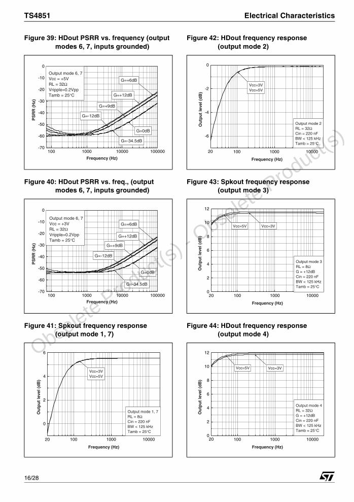
Figure 39: HDout PSRR vs. frequency (output modes 6, 7, inputs grounded)
Figure 40: HDout PSRR vs. freq., (output modes 6, 7, inputs grounded)
Figure 41: Spkout frequency response(output mode 1, 7)
Figure 42: HDout frequency response(output mode 2)
Figure 43: Spkout frequency response(output mode 3)
Figure 44: HDout frequency response(output mode 4)
100 1000 10000 100000-70
-60
-50
-40
-30
-20
-10
0
G=-34.5dB
G=-12dB
G=0dB
G=+6dB
G=+9dB
G=+12dB
Output mode 6, 7Vcc = +5VRL = 32ΩVripple=0.2VppTamb = 25°C
PS
RR
(H
z)
Frequency (Hz)
100 1000 10000 100000-70
-60
-50
-40
-30
-20
-10
0
G=-34.5dB
G=-12dB
G=0dB
G=+6dB
G=+9dB
G=+12dB
Output mode 6, 7Vcc = +3VRL = 32ΩVripple=0.2VppTamb = 25°C
PS
RR
(H
z)
Frequency (Hz)
100 1000 10000
0
2
4
6
20
Output mode 1, 7RL = 8ΩCin = 220 nFBW < 125 kHzTamb = 25°C
Vcc=3VVcc=5V
Ou
tpu
t le
vel (
dB
)
Frequency (Hz)
100 1000 10000
-6
-4
-2
0
20
Output mode 2RL = 32ΩCin = 220 nFBW < 125 kHzTamb = 25°C
Vcc=3VVcc=5V
Ou
tpu
t le
vel (
dB
)
Frequency (Hz)
100 1000 100000
2
4
6
8
10
12
20
Vcc=5V
Output mode 3RL = 8ΩG = +12dBCin = 220 nFBW < 125 kHzTamb = 25°C
Vcc=3V
Ou
tpu
t le
vel (
dB
)
Frequency (Hz)
100 1000 100000
2
4
6
8
10
12
20
Vcc=5V
Output mode 4RL = 32ΩG = +12dBCin = 220 nFBW < 125 kHzTamb = 25°C
Vcc=3V
Ou
tpu
t le
vel (
dB
)
Frequency (Hz)
Obso
lete Product(s)
- Obso
lete Product(s)
16/28
Electrical Characteristics TS4851
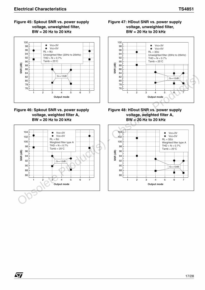
Figure 45: Spkout SNR vs. power supply voltage, unweighted filter, BW = 20 Hz to 20 kHz
Figure 46: Spkout SNR vs. power supply voltage, weighted filter A, BW = 20 Hz to 20 kHz
Figure 47: HDout SNR vs. power supply voltage, unweighted filter, BW = 20 Hz to 20 kHz
Figure 48: HDout SNR vs. power supply voltage, weighted filter A, BW = 20 Hz to 20 kHz
1 2 3 4 5 6 7
76
78
80
82
84
86
88
90
92
94
96
98
100
G=+12dB
Vcc=3V Vcc=5V
RL = 8ΩUnweighted filter (20Hz to 20kHz)THD + N < 0.7%Tamb = 25°C
SN
R (
dB
)
Output mode
1 2 3 4 5 6 7
86
88
90
92
94
96
98
100
102
104
G=+12dB
Vcc=3V Vcc=5V
RL = 8ΩWeighted filter type ATHD + N < 0.7%Tamb = 25°C
SN
R (
dB
)
Output mode
1 2 3 4 5 6 7
76
78
80
82
84
86
88
90
92
94
96
98
100
G=+12dB
Vcc=3V Vcc=5V
RL = 32ΩUnweighted filter (20Hz to 20kHz)THD + N < 0.7%Tamb = 25°C
SN
R (
dB
)
Output mode
1 2 3 4 5 6 7
86
88
90
92
94
96
98
100
102
104
G=+12dB
Vcc=3V Vcc=5V
RL = 32ΩWeighted filter type ATHD + N < 0.7%Tamb = 25°C
SN
R (
dB
)
Output mode
Obso
lete Product(s)
- Obso
lete Product(s)
17/28
TS4851 Electrical Characteristics
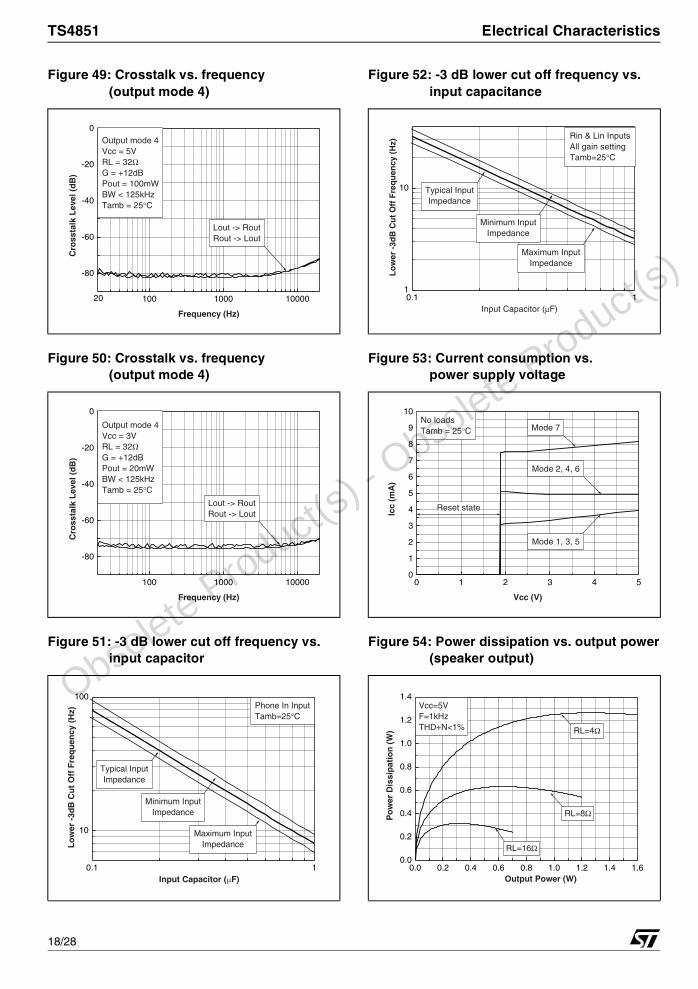
Figure 49: Crosstalk vs. frequency(output mode 4)
Figure 50: Crosstalk vs. frequency(output mode 4)
Figure 51: -3 dB lower cut off frequency vs. input capacitor
Figure 52: -3 dB lower cut off frequency vs. input capacitance
Figure 53: Current consumption vs.power supply voltage
Figure 54: Power dissipation vs. output power(speaker output)
100 1000 10000
-80
-60
-40
-20
0
20
Lout -> RoutRout -> Lout
Output mode 4Vcc = 5VRL = 32ΩG = +12dBPout = 100mWBW < 125kHzTamb = 25°C
Cro
ssta
lk L
evel
(d
B)
Frequency (Hz)
100 1000 10000
-80
-60
-40
-20
0
Lout -> RoutRout -> Lout
Output mode 4Vcc = 3VRL = 32ΩG = +12dBPout = 20mWBW < 125kHzTamb = 25°C
Cro
ssta
lk L
evel
(d
B)
Frequency (Hz)
0.1 1
10
100
Minimum InputImpedance
Maximum InputImpedance
Typical InputImpedance
Phone In InputTamb=25°C
Lo
wer
-3d
B C
ut
Off
Fre
qu
ency
(H
z)
Input Capacitor ( F)
0.1 11
10
Minimum InputImpedance
Maximum InputImpedance
Typical InputImpedance
Rin & Lin InputsAll gain settingTamb=25°C
Lo
wer
-3d
B C
ut
Off
Fre
qu
ency
(H
z)
Input Capacitor (µF)
0 1 2 3 4 50
1
2
3
4
5
6
7
8
9
10No loadsTamb = 25°C
Reset state
Mode 1, 3, 5
Mode 2, 4, 6
Mode 7
Icc
(mA
)
Vcc (V)
0.0 0.2 0.4 0.6 0.8 1.0 1.2 1.4 1.60.0
0.2
0.4
0.6
0.8
1.0
1.2
1.4
RL=16Ω
RL=8Ω
Vcc=5VF=1kHzTHD+N<1% RL=4Ω
Po
wer
Dis
sip
atio
n (
W)
Output Power (W)
Obso
lete Product(s)
- Obso
lete Product(s)
18/28
Electrical Characteristics TS4851
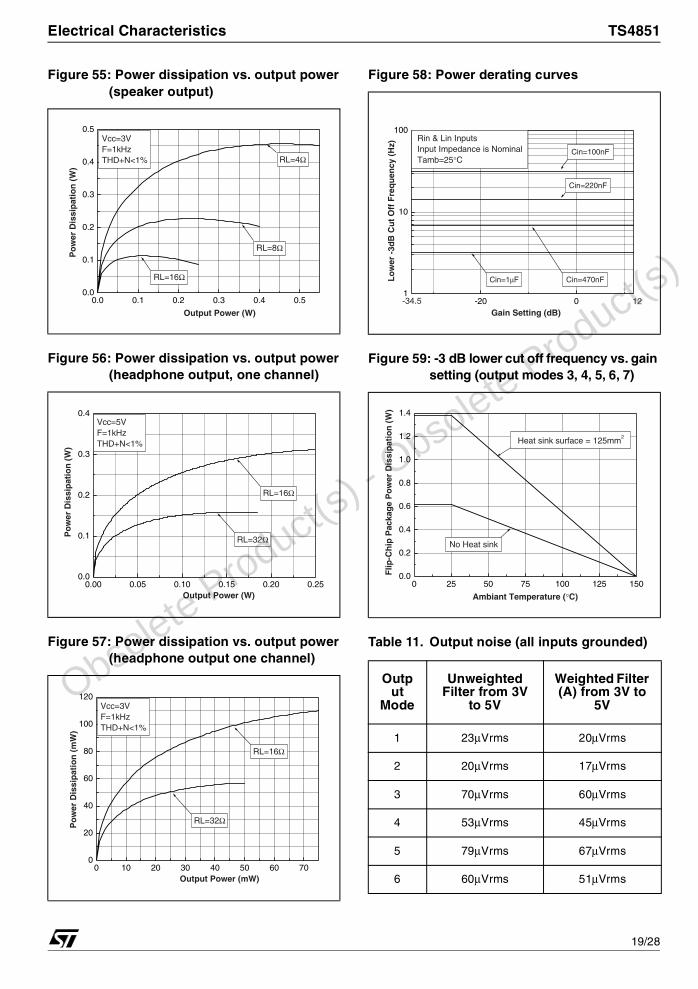
Figure 55: Power dissipation vs. output power(speaker output)
Figure 56: Power dissipation vs. output power(headphone output, one channel)
Figure 57: Power dissipation vs. output power(headphone output one channel)
Figure 58: Power derating curves
Figure 59: -3 dB lower cut off frequency vs. gain setting (output modes 3, 4, 5, 6, 7)
Table 11. Output noise (all inputs grounded)
0.0 0.1 0.2 0.3 0.4 0.50.0
0.1
0.2
0.3
0.4
0.5
RL=4Ω
RL=8Ω
Vcc=3VF=1kHzTHD+N<1%
RL=16Ω
Po
wer
Dis
sip
atio
n (
W)
Output Power (W)
0.00 0.05 0.10 0.15 0.20 0.250.0
0.1
0.2
0.3
0.4
RL=16Ω
RL=32Ω
Vcc=5VF=1kHzTHD+N<1%
Po
wer
Dis
sip
atio
n (
W)
Output Power (W)
0 10 20 30 40 50 60 700
20
40
60
80
100
120
RL=32Ω
Vcc=3VF=1kHzTHD+N<1%
RL=16Ω
Po
wer
Dis
sip
atio
n (
mW
)
Output Power (mW)
Output
Mode
Unweighted Filter from 3V
to 5V
Weighted Filter (A) from 3V to
5V
1 23µVrms 20µVrms
2 20µVrms 17µVrms
3 70µVrms 60µVrms
4 53µVrms 45µVrms
5 79µVrms 67µVrms
6 60µVrms 51µVrms
-20 01
10
100
Cin=1µF Cin=470nF
Cin=220nF
Cin=100nF
Rin & Lin InputsInput Impedance is NominalTamb=25°C
12-34.5
Lo
wer
-3d
B C
ut
Off
Fre
qu
ency
(H
z)
Gain Setting (dB)
0 25 50 75 100 125 1500.0
0.2
0.4
0.6
0.8
1.0
1.2
1.4
No Heat sink
Heat sink surface = 125mm2
Flip
-Ch
ip P
acka
ge
Po
wer
Dis
sip
atio
n (
W)
Ambiant Temperature ( C)
Obso
lete Product(s)
- Obso
lete Product(s)
19/28
TS4851 Application Information
5 Application Information
5.1 BTL configuration principles
The TS4851 integrates 3 monolithic power amplifier having BTL output. BTL (Bridge Tied Load) meansthat each end of the load is connected to two single-ended output amplifiers. Thus, we have:
Single ended output 1 = Vout1 = Vout (V)Single ended output 2 = Vout2 = -Vout (V)
and
Vout1 - Vout2 = 2Vout (V)
The output power is:
For the same power supply voltage, the output power in BTL configuration is four times higher than theoutput power in single ended configuration.
5.2 Power dissipation and efficiency
Hypotheses:
Voltage and current in the load are sinusoidal (Vout and Iout).
Supply voltage is a pure DC source (Vcc).
Regarding the load we have:
and
and
Then, the average current delivered by the supply voltage is:
The power delivered by the supply voltage is:
Psupply = Vcc IccAVG (W)
Then, the power dissipated by each amplifier isPdiss = Psupply - Pout (W)
)W(R
)Vout2(Pout
L
2RMS=
VOUT = VPEAK sinω t (V)
IOUT = VOUT RL
----------------- (A)
POUT = VPEAK 2 2RL
---------------------- (W)
ICC AVG = 2VPEA K πRL
-------------------- (A)
)W(PPR
V22P OUTOUT
L
CCdiss −
π=
Obso
lete Product(s)
- Obso
lete Product(s)
20/28
Application Information TS4851
and the maximum value is obtained when:
and its value is:
Note: This maximum value is depends only on power supply voltage and load values.
The efficiency is the ratio between the output power and the power supply:
The maximum theoretical value is reached when Vpeak = Vcc, so:
The TS4851 has three independent power amplifiers. Each amplifier produces heat due to its powerdissipation. Therefore, the maximum die temperature is the sum of each amplifier’s maximum powerdissipation. It is calculated as follows:
Pdiss speaker = Power dissipation due to the speaker power amplifier.
Pdiss head = Power dissipation due to the Headphone power amplifier
Total Pdiss = Pdiss speaker + Pdiss head1 + Pdiss head2 (W)
In most cases, Pdiss head1 = Pdiss head2, giving:
Total Pdiss = Pdiss speaker + 2Pdiss head (W)
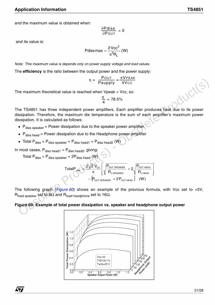
The following graph (Figure 60) shows an example of the previous formula, with Vcc set to +5V,Rload speaker set to 8Ω and Rload headphone set to 16Ω.
Figure 60: Example of total power dissipation vs. speaker and headphone output power
∂Pdiss ∂POUT
---------------------- = 0
)W(R
Vcc2maxPdiss
L2
2
π=
η = POUT
Psupply------------------------ = πVPEAK
4VCC-----------------------
π 4----- = 78.5%
[ ] )W(P2P
R
P2
R
PV22TotalP
HEADOUTSPEAKEROUT
HEADL
HEADOUT
SPEAKERL
SPEAKEROUTCCdiss
+−⎥⎥⎦
⎤
⎢⎢⎣
⎡+
π=
Obso
lete Product(s)
- Obso
lete Product(s)
21/28
TS4851 Application Information
5.3 Low frequency response
In low frequency region, the effect of Cin starts. Cin with Zin forms a high pass filter with a -3dB cut offfrequency.
Zin is the input impedance of the corresponding input:
• 20kΩ for Phone In IHF input
• 50kΩ for the 3 other inputs
Note: For all inputs, the impedance value remains constant for all gain settings. This means that the lower cut-offfrequency doesn’t change with gain setting. Note also that 20kΩ and 50kΩ are typical values and there aretolerances around these values (see Electrical Characteristics on page 7).
In Figures 39 to 41, you could easily establish the Cin value for a -3dB cut-off frequency required.
5.4 Decoupling of the circuit
Two capacitors are needed to bypass properly the TS4851, a power supply bypass capacitor Cs and abias voltage bypass capacitor Cb.
Cs has especially an influence on the THD+N in high frequency (above 7kHz) and indirectly on the powersupply disturbances.
With 1µF, you could expect similar THD+N performances like shown in the datasheet.
If Cs is lower than 1µF, THD+N increases in high frequency and disturbances on the power supply rail areless filtered.
To the contrary, if Cs is higher than 1µF, those disturbances on the power supply rail are more filtered.
Cb has an influence on THD+N in lower frequency, but its value is critical on the final result of PSRR withinput grounded in lower frequency:
• If Cb is lower than 1µF, THD+N increases at lower frequencies and the PSRR worsens upwards.
• If Cb is higher than 1µF, the benefit on THD+N and PSRR in the lower frequency range is small.
5.5 Startup time
When the TS4851 is controlled to switch from the full standby mode (output mode 0) to another outputmode, a delay is necessary to stabilize the DC bias. This delay depends on the Cb value and can becalculated by the following formulas.
Typical startup time = 0.0175 x Cb (s)
Max. startup time = 0.025 x Cb (s)(Cb is in µF in these formulas)
These formulas assume that the Cb voltage is equal to 0V. If the Cb voltage is not equal to 0V, the startuptime will be always lower.The startup time is the delay between the negative edge of Enable input (see Description of SPI operationon page 3) and the power ON of the output amplifiers.
Note: When the TS4851 is set in full standby mode, Cb is discharged through an internal switch.. The time to reach 0Vof Cb voltage is about ms.
)Hz(CinZin2
1FCL π
=
Obso
lete Product(s)
- Obso
lete Product(s)
22/28
Application Information TS4851
5.6 Pop and Click performance
The TS4851 has internal Pop and Click reduction circuitry. The performance of this circuitry is closelylinked with the value of the input capacitor Cin and the bias voltage bypass capacitor Cb.
The value of Cin is due to the lower cut-off frequency value requested. The value of Cb is due to THD+Nand PSRR requested always in lower frequency.
The TS4851 is optimized to have a low pop and click in the typical schematic configuration (see page 2).
Note: The value of Cs is not an important consideration as regards pop and click.
5.7 Notes on PSRR measurement
What is the PSRR?
The PSRR is the Power Supply Rejection Ratio. The PSRR of a device, is the ratio between a powersupply disturbance and the result on the output. We can say that the PSRR is the ability of a device tominimize the impact of power supply disturbances to the output.
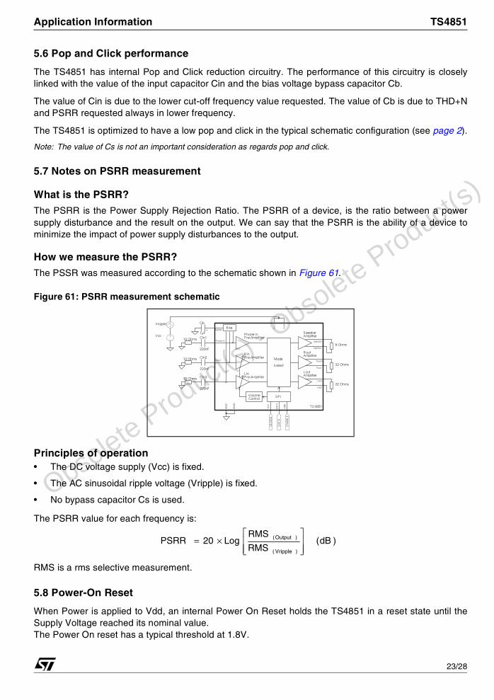
How we measure the PSRR?
The PSSR was measured according to the schematic shown in Figure 61.
Figure 61: PSRR measurement schematic
Principles of operation• The DC voltage supply (Vcc) is fixed.
• The AC sinusoidal ripple voltage (Vripple) is fixed.
• No bypass capacitor Cs is used.
The PSRR value for each frequency is:
RMS is a rms selective measurement.
5.8 Power-On Reset
When Power is applied to Vdd, an internal Power On Reset holds the TS4851 in a reset state until theSupply Voltage reached its nominal value.The Power On reset has a typical threshold at 1.8V.
)dB(RMS
RMSLog20PSRR
)Vripple(
)Output(
⎥⎥⎦
⎤
⎢⎢⎣
⎡×=
Obso
lete Product(s)
- Obso
lete Product(s)
23/28
TS4851 Package Information
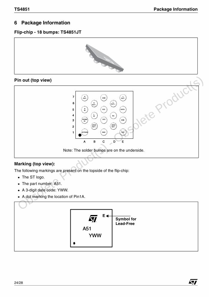
6 Package Information
Flip-chip - 18 bumps: TS4851JT
Pin out (top view)
Marking (top view):
The following markings are present on the topside of the flip-chip:
The ST logo.
The part number: A51.
A 3-digit date code: YWW.
A dot marking the location of Pin1A.
Note: The solder bumps are on the underside.
ROUT- GND
ROUT +
LOUT -
LOUT +
RIN
VCC DATA
LIN
VCC
NC
ENBPHONEIN
SPKROUT +
SPKROUT -
CLKGNDBYPASS1
5
4
3
2
7
6
A EDCB
ROUT- GND
ROUT +
LOUT -
LOUT +
RIN
VCC DATA
LIN
VCC
NC
ENBPHONEIN
SPKROUT +
SPKROUT -
CLKGNDBYPASS1
5
4
3
2
7
6
A EDCB
A51YWW
A51YWW
ESymbol forLead-Free
Obso
lete Product(s)
- Obso
lete Product(s)
24/28
Package Information TS4851
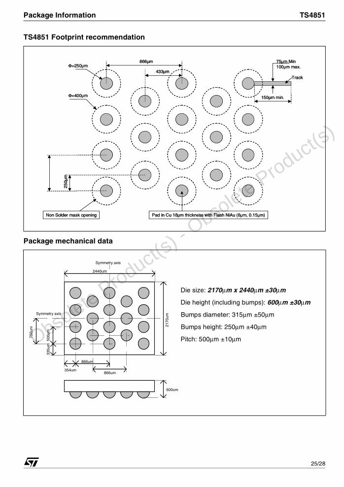
TS4851 Footprint recommendation
Package mechanical data
Pad in Cu 18µm thickness with Flash NiAu (6µm, 0.15µm)
150µm min.
433µm 25
0µm
866µm
Φ=250µm
Φ=400µm
75µm Min100µm max.
Track
Non Solder mask opening Pad in Cu 18µm thickness with Flash NiAu (6µm, 0.15µm)
150µm min.
433µm 25
0µm
866µm
Φ=250µm
Φ=400µm
75µm Min100µm max.
Track
Non Solder mask opening
750u
m
500u
m33
5um
354um
866um
866um
2440um
2170
um
Symmetry axis
Symmetry axis
600um
Die size: 2170µm x 2440µm ±30µm
Die height (including bumps): 600µm ±30µm
Bumps diameter: 315µm ±50µm
Bumps height: 250µm ±40µm
Pitch: 500µm ±10µm
Obso
lete Product(s)
- Obso
lete Product(s)
25/28
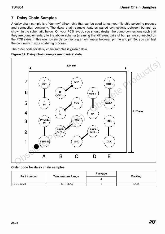
TS4851 Daisy Chain Samples
7 Daisy Chain SamplesA daisy chain sample is a “dummy” silicon chip that can be used to test your flip-chip soldering processand connection continuity. The daisy chain sample features paired connections between bumps, asshown in the schematic below. On your PCB layout, you should design the bump connections such thatthey are complementary to the above schema (meaning that different pairs of bumps are connected onthe PCB side). In this way, by simply connecting an ohmmeter between pin 1A and pin 5A, you can testthe continuity of your soldering process.
The order code for daisy chain samples is given below.
Order code for daisy chain samples
Figure 62: Daisy chain sample mechanical data
ROUT-
GND
ROUT +
LOUT -
LOUT +
RIN
VCC DATA
LIN
VCC
NC
ENBPHONEIN
SPKROUT +
SPKROUT -
CLKGNDBYPASS
2.44 mm
2.17 mm
A EDCB
1
5
4
3
2
7
6
ROUT-
GND
ROUT +
LOUT -
LOUT +
RIN
VCC DATA
LIN
VCC
NC
ENBPHONEIN
SPKROUT +
SPKROUT -
CLKGNDBYPASS
2.44 mm
2.17 mm
ROUT-
GND
ROUT +
LOUT -
LOUT +
RIN
VCC DATA
LIN
VCC
NC
ENBPHONEIN
SPKROUT +
SPKROUT -
CLKGNDBYPASS
ROUT-
GND
ROUT +
LOUT -
LOUT +
RIN
VCC DATA
LIN
VCC
NC
ENBPHONEIN
SPKROUT +
SPKROUT -
CLKGNDBYPASS
ROUT-
GND
ROUT +
LOUT -
LOUT +
RIN
VCC DATA
LIN
VCC
NC
ENBPHONEIN
SPKROUT +
SPKROUT -
CLKGNDBYPASS
2.44 mm
2.17 mm
A EDCB
1
5
4
3
2
7
6
A EDCB
1
5
4
3
2
7
6
Part Number Temperature RangePackage
MarkingJ
TSDC02IJT -40, +85°C • DC2
Obso
lete Product(s)
- Obso
lete Product(s)
26/28
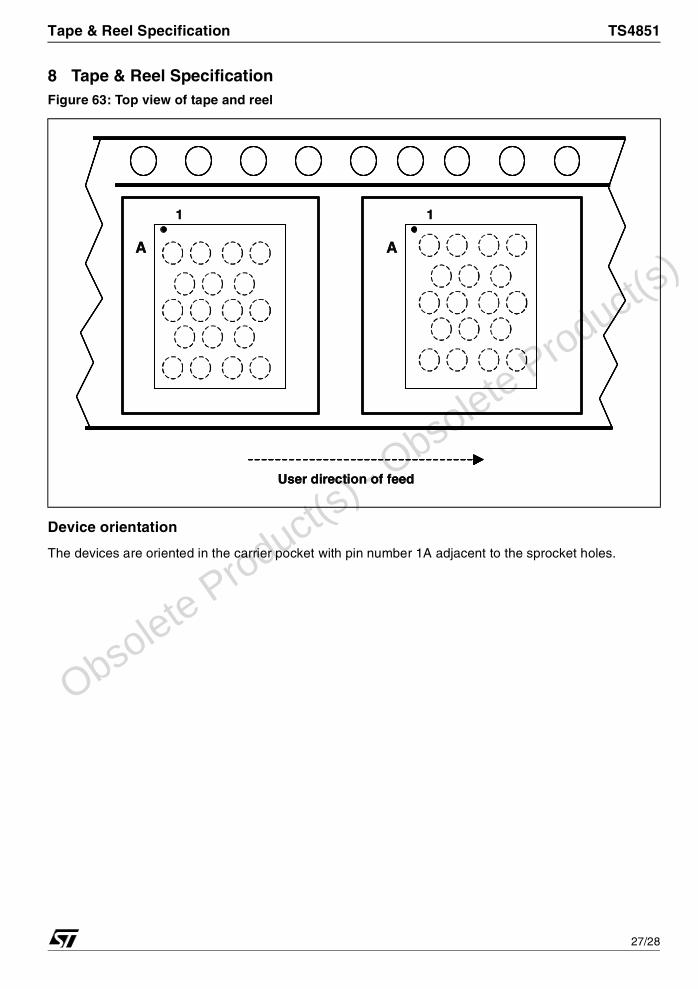
Tape & Reel Specification TS4851
8 Tape & Reel Specification
Device orientation
The devices are oriented in the carrier pocket with pin number 1A adjacent to the sprocket holes.
Figure 63: Top view of tape and reel
A
1
A
1
User direction of feed
A
1
A
1
User direction of feed
Obso
lete Product(s)
- Obso
lete Product(s)
27/28
TS4851 Revision History
9 Revision History
Date Revision Description of Changes
01 July 2002 1 First Release
01 April 2003 2 Curves inserted in the document
01 April 2004 3 Curves updated in the document
01 Jan. 2005 4 Leadfree codification added in the document
01 March 2005 5 Realignment of curve data in the document
Information furnished is bel ieved to be accurate and rel iab le. However, STMicroelectronics assumes no responsibil ity for the consequencesof use o f such information nor for any infringement of patents or other righ ts of third parti es which may result from its use. No license is grantedby implica ti on or o therwise under any patent or patent rights o f STMicroelectronics. Speci fications mentioned in th is pub lica tion are subjectto change without notice. Th is pub lica ti on supersedes and replaces a ll in formation previously suppli ed. STMicroelectronics products are notauthorized for use as critical components in li fe support devices or systems without express wri tten approval of STMicroelectronics.
The ST logo is a registered trademark of STMicroe lectronicsAl l other names are the property of the ir respective owners
© 2005 STMicroelectronics - All rights reserved
STMicroelectronics group o f companiesAustra lia - Belgium - Brazi l - Canada - China - Czech Republic - Finland - France - Germany - Hong Kong - Ind ia - Israel - Italy - Japan -
Malaysia - Mal ta - Morocco - Singapore - Spa in - Sweden - Switzerland - United Kingdom - Un ited States of Americawww.st.com
Obso
lete Product(s)
- Obso
lete Product(s)
28/28