
DIGITAL AMPLIFIER POWER STAGE - Texas Instruments · TAS5112A SLES094B - OCTOBER 2003 - REVISED...
30
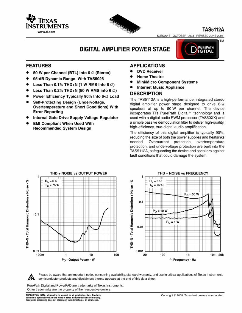
TAS5112A SLES094B - OCTOBER 2003 - REVISED JUNE 2008 DIGITAL AMPLIFIER POWER STAGE TM FEATURES D 50 W per Channel (BTL) Into 6 Ω (Stereo) D 95-dB Dynamic Range With TAS5026 D Less Than 0.1% THD+N (1 W RMS Into 6 Ω) D Less Than 0.2% THD+N (50 W RMS into 6 Ω) D Power Efficiency Typically 90% Into 6-Ω Load D Self-Protecting Design (Undervoltage, Overtemperature and Short Conditions) With Error Reporting D Internal Gate Drive Supply Voltage Regulator D EMI Compliant When Used With Recommended System Design APPLICATIONS D DVD Receiver D Home Theatre D Mini/Micro Component Systems D Internet Music Appliance DESCRIPTION The TAS5112A is a high-performance, integrated stereo digital amplifier power stage designed to drive 6-Ω speakers at up to 50 W per channel. The device incorporates TI’s PurePath Digitalt technology and is used with a digital audio PWM processor (TAS50XX) and a simple passive demodulation filter to deliver high-quality, high-efficiency, true-digital audio amplification. The efficiency of this digital amplifier is typically 90%, reducing the size of both the power supplies and heatsinks needed. Overcurrent protection, overtemperature protection, and undervoltage protection are built into the TAS5112A, safeguarding the device and speakers against fault conditions that could damage the system. P O - Output Power - W 100m R L = 6 Ω T C = 75°C 1 10 100 0.01 0.1 1 THD+N - Total Harmonic Distortion + Noise - % THD + NOISE vs OUTPUT POWER f - Frequency - Hz 20 100 1k 10k THD+N - Total Harmonic Distortion + Noise - % 0.001 0.1 1 20k R L = 6 Ω T C = 75°C 0.01 THD + NOISE vs FREQUENCY P O = 50 W P O = 1 W P O = 10 W PurePath Digital and PowerPAD are trademarks of Texas Instruments. Other trademarks are the property of their respective owners. PRODUCTION DATA information is current as of publication date. Products conform to specifications per the terms of Texas Instruments standard warranty. Production processing does not necessarily include testing of all parameters. Please be aware that an important notice concerning availability, standard warranty, and use in critical applications of Texas Instruments semiconductor products and disclaimers thereto appears at the end of this data sheet. www.ti.com Copyright © 2008, Texas Instruments Incorporated
Transcript of DIGITAL AMPLIFIER POWER STAGE - Texas Instruments · TAS5112A SLES094B - OCTOBER 2003 - REVISED...
TAS5112ASLES094B - OCTOBER 2003 - REVISED JUNE 2008
DIGITAL AMPLIFIER POWER STAGE
TM
FEATURES 50 W per Channel (BTL) Into 6 Ω (Stereo)
95-dB Dynamic Range With TAS5026
Less Than 0.1% THD+N (1 W RMS Into 6 Ω)
Less Than 0.2% THD+N (50 W RMS into 6 Ω)
Power Efficiency Typically 90% Into 6-Ω Load
Self-Protecting Design (Undervoltage,Overtemperature and Short Conditions) WithError Reporting
Internal Gate Drive Supply Voltage Regulator
EMI Compliant When Used WithRecommended System Design
APPLICATIONS DVD Receiver Home Theatre Mini/Micro Component Systems Internet Music Appliance
DESCRIPTIONThe TAS5112A is a high-performance, integrated stereodigital amplifier power stage designed to drive 6-Ωspeakers at up to 50 W per channel. The deviceincorporates TI’s PurePath Digital technology and isused with a digital audio PWM processor (TAS50XX) anda simple passive demodulation filter to deliver high-quality,high-efficiency, true-digital audio amplification.
The efficiency of this digital amplifier is typically 90%,reducing the size of both the power supplies and heatsinksneeded. Overcurrent protection, overtemperatureprotection, and undervoltage protection are built into theTAS5112A, safeguarding the device and speakers againstfault conditions that could damage the system.
PO - Output Power - W
100m
RL = 6 ΩTC = 75°C
1 10 1000.01
0.1
1
TH
D+N
- To
tal H
arm
on
ic D
isto
rtio
n +
No
ise
- %
THD + NOISE vs OUTPUT POWER
f - Frequency - Hz
20 100 1k 10k
TH
D+N
- To
tal H
arm
on
ic D
isto
rtio
n +
No
ise
- %
0.001
0.1
1
20k
RL = 6 ΩTC = 75°C
0.01
THD + NOISE vs FREQUENCY
PO = 50 W
PO = 1 W
PO = 10 W
PurePath Digital and PowerPAD are trademarks of Texas Instruments.Other trademarks are the property of their respective owners.
PRODUCTION DATA information is current as of publication date. Productsconform to specifications per the terms of Texas Instruments standard warranty.Production processing does not necessarily include testing of all parameters.
Please be aware that an important notice concerning availability, standard warranty, and use in critical applications of Texas Instrumentssemiconductor products and disclaimers thereto appears at the end of this data sheet.
www.ti.com
Copyright © 2008, Texas Instruments Incorporated
TAS5112ASLES094B - OCTOBER 2003 - REVISED JUNE 2008
www.ti.com
2
These devices have limited built-in ESD protection. The leads should be shorted together or the device placed in conductive foam duringstorage or handling to prevent electrostatic damage to the MOS gates.
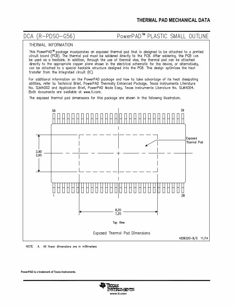
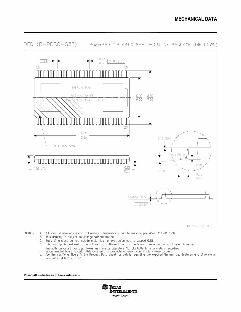
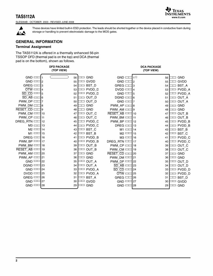
GENERAL INFORMATIONTerminal Assignment
The TAS5112A is offered in a thermally enhanced 56-pinTSSOP DFD (thermal pad is on the top) and DCA (thermalpad is on the bottom), shown as follows.
12345678910111213141516171819202122232425262728
56555453525150494847464544434241403938373635343332313029
GNDGND
GREGOTW
SD_CDSD_AB
PWM_DPPWM_DM
RESET_CDPWM_CMPWM_CP
DREG_RTNM3M2M1
DREGPWM_BPPWM_BM
RESET_ABPWM_AMPWM_AP
GNDDGND
GNDDVDDGREG
GNDGND
GNDGVDDBST_DPVDD_DPVDD_DOUT_DOUT_DGNDGNDOUT_COUT_CPVDD_CPVDD_CBST_CBST_BPVDD_BPVDD_BOUT_BOUT_BGNDGNDOUT_AOUT_APVDD_APVDD_ABST_AGVDDGND
DFD PACKAGE(TOP VIEW)
12345678910111213141516171819202122232425262728
56555453525150494847464544434241403938373635343332313029
GNDGND
GREGDVDD
GNDDGND
GNDPWM_APPWM_AM
RESET_ABPWM_BMPWM_BP
DREGM1M2M3
DREG_RTNPWM_CPPWM_CM
RESET_CDPWM_DMPWM_DP
SD_ABSD_CD
OTWGREG
GNDGND
GNDGVDDBST_APVDD_APVDD_AOUT_AOUT_AGNDGNDOUT_BOUT_BPVDD_BPVDD_BBST_BBST_CPVDD_CPVDD_COUT_COUT_CGNDGNDOUT_DOUT_DPVDD_DPVDD_DBST_DGVDDGND
DCA PACKAGE(TOP VIEW)
TAS5112ASLES094B - OCTOBER 2003 - REVISED JUNE 2008
www.ti.com
3
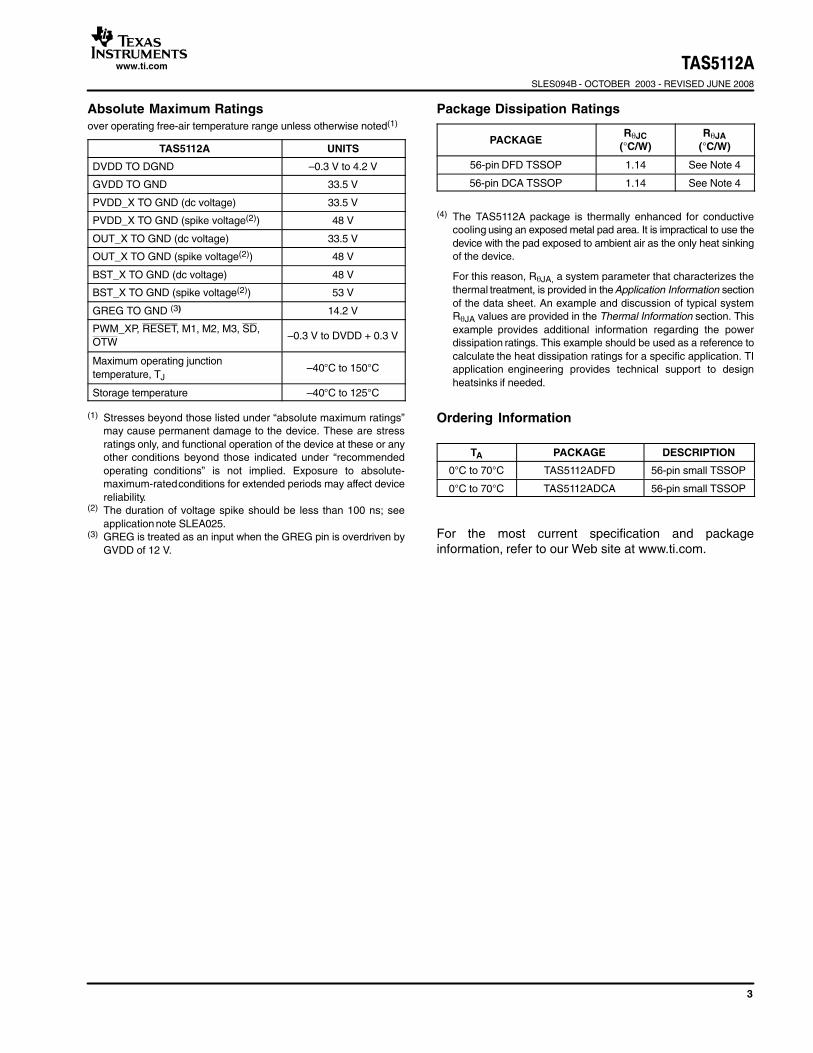
Absolute Maximum Ratingsover operating free-air temperature range unless otherwise noted(1)
TAS5112A UNITS
DVDD TO DGND –0.3 V to 4.2 V
GVDD TO GND 33.5 V
PVDD_X TO GND (dc voltage) 33.5 V
PVDD_X TO GND (spike voltage(2)) 48 V
OUT_X TO GND (dc voltage) 33.5 V
OUT_X TO GND (spike voltage(2)) 48 V
BST_X TO GND (dc voltage) 48 V
BST_X TO GND (spike voltage(2)) 53 V
GREG TO GND (3) 14.2 V
PWM_XP, RESET, M1, M2, M3, SD,OTW
–0.3 V to DVDD + 0.3 V
Maximum operating junctiontemperature, TJ
–40°C to 150°C
Storage temperature –40°C to 125°C
(1) Stresses beyond those listed under “absolute maximum ratings”may cause permanent damage to the device. These are stressratings only, and functional operation of the device at these or anyother conditions beyond those indicated under “recommendedoperating conditions” is not implied. Exposure to absolute-maximum-rated conditions for extended periods may affect devicereliability.
(2) The duration of voltage spike should be less than 100 ns; seeapplication note SLEA025.
(3) GREG is treated as an input when the GREG pin is overdriven byGVDD of 12 V.
Package Dissipation Ratings
PACKAGERθJC
(°C/W)RθJA
(°C/W)
56-pin DFD TSSOP 1.14 See Note 4
56-pin DCA TSSOP 1.14 See Note 4
(4) The TAS5112A package is thermally enhanced for conductivecooling using an exposed metal pad area. It is impractical to use thedevice with the pad exposed to ambient air as the only heat sinkingof the device.
For this reason, RθJA, a system parameter that characterizes thethermal treatment, is provided in the Application Information sectionof the data sheet. An example and discussion of typical systemRθJA values are provided in the Thermal Information section. Thisexample provides additional information regarding the powerdissipation ratings. This example should be used as a reference tocalculate the heat dissipation ratings for a specific application. TIapplication engineering provides technical support to designheatsinks if needed.
Ordering Information
TA PACKAGE DESCRIPTION
0°C to 70°C TAS5112ADFD 56-pin small TSSOP
0°C to 70°C TAS5112ADCA 56-pin small TSSOP
For the most current specification and packageinformation, refer to our Web site at www.ti.com.
TAS5112ASLES094B - OCTOBER 2003 - REVISED JUNE 2008
www.ti.com
4
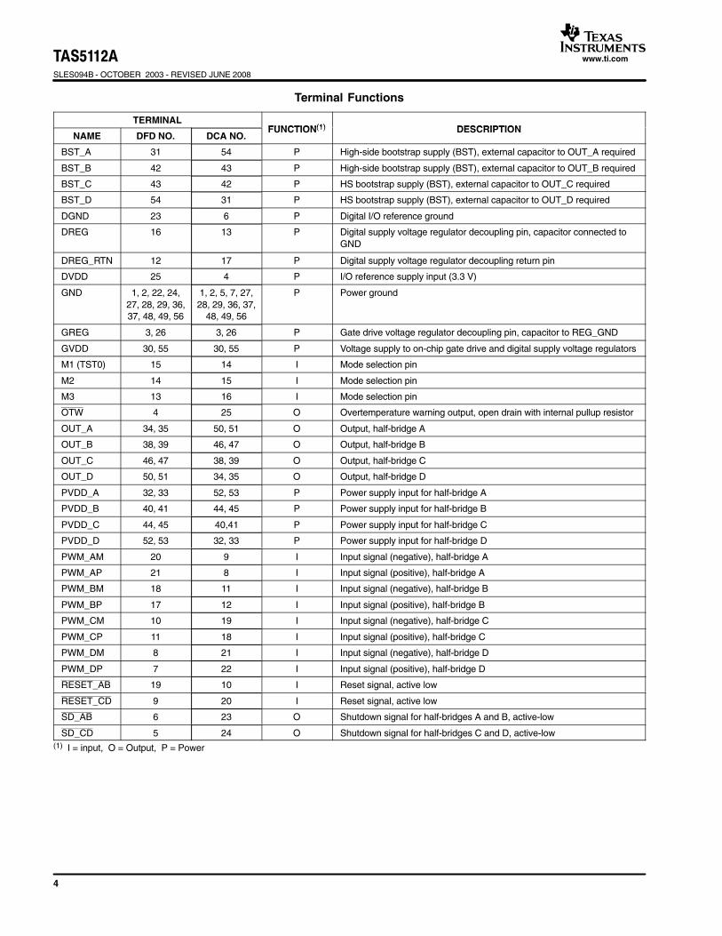
Terminal Functions
TERMINALFUNCTION(1) DESCRIPTION
NAME DFD NO. DCA NO.FUNCTION(1) DESCRIPTION
BST_A 31 54 P High-side bootstrap supply (BST), external capacitor to OUT_A required
BST_B 42 43 P High-side bootstrap supply (BST), external capacitor to OUT_B required
BST_C 43 42 P HS bootstrap supply (BST), external capacitor to OUT_C required
BST_D 54 31 P HS bootstrap supply (BST), external capacitor to OUT_D required
DGND 23 6 P Digital I/O reference ground
DREG 16 13 P Digital supply voltage regulator decoupling pin, capacitor connected toGND
DREG_RTN 12 17 P Digital supply voltage regulator decoupling return pin
DVDD 25 4 P I/O reference supply input (3.3 V)
GND 1, 2, 22, 24,27, 28, 29, 36,37, 48, 49, 56
1, 2, 5, 7, 27,28, 29, 36, 37,
48, 49, 56
P Power ground
GREG 3, 26 3, 26 P Gate drive voltage regulator decoupling pin, capacitor to REG_GND
GVDD 30, 55 30, 55 P Voltage supply to on-chip gate drive and digital supply voltage regulators
M1 (TST0) 15 14 I Mode selection pin
M2 14 15 I Mode selection pin
M3 13 16 I Mode selection pin
OTW 4 25 O Overtemperature warning output, open drain with internal pullup resistor
OUT_A 34, 35 50, 51 O Output, half-bridge A
OUT_B 38, 39 46, 47 O Output, half-bridge B
OUT_C 46, 47 38, 39 O Output, half-bridge C
OUT_D 50, 51 34, 35 O Output, half-bridge D
PVDD_A 32, 33 52, 53 P Power supply input for half-bridge A
PVDD_B 40, 41 44, 45 P Power supply input for half-bridge B
PVDD_C 44, 45 40,41 P Power supply input for half-bridge C
PVDD_D 52, 53 32, 33 P Power supply input for half-bridge D
PWM_AM 20 9 I Input signal (negative), half-bridge A
PWM_AP 21 8 I Input signal (positive), half-bridge A
PWM_BM 18 11 I Input signal (negative), half-bridge B
PWM_BP 17 12 I Input signal (positive), half-bridge B
PWM_CM 10 19 I Input signal (negative), half-bridge C
PWM_CP 11 18 I Input signal (positive), half-bridge C
PWM_DM 8 21 I Input signal (negative), half-bridge D
PWM_DP 7 22 I Input signal (positive), half-bridge D
RESET_AB 19 10 I Reset signal, active low
RESET_CD 9 20 I Reset signal, active low
SD_AB 6 23 O Shutdown signal for half-bridges A and B, active-low
SD_CD 5 24 O Shutdown signal for half-bridges C and D, active-low(1) I = input, O = Output, P = Power
TAS5112ASLES094B - OCTOBER 2003 - REVISED JUNE 2008
www.ti.com
5
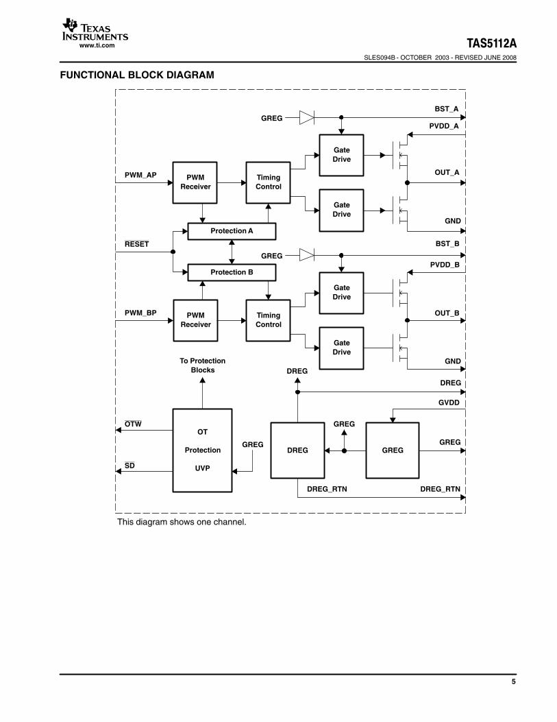
FUNCTIONAL BLOCK DIAGRAM
GREG
GVDD
GREG
DREG_RTN
TimingControl
GateDrive
PWM_AP OUT_A
GND
PVDD_A
BST_A
PWMReceiver
OUT_B
GND
PVDD_BGREG
Protection A
Protection B
PWM_BP
RESET
GREG
BST_B
DREG
To ProtectionBlocks
OTW
SD
DREG
DREG_RTN
GREG
DREG
GateDrive
GateDrive
GateDrive
GREG
OT
Protection
UVP
PWMReceiver
TimingControl
This diagram shows one channel.
TAS5112ASLES094B - OCTOBER 2003 - REVISED JUNE 2008
www.ti.com
6
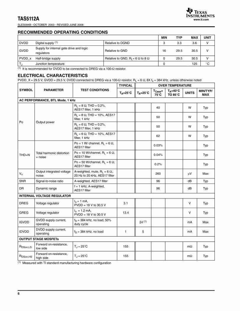
RECOMMENDED OPERATING CONDITIONSMIN TYP MAX UNIT
DVDD Digital supply (1) Relative to DGND 3 3.3 3.6 V
GVDDSupply for internal gate drive and logic
regulatorsRelative to GND 16 29.5 30.5 V
PVDD_x Half-bridge supply Relative to GND, RL= 6 Ω to 8 Ω 0 29.5 30.5 V
TJ Junction temperature 0 125 C(1) It is recommended for DVDD to be connected to DREG via a 100-Ω resistor.
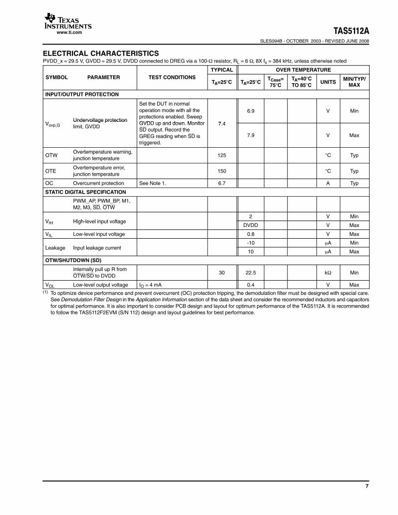
ELECTRICAL CHARACTERISTICSPVDD_X = 29.5 V, GVDD = 29.5 V, DVDD connected to DREG via a 100-Ω resistor, RL = 6 Ω, 8X fs = 384 kHz, unless otherwise noted
TYPICAL OVER TEMPERATURESYMBOL PARAMETER TEST CONDITIONS
TA=25°C TA=25°CTCase=75°C
TA=40°CTO 85°C
UNITSMIN/TYP/
MAX
AC PERFORMANCE, BTL Mode, 1 kHz
RL = 8 Ω, THD = 0.2%,AES17 filter, 1 kHz
40 W Typ
Po Output power
RL = 8 Ω, THD = 10%, AES17filter, 1 kHz
50 W Typ
Po Output powerRL = 6 Ω, THD = 0.2%,AES17 filter, 1 kHz
50 W Typ
RL = 6 Ω, THD = 10%, AES17filter, 1 kHz
62 W Typ
Po = 1 W/ channel, RL = 6 Ω,AES17 filter
0.03% Typ
THD+NTotal harmonic distortion+ noise
Po = 10 W/channel, RL = 6 Ω,AES17 filter
0.04% Typ+ noise
Po = 50 W/channel, RL = 6 Ω,AES17 filter
0.2% Typ
VnOutput integrated voltagenoise
A-weighted, mute, RL = 6 Ω,,20 Hz to 20 kHz, AES17 filter
260 µV Max
SNR Signal-to-noise ratio A-weighted, AES17 filter 96 dB Typ
DR Dynamic rangef = 1 kHz, A-weighted,AES17 filter
96 dB Typ
INTERNAL VOLTAGE REGULATOR
DREG Voltage regulatorIo = 1 mA,PVDD = 18 V to 30.5 V
3.1 V Typ
GREG Voltage regulatorIo = 1.2 mA,PVDD = 18 V to 30.5 V
13.4 V Typ
IGVDDGVDD supply current,operating
fS = 384 kHz, no load, 50%duty cycle
24 (1) mA Max
IDVDDDVDD supply current,operating
fS = 384 kHz, no load 1 5 mA Max
OUTPUT STAGE MOSFETs
RDSon,LSForward on-resistance,low side
TJ = 25°C 155 mΩ Typ
RDSon,HSForward on-resistance,high side
TJ = 25°C 155 mΩ Typ
(1) Measured with TI standard manufacturing hardware configuration
TAS5112ASLES094B - OCTOBER 2003 - REVISED JUNE 2008
www.ti.com
7
ELECTRICAL CHARACTERISTICSPVDD_x = 29.5 V, GVDD = 29.5 V, DVDD connected to DREG via a 100-Ω resistor, RL = 6 Ω, 8X fs = 384 kHz, unless otherwise noted
TYPICAL OVER TEMPERATURESYMBOL PARAMETER TEST CONDITIONS
TA=25°C TA=25°CTCase=75°C
TA=40°CTO 85°C
UNITSMIN/TYP/
MAX
INPUT/OUTPUT PROTECTION
VUndervoltage protection
Set the DUT in normaloperation mode with all theprotections enabled. SweepGVDD up and down Monitor 7 4
6.9 V Min
Vuvp,GUndervoltage protectionlimit, GVDD
GVDD up and down. MonitorSD output. Record theGREG reading when SD istriggered.
7.4
7.9 V Max
OTWOvertemperature warning,junction temperature
125 °C Typ
OTEOvertemperature error,junction temperature
150 °C Typ
OC Overcurrent protection See Note 1. 6.7 A Typ
STATIC DIGITAL SPECIFICATION
PWM_AP, PWM_BP, M1,M2, M3, SD, OTW
V High level input voltage2 V Min
VIH High-level input voltageDVDD V Max
VIL Low-level input voltage 0.8 V Max
L k I t l k t-10 µA Min
Leakage Input leakage current10 µA Max
OTW/SHUTDOWN (SD)
Internally pull up R fromOTW/SD to DVDD
30 22.5 kΩ Min
VOL Low-level output voltage IO = 4 mA 0.4 V Max(1) To optimize device performance and prevent overcurrent (OC) protection tripping, the demodulation filter must be designed with special care.
See Demodulation Filter Design in the Application Information section of the data sheet and consider the recommended inductors and capacitorsfor optimal performance. It is also important to consider PCB design and layout for optimum performance of the TAS5112A. It is recommendedto follow the TAS5112F2EVM (S/N 112) design and layout guidelines for best performance.
TAS5112ASLES094B - OCTOBER 2003 - REVISED JUNE 2008
www.ti.com
8
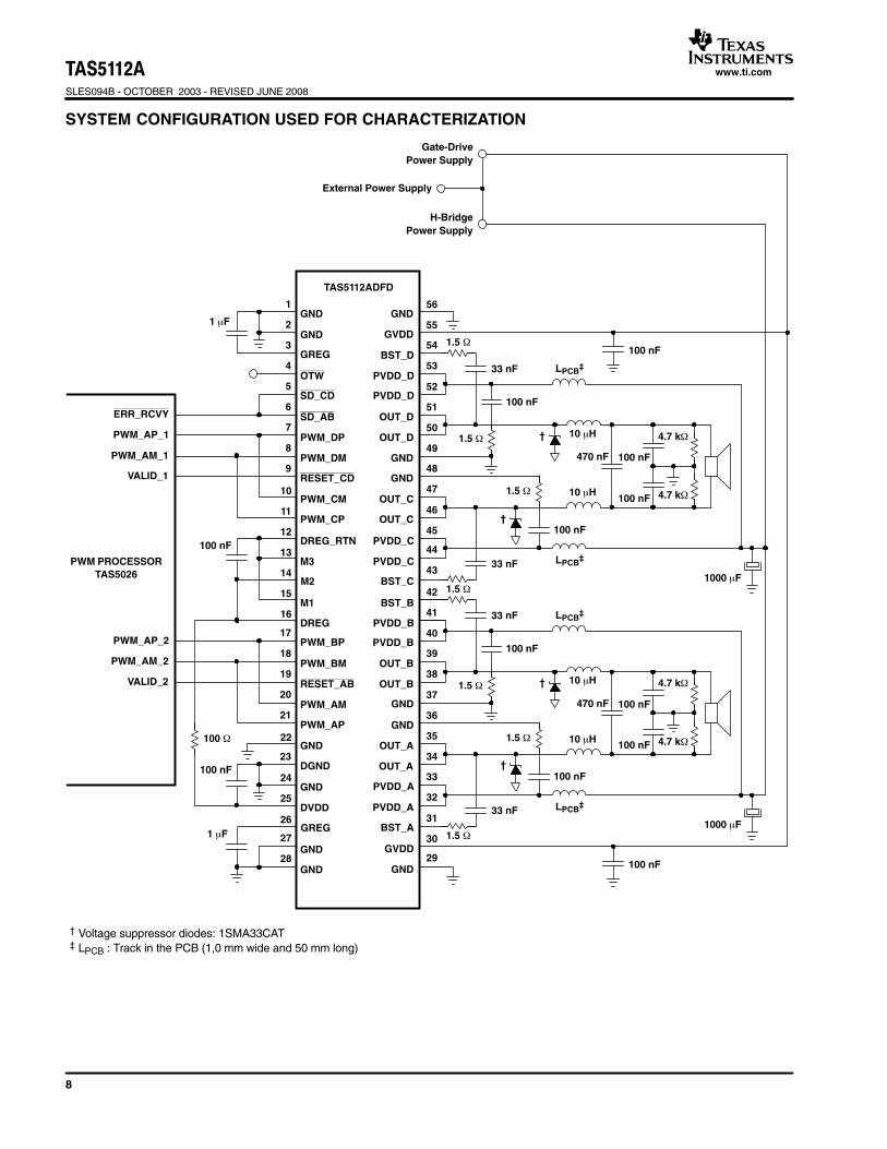
SYSTEM CONFIGURATION USED FOR CHARACTERIZATION
TAS5112ADFD
VALID_1
42
41
4
13
11
10
9
8
7
PWM PROCESSORTAS5026
GVDD
OUT_C
BST_D
PVDD_C
GND
PVDD_D
PVDD_D
PVDD_C
OUT_D
52
53
55
OUT_D
54
GND
OUT_C
56
51
49
47
50
48
BST_C
BST_B
PVDD_B
44
46
43
45
6
14
15
16
12
5
1
2
3
10 µH
10 µH
470 nF
4.7 kΩ
1000 µF
100 nF
PWM_AP_1
PWM_AM_1 100 nF
100 nF
1.5 Ω
100 nF
33 nF
H-BridgePower Supply
Gate-DrivePower Supply
External Power Supply
4.7 kΩ
LPCB‡
DREG
SD_CD
M1
PWM_CM
RESET_CD
PWM_DP
SD_AB
PWM_DM
GREG
M2
M3
DREG_RTN
PWM_CP
OTW
GND
GND GND
LPCB‡
33 nF
100 nF
1.5 Ω
PVDD_B
PVDD_A
OUT_B
GND
OUT_A
GND
OUT_B
GVDD
OUT_A
GND
PVDD_A
BST_A
37
38
40
39
36
34
32
35
33
29
31
30
10 µH
10 µH
470 nF
4.7 kΩ
1000 µF
100 nF
100 nF
1.5 Ω
100 nF
33 nF
4.7 kΩ
LPCB‡
LPCB‡
33 nF
100 nF
1.5 Ω
100 nFGND
PWM_BP
GND
GND
PWM_AP
RESET_AB
PWM_BM
PWM_AM
GREG
DVDD
GND
DGND
25
23
22
21
20
19
18
26
27
28
24
17
1 µF
ERR_RCVY
100 nF
VALID_2
PWM_AP_2
PWM_AM_2
100 Ω
100 nF
1 µF
1.5 Ω
1.5 Ω
1.5 Ω
† Voltage suppressor diodes: 1SMA33CAT‡ LPCB : Track in the PCB (1,0 mm wide and 50 mm long)
†
†
†
†
TAS5112ASLES094B - OCTOBER 2003 - REVISED JUNE 2008
www.ti.com
9
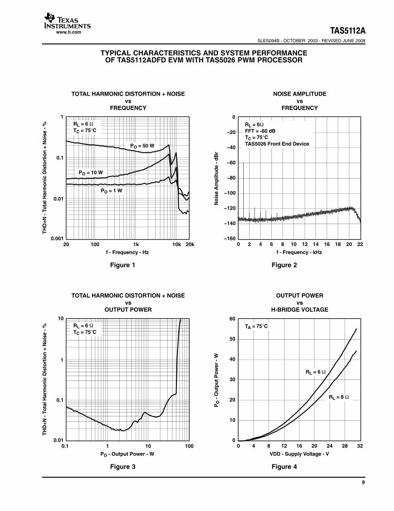
TYPICAL CHARACTERISTICS AND SYSTEM PERFORMANCEOF TAS5112ADFD EVM WITH TAS5026 PWM PROCESSOR
Figure 1
f - Frequency - Hz
20 100 1k 10k
TH
D+N
- To
tal H
arm
on
ic D
isto
rtio
n +
No
ise
- %
TOTAL HARMONIC DISTORTION + NOISEvs
FREQUENCY
0.001
0.1
1
20k
RL = 6 ΩTC = 75°C
0.01
PO = 50 W
PO = 1 W
PO = 10 W
Figure 2
f - Frequency - kHz
−160
−140
−120
−100
−80
−60
−40
−20
0
0 2 4 6 8 10 12 14 16 18 20 22
RL = 6ΩFFT = -60 dBTC = 75°CTAS5026 Front End Device
No
ise
Am
plit
ud
e - d
Br
NOISE AMPLITUDEvs
FREQUENCY
Figure 3
PO - Output Power - W
0.1
RL = 6 ΩTC = 75°C
1 10 100
TH
D+N
- To
tal H
arm
on
ic D
isto
rtio
n +
No
ise
- %
TOTAL HARMONIC DISTORTION + NOISEvs
OUTPUT POWER
0.01
0.1
10
1
Figure 4
VDD - Supply Voltage - V
0
10
20
30
40
50
60
0 4 8 12 16 20 24 28 32
TA = 75°C
PO
- O
utp
ut
Po
wer
- W
OUTPUT POWERvs
H-BRIDGE VOLTAGE
RL = 6 Ω
RL = 8 Ω
TAS5112ASLES094B - OCTOBER 2003 - REVISED JUNE 2008
www.ti.com
10
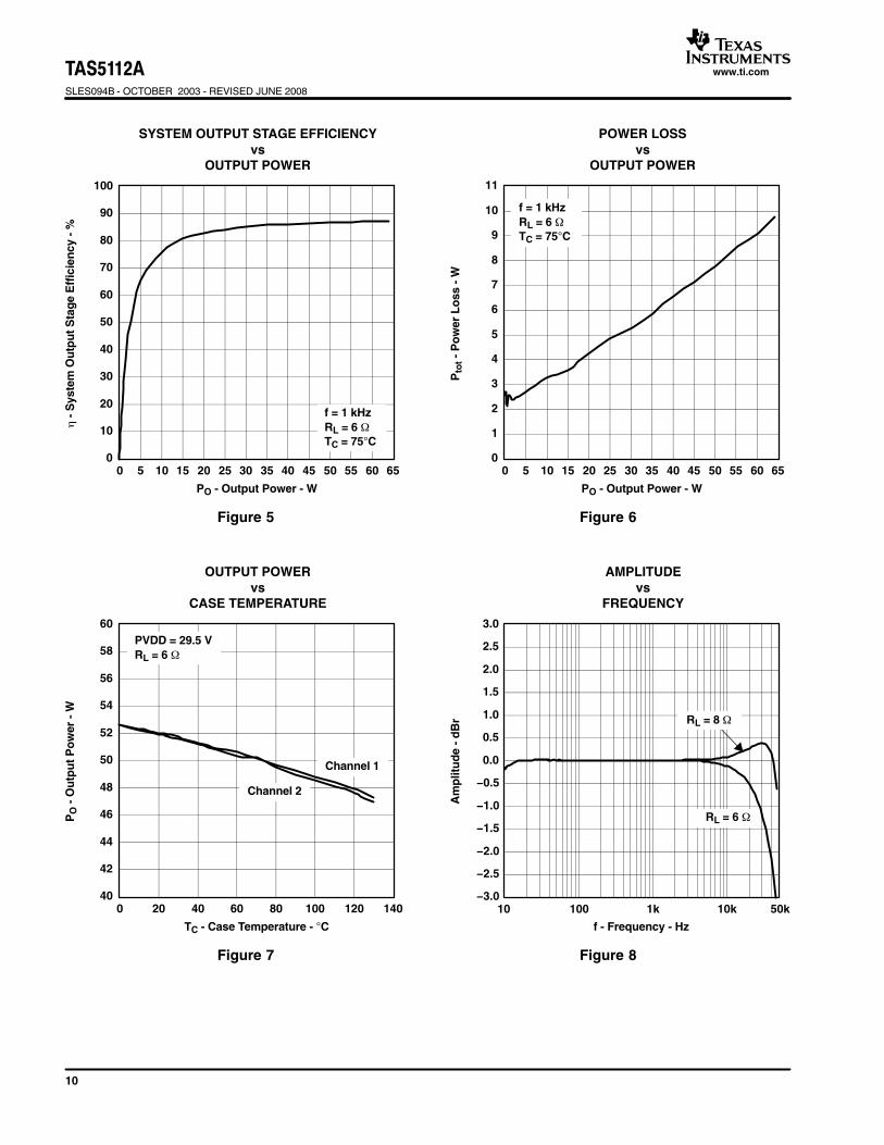
Figure 5
PO - Output Power - W
0
10
20
30
40
50
60
70
80
90
100
0 5 10 15 20 25 30 35 40 45 50 55 60 65
f = 1 kHzRL = 6 ΩTC = 75°C
η -
Sys
tem
Ou
tpu
t Sta
ge
Eff
icie
ncy
- %
SYSTEM OUTPUT STAGE EFFICIENCYvs
OUTPUT POWER
Figure 6
PO - Output Power - W
0
1
2
3
4
5
6
7
8
9
10
11
0 5 10 15 20 25 30 35 40 45 50 55 60 65
f = 1 kHzRL = 6 ΩTC = 75°C
Pto
t - P
ow
er L
oss
- W
POWER LOSSvs
OUTPUT POWER
Figure 7
TC - Case Temperature - °C
40
42
44
46
48
50
52
54
56
58
60
0 20 40 60 80 100 120 140
PVDD = 29.5 VRL = 6 Ω
PO
- O
utp
ut
Po
wer
- W
OUTPUT POWERvs
CASE TEMPERATURE
Channel 1
Channel 2
−3.0
−2.5
−2.0
−1.5
−1.0
−0.5
0.0
0.5
1.0
1.5
2.0
2.5
3.0
f - Frequency - Hz
Am
plit
ud
e - d
Br
10 100 1k 50k10k
Figure 8
RL = 6 Ω
AMPLITUDEvs
FREQUENCY
RL = 8 Ω
TAS5112ASLES094B - OCTOBER 2003 - REVISED JUNE 2008
www.ti.com
11
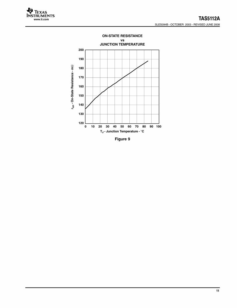
Figure 9
TJ - Junction Temperature - °C
120
130
140
150
160
170
180
190
200
0 10 20 30 40 50 60 70 80 90 100
r on
- On
-Sta
te R
esis
tan
ce -
mΩ
ON-STATE RESISTANCEvs
JUNCTION TEMPERATURE
TAS5112ASLES094B - OCTOBER 2003 - REVISED JUNE 2008
www.ti.com
12
Fro
mP
WM
Pro
cess
or
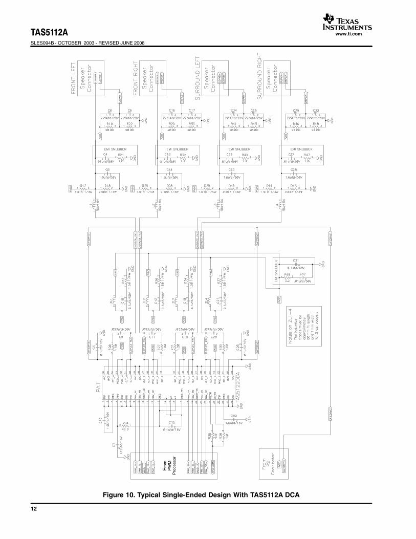
Figure 10. Typical Single-Ended Design With TAS5112A DCA
TAS5112ASLES094B - OCTOBER 2003 - REVISED JUNE 2008
www.ti.com
13
THEORY OF OPERATION
POWER SUPPLIES
The power device only requires two supply voltages,GVDD and PVDD_X.
GVDD is the gate drive supply for the device, regulatedinternally down to approximately 12 V, and decoupled withregards to board GND on the GREG pins through anexternal capacitor. GREG powers both the low side andhigh side via a bootstrap step-up conversion. Thebootstrap supply is charged after the first low-side turn-onpulse. Internal digital core voltage DREG is also derivedfrom GVDD and regulated down by internal circuitry to3.3 V.
The gate-driver regulator can be bypassed for reducingidle loss in the device by shorting GREG to GVDD anddirectly feeding in 12.0 V. This can be useful in anapplication where thermal conduction of heat from thedevice is difficult.
PVDD_X is the H-bridge power supply pin. Two power pinsexists for each half-bridge to handle the current density. Itis important that the circuitry recommendationsconcerning the PVDD_X pins are followed carefully bothtopology- and layout-wise. For topologyrecommendations, see the System Configuration Used forCharacterization section. Following theserecommendations is important for parameters like EMI,reliability, and performance.
POWERING UP
RESET
GVDD
PVDD_X
PWM_xP
> 1 ms> 1 ms
NOTE: PVDD should not be powered up before GVDD.
During power up when RESET is asserted LOW, allMOSFETs are turned off and the two internal half-bridgesare in the high-impedance state (Hi-Z). The bootstrapcapacitors supplying high-side gate drive are not chargedat this point. To comply with the click and pop scheme anduse of non-TI modulators, it is recommended to use a
4.7-kΩ pulldown resistor on each PWM output node toground. This precharges the bootstrap supply capacitorsand discharges the output filter capacitor.
After GVDD has been applied, it takes approximately 800µs to fully charge the BST capacitor. Within this time,RESET must be kept low. After approximately 1 ms, theback-end bootstrap capacitor is charged.
RESET can now be released if the modulator is poweredup and streaming valid PWM signals to the back-endPWM_xP. Valid means a switching PWM signal whichcomplies with the frequency and duty cycle ranges statedin the Recommended Operating Conditions.
A constant HIGH dc level on the PWM_xP is not permitted,because it would force the high-side MOSFET ON until iteventually ran out of BST capacitor energy and mightdamage the device.
An unknown state of the PWM output signals from themodulator is illegal and should be avoided, which inpractice means that the PWM processor must be poweredup and initialized before RESET is de-asserted HIGH tothe back end.
POWERING DOWN
For power down of the back end, an opposite approach isnecessary. The RESET must be asserted LOW before thevalid PWM signal is removed.
When PWM processors are used with TI PurePath Digitalamplifiers, the correct timing control of RESET andPWM_xP is performed by the modulator.
PRECAUTION
The TAS5112A must always start up in thehigh-impedance (Hi-Z) state. In this state, the bootstrap(BST) capacitor is precharged by a resistor on each PWMoutput node to ground. See the system configuration. Thisensures that the back end is ready for receiving PWMpulses, indicating either HIGH- or LOW-side turnon afterRESET is de-asserted to the back end.
With the following pulldown resistor and BST capacitorsize, the charge time is:
C = 33 nF, R = 4.7 kΩR × C × 5 = 775.5 µs
After GVDD has been applied, it takes approximately 800µs to fully charge the BST capacitor. During this time,RESET must be kept low. After approximately 1 ms theback end BST is charged and ready. RESET can now bereleased if the PWM modulator is ready and is streamingvalid PWM signals to the back end. Valid PWM signals areswitching PWM signals with a frequency between350–400 kHz. A constant HIGH level on the PWM+ wouldforce the high-side MOSFET ON until it eventually ran outof BST capacitor energy. Putting the device in thiscondition should be avoided.
TAS5112ASLES094B - OCTOBER 2003 - REVISED JUNE 2008
www.ti.com
14
In practice this means that the DVDD-to-PWM processor(front-end) should be stable and initialization should becompleted before RESET is de-asserted to the back end.
CONTROL I/O
Shutdown Pin: SD
The SD pin functions as an output pin and is intended forprotection-mode signaling to, for example, a controller orother front-end device. The pin is open-drain with aninternal pullup resistor to DVDD.
The logic output is, as shown in the following table, acombination of the device state and RESET input:
SD RESET DESCRIPTION
0 0 Reserved
0 1 Device in protection mode, i.e., UV and/or OCand/or OT error
1(2) 0 Device set high-impedance (Hi-Z), SD forced high
1 1 Normal operation(2) SD is pulled high when RESET is asserted low independent
of chip state (i.e., protection mode). This is desirable tomaintain compatibility with some TI PWM front ends.
Temperature Warning Pin: OTW
The OTW pin gives a temperature warning signal whentemperature exceeds the set limit. The pin is of theopen-drain type with an internal pullup resistor to DVDD.
OTW DESCRIPTION
0 Junction temperature higher than 125°C
1 Junction temperature lower than 125°C
Overall Reporting
The SD pin, together with the OTW pin, gives chip stateinformation as described in Table 1.
Table 1. Error Signal Decoding
OTW SD DESCRIPTION
0 0 Overtemperature error (OTE)
0 1 Overtemperature warning (OTW)
1 0 Overcurrent (OC) or undervoltage (UV) error
1 1 Normal operation, no errors/warnings
Chip Protection
The TAS5112A protection function is implemented in aclosed loop with, for example, a system controller and TIPWM processor. The TAS5112A contains three individualsystems protecting the device against error conditions. Allof the error events covered result in the output stage beingset in a high-impedance state (Hi-Z) for maximumprotection of the device and connected equipment.
The device can be recovered by toggling RESET low andthen high, after all errors are cleared.
Overcurrent (OC) Protection
The device has individual forward current protection onboth high-side and low-side power stage FETs. The OCprotection works only with the demodulation filter presentat the output. See Demodulation Filter Design in theApplication Information section of the data sheet for designconstraints.
Overtemperature (OT) Protection
A dual temperature protection system asserts a warningsignal when the device junction temperature exceeds125°C. The OT protection circuit is shared by allhalf-bridges.
Undervoltage (UV) Protection
Undervoltage lockout occurs when GVDD is insufficientfor proper device operation. The UV protection systemprotects the device under power-up and power-downsituations. The UV protection circuits are shared by allhalf-bridges.
Reset Function
The reset has two functions:
Reset is used for re-enabling operation after alatching error event.
Reset is used for disabling output stageswitching (mute function).
The error latch is cleared on the falling edge of reset andnormal operation is resumed when reset goes high.
PROTECTION MODE
Autorecovery (AR) After Errors (PMODE0)
In autorecovery mode (PMODE0) the TAS5112A isself-supported in handling of error situations. All protectionsystems are active, setting the output stage in thehigh-impedance state to protect the output stage andconnected equipment. However, after a short time periodthe device autorecovers, i.e., operation is automaticallyresumed provided that the system is fully operational.
The autorecovery timing is set by counting PWM inputcycles, i.e., the timing is relative to the switching frequency.
The AR system is common to both half-bridges.
TAS5112ASLES094B - OCTOBER 2003 - REVISED JUNE 2008
www.ti.com
15
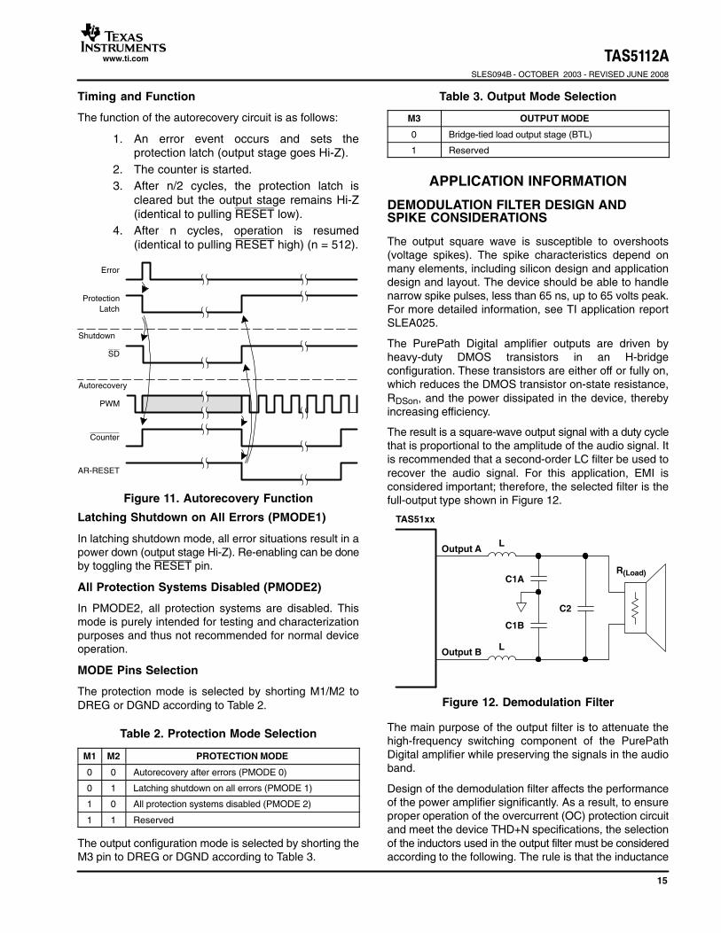
Timing and Function
The function of the autorecovery circuit is as follows:
1. An error event occurs and sets theprotection latch (output stage goes Hi-Z).
2. The counter is started.3. After n/2 cycles, the protection latch is
cleared but the output stage remains Hi-Z(identical to pulling RESET low).
4. After n cycles, operation is resumed(identical to pulling RESET high) (n = 512).
Error
ProtectionLatch
Shutdown
Autorecovery
SD
PWM
Counter
AR-RESET
Figure 11. Autorecovery Function
Latching Shutdown on All Errors (PMODE1)
In latching shutdown mode, all error situations result in apower down (output stage Hi-Z). Re-enabling can be doneby toggling the RESET pin.
All Protection Systems Disabled (PMODE2)
In PMODE2, all protection systems are disabled. Thismode is purely intended for testing and characterizationpurposes and thus not recommended for normal deviceoperation.
MODE Pins Selection
The protection mode is selected by shorting M1/M2 toDREG or DGND according to Table 2.
Table 2. Protection Mode Selection
M1 M2 PROTECTION MODE
0 0 Autorecovery after errors (PMODE 0)
0 1 Latching shutdown on all errors (PMODE 1)
1 0 All protection systems disabled (PMODE 2)
1 1 Reserved
The output configuration mode is selected by shorting theM3 pin to DREG or DGND according to Table 3.
Table 3. Output Mode Selection
M3 OUTPUT MODE
0 Bridge-tied load output stage (BTL)
1 Reserved
APPLICATION INFORMATION
DEMODULATION FILTER DESIGN ANDSPIKE CONSIDERATIONS
The output square wave is susceptible to overshoots(voltage spikes). The spike characteristics depend onmany elements, including silicon design and applicationdesign and layout. The device should be able to handlenarrow spike pulses, less than 65 ns, up to 65 volts peak.For more detailed information, see TI application reportSLEA025.
The PurePath Digital amplifier outputs are driven byheavy-duty DMOS transistors in an H-bridgeconfiguration. These transistors are either off or fully on,which reduces the DMOS transistor on-state resistance,RDSon, and the power dissipated in the device, therebyincreasing efficiency.
The result is a square-wave output signal with a duty cyclethat is proportional to the amplitude of the audio signal. Itis recommended that a second-order LC filter be used torecover the audio signal. For this application, EMI isconsidered important; therefore, the selected filter is thefull-output type shown in Figure 12.
Output A
C1A
TAS51xx
L
Output B L
C1B
C2
R(Load)
Figure 12. Demodulation Filter
The main purpose of the output filter is to attenuate thehigh-frequency switching component of the PurePathDigital amplifier while preserving the signals in the audioband.
Design of the demodulation filter affects the performanceof the power amplifier significantly. As a result, to ensureproper operation of the overcurrent (OC) protection circuitand meet the device THD+N specifications, the selectionof the inductors used in the output filter must be consideredaccording to the following. The rule is that the inductance
TAS5112ASLES094B - OCTOBER 2003 - REVISED JUNE 2008
www.ti.com
16
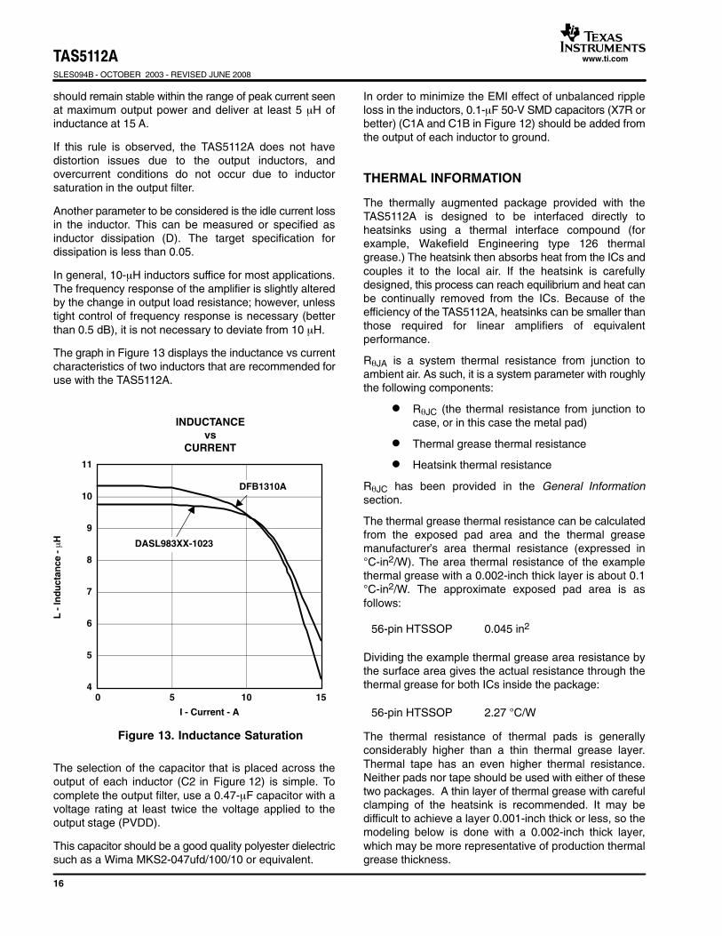
should remain stable within the range of peak current seenat maximum output power and deliver at least 5 µH ofinductance at 15 A.
If this rule is observed, the TAS5112A does not havedistortion issues due to the output inductors, andovercurrent conditions do not occur due to inductorsaturation in the output filter.
Another parameter to be considered is the idle current lossin the inductor. This can be measured or specified asinductor dissipation (D). The target specification fordissipation is less than 0.05.
In general, 10-µH inductors suffice for most applications.The frequency response of the amplifier is slightly alteredby the change in output load resistance; however, unlesstight control of frequency response is necessary (betterthan 0.5 dB), it is not necessary to deviate from 10 µH.
The graph in Figure 13 displays the inductance vs currentcharacteristics of two inductors that are recommended foruse with the TAS5112A.
Figure 13. Inductance Saturation
I - Current - A
4
5
6
7
8
9
10
11
0 5 10 15
L -
Ind
uct
ance
- µ
H
INDUCTANCEvs
CURRENT
DFB1310A
DASL983XX-1023
The selection of the capacitor that is placed across theoutput of each inductor (C2 in Figure 12) is simple. Tocomplete the output filter, use a 0.47-µF capacitor with avoltage rating at least twice the voltage applied to theoutput stage (PVDD).
This capacitor should be a good quality polyester dielectricsuch as a Wima MKS2-047ufd/100/10 or equivalent.
In order to minimize the EMI effect of unbalanced rippleloss in the inductors, 0.1-µF 50-V SMD capacitors (X7R orbetter) (C1A and C1B in Figure 12) should be added fromthe output of each inductor to ground.
THERMAL INFORMATION
The thermally augmented package provided with theTAS5112A is designed to be interfaced directly toheatsinks using a thermal interface compound (forexample, Wakefield Engineering type 126 thermalgrease.) The heatsink then absorbs heat from the ICs andcouples it to the local air. If the heatsink is carefullydesigned, this process can reach equilibrium and heat canbe continually removed from the ICs. Because of theefficiency of the TAS5112A, heatsinks can be smaller thanthose required for linear amplifiers of equivalentperformance.
RθJA is a system thermal resistance from junction toambient air. As such, it is a system parameter with roughlythe following components:
RθJC (the thermal resistance from junction tocase, or in this case the metal pad)
Thermal grease thermal resistance
Heatsink thermal resistance
RθJC has been provided in the General Informationsection.
The thermal grease thermal resistance can be calculatedfrom the exposed pad area and the thermal greasemanufacturer’s area thermal resistance (expressed in°C-in2/W). The area thermal resistance of the examplethermal grease with a 0.002-inch thick layer is about 0.1°C-in2/W. The approximate exposed pad area is asfollows:
56-pin HTSSOP 0.045 in2
Dividing the example thermal grease area resistance bythe surface area gives the actual resistance through thethermal grease for both ICs inside the package:
56-pin HTSSOP 2.27 °C/W
The thermal resistance of thermal pads is generallyconsiderably higher than a thin thermal grease layer.Thermal tape has an even higher thermal resistance.Neither pads nor tape should be used with either of thesetwo packages. A thin layer of thermal grease with carefulclamping of the heatsink is recommended. It may bedifficult to achieve a layer 0.001-inch thick or less, so themodeling below is done with a 0.002-inch thick layer,which may be more representative of production thermalgrease thickness.
TAS5112ASLES094B - OCTOBER 2003 - REVISED JUNE 2008
www.ti.com
17
Heatsink thermal resistance is generally predicted by theheatsink vendor, modeled using a continuous flowdynamics (CFD) model, or measured.
Thus, for a single monaural IC, the system RθJA = RθJC +thermal grease resistance + heatsink resistance.
Table 4, Table 5, and Table 6 indicate modeledparameters for one or two TAS5112A ICs on a singleheatsink. The final junction temperature is set at 110°C inall cases. It is assumed that the thermal grease is 0.002inch thick and that it is similar in performance to WakefieldType 126 thermal grease. It is important that the thermalgrease layer is ≤0.002 inches thick and that thermal padsor tape are not used in the pad-to-heatsink interface dueto the high power density that results in these extremepower cases.
Table 4. Case 1 (2 × 50 W Unclipped Into 6 Ω,Both Channels in Same IC) (1)
56-Pin HTSSOP
Ambient temperature 25°C
Power to load (per channel) 50 W (unclipped)
Power dissipation 4.5 W
Delta T inside package10.2°C, note 2 ×channel dissipation
Delta T through thermal grease37.1°C, note 2 ×channel dissipation
Required heatsink thermal resistance 4.2°C/W
Junction temperature 110°C
System RθJA 19°C/W
RθJA * power dissipation 85°C
Junction temperature 85°C + 25°C = 110°C
(1) This case represents a stereo system with only one package. SeeCase 2 and Case 2A if doing a full-power, 2-channel test in amultichannel system.
Table 5. Case 2 (2 × 50 W Unclipped Into 6 Ω,Channels in Separate Packages) (1)
56-Pin HTSSOP
Ambient temperature 25°C
Power to load (per channel) 50 W (unclipped)
Power dissipation 4.5 W
Delta T inside package 5.1°C
Delta T through thermal grease 18.6°C
Required heatsink thermal resistance 6.9°C/W
Junction temperature 110°C
System RθJA 19°C/W
RθJA * power dissipation 85°C
Junction temperature 85°C + 25°C = 110°C(1) In this case, the power is separated into two packages. Note that
this allows a considerably smaller heatsink because twice as mucharea is available for heat transfer through the thermal grease. Forthis reason, separating the stereo channels into two ICs isrecommended in full-power stereo tests made on multichannelsystems.
Table 6. Case 2A (2 × 60 W Into 6 Ω, Channels inSeparate IC Packages) (1)
56-Pin HTSSOP
Ambient temperature 25°C
Power to load (per channel) 60 W (10% THD)
Power dissipation per channel 5.4 W
Delta T inside package6.1°C, note 2 ×channel dissipation
Delta T through thermal grease22.3°C, note 2 ×channel dissipation
Required heatsink thermal resistance 5.3°C/W
Junction temperature 110°C
System RθJA 15.9°C/W
RθJA * power dissipation 85°C
Junction temperature 85°C + 25°C = 110°C(1) In this case, the power is also separated into two packages, but
overdriving causes clipping to 10% THD. In this case, the highpower requires extreme care in attachment of the heatsink toensure that the thermal grease layer is ≤ 0.002 inches thick. Notethat this power level should not be attempted with both channels ina single IC because of the high power density through the thermalgrease layer.
TAS5112ASLES094B - OCTOBER 2003 - REVISED JUNE 2008
www.ti.com
18
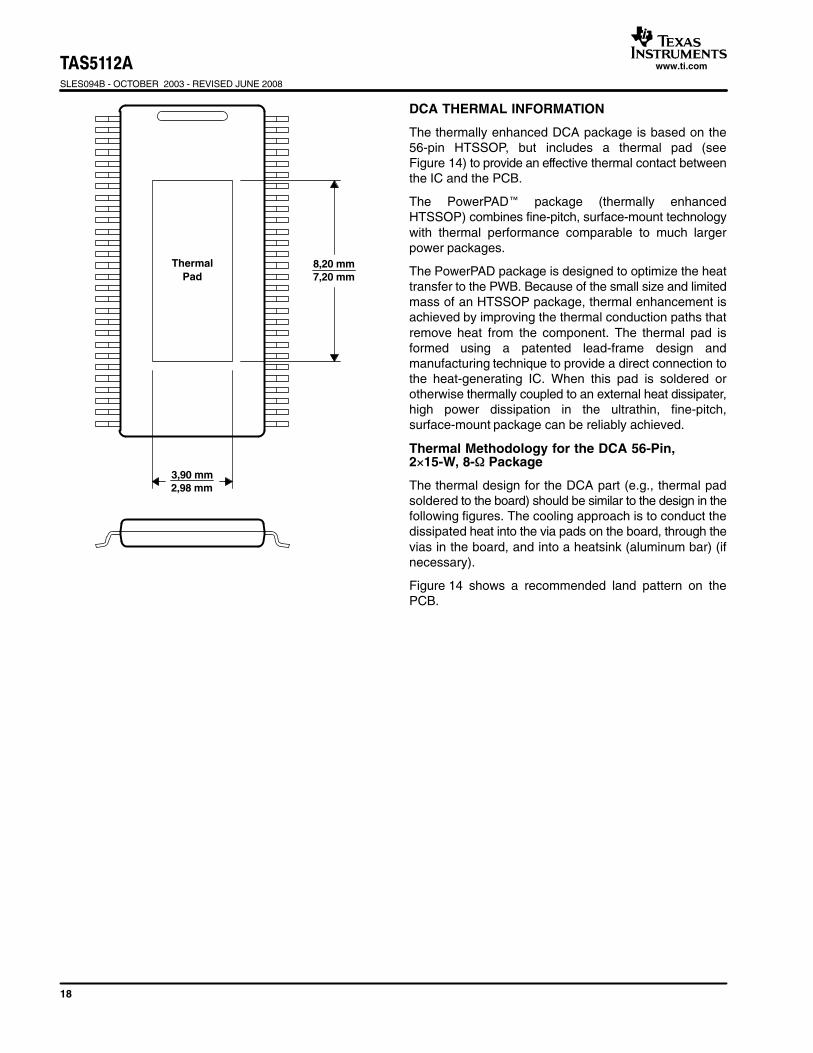
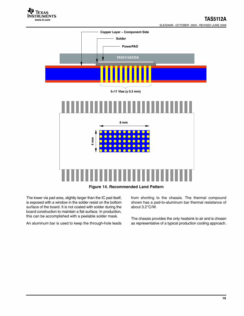
ThermalPad
8,20 mm7,20 mm
3,90 mm2,98 mm
DCA THERMAL INFORMATION
The thermally enhanced DCA package is based on the56-pin HTSSOP, but includes a thermal pad (seeFigure 14) to provide an effective thermal contact betweenthe IC and the PCB.
The PowerPAD™ package (thermally enhancedHTSSOP) combines fine-pitch, surface-mount technologywith thermal performance comparable to much largerpower packages.
The PowerPAD package is designed to optimize the heattransfer to the PWB. Because of the small size and limitedmass of an HTSSOP package, thermal enhancement isachieved by improving the thermal conduction paths thatremove heat from the component. The thermal pad isformed using a patented lead-frame design andmanufacturing technique to provide a direct connection tothe heat-generating IC. When this pad is soldered orotherwise thermally coupled to an external heat dissipater,high power dissipation in the ultrathin, fine-pitch,surface-mount package can be reliably achieved.
Thermal Methodology for the DCA 56-Pin,215-W, 8- Package
The thermal design for the DCA part (e.g., thermal padsoldered to the board) should be similar to the design in thefollowing figures. The cooling approach is to conduct thedissipated heat into the via pads on the board, through thevias in the board, and into a heatsink (aluminum bar) (ifnecessary).
Figure 14 shows a recommended land pattern on thePCB.
TAS5112ASLES094B - OCTOBER 2003 - REVISED JUNE 2008
www.ti.com
19
TAS5112ACDA
Copper Layer − Component Side
Solder
PowerPAD
4m
m
8 mm
511 Vias ( 0.3 mm)
Figure 14. Recommended Land Pattern
The lower via pad area, slightly larger than the IC pad itself,is exposed with a window in the solder resist on the bottomsurface of the board. It is not coated with solder during theboard construction to maintain a flat surface. In production,this can be accomplished with a peelable solder mask.
An aluminum bar is used to keep the through-hole leads
from shorting to the chassis. The thermal compoundshown has a pad-to-aluminum bar thermal resistance ofabout 3.2°C/W.
The chassis provides the only heatsink to air and is chosenas representative of a typical production cooling approach.
TAS5112ASLES094B - OCTOBER 2003 - REVISED JUNE 2008
www.ti.com
20
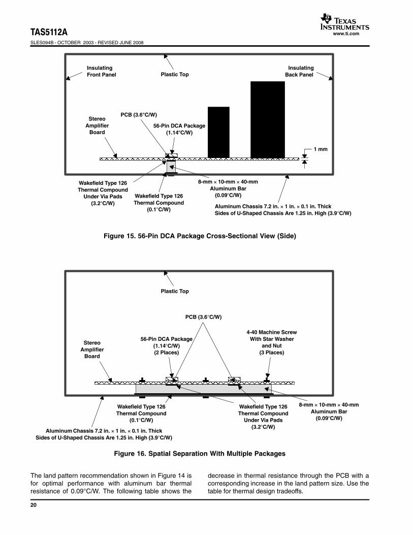
ÓÓÓÓÓÓÓÓÓÓÓÓÓÓÓÓÓÓÓÓÔÔÔÔÔÔ
Aluminum Chassis 7.2 in. 1 in. 0.1 in. ThickSides of U-Shaped Chassis Are 1.25 in. High (3.9°C/W)
56-Pin DCA Package(1.14C/W)
InsulatingBack Panel
InsulatingFront Panel
StereoAmplifier
Board
Wakefield Type 126Thermal Compound
Under Via Pads(3.2°C/W)
Wakefield Type 126Thermal Compound
(0.1°C/W)
8-mm 10-mm 40-mmAluminum Bar
(0.09°C/W)
1 mm
Plastic Top
PCB (3.6C/W)
Figure 15. 56-Pin DCA Package Cross-Sectional View (Side)
ÓÓÓÓÓÓÓÓÓÓÓÓÓÓÓÓÓÓÓÓÓÓÓÓÓÓÓÓÓÓÓÓÓÓÓÓÓÓÓÓ
ÔÔÔÖÖÖ ÔÔÖÖ
Aluminum Chassis 7.2 in. 1 in. 0.1 in. ThickSides of U-Shaped Chassis Are 1.25 in. High (3.9°C/W)
8-mm 10-mm 40-mmAluminum Bar
(0.09°C/W)
Plastic Top
Wakefield Type 126Thermal Compound
(0.1°C/W)
56-Pin DCA Package(1.14°C/W)(2 Places)
PCB (3.6°C/W)
Wakefield Type 126Thermal Compound
Under Via Pads(3.2°C/W)
4-40 Machine ScrewWith Star Washer
and Nut(3 Places)
StereoAmplifier
Board
Figure 16. Spatial Separation With Multiple Packages
The land pattern recommendation shown in Figure 14 isfor optimal performance with aluminum bar thermalresistance of 0.09°C/W. The following table shows the
decrease in thermal resistance through the PCB with acorresponding increase in the land pattern size. Use thetable for thermal design tradeoffs.
TAS5112ASLES094B - OCTOBER 2003 - REVISED JUNE 2008
www.ti.com
21
LAND PATTERNPCB THERMALRESISTANCE
7 × 13 vias (5 × 10 mm) 2.2°C/W
5 × 11 vias (4 × 8 mm) 3.6°C/W
ThermalPad
8,20 mm7,20 mm
3,90 mm2,98 mm
Figure 17. Thermal Pad Dimensions for DCAPackage
CLICK AND POP REDUCTION
TI modulators feature a pop and click reduction systemthat controls the timing when switching starts and stops.
Going from nonswitching to switching operation causes aspectral energy burst to occur within the audio bandwidth,which is heard in the speaker as an audible click, forinstance, after having asserted RESET LH during asystem start-up.
To make this system work properly, the following designrules must be followed when using the TAS5112A backend:
The relative timing between the PWM_AP/M_xsignals and their corresponding VALID_x signalshould not be skewed by inserting delays,because this increases the audible amplitudelevel of the click.
The output stage must start switching from afully discharged output filter capacitor. Becausethe output stage prior to operation is in thehigh-impedance state, this is done by having apassive pulldown resistor on each speakeroutput to GND (see System Configuration Usedfor Characterization).
Other things that can affect the audible click level:
The spectrum of the click seems to follow thespeaker impedance vs. frequency curve—thehigher the impedance, the higher the clickenergy.
Crossover filters used between woofer andtweeter in a speaker can have high impedancein the audio band, which should be avoided ifpossible.
Another way to look at it is that the speaker impulseresponse is a major contributor to how the click energy isshaped in the audio band and how audible the click will be.
The following mode transitions feature click and popreduction.
STATECLICK AND
POP REDUCED
Normal(1) → Mute Yes
Mute → Normal(1) Yes
Normal(1) →Error recovery(ERRCVY)
Yes
Error recovery → Normal(1) Yes
Normal(1) → Hard reset No
Hard reset → Normal(1) Yes(1) Normal = switching
TAS5112ASLES094B - OCTOBER 2003 - REVISED JUNE 2008
www.ti.com
22
REFERENCES
1. TAS5000 Digital Audio PWM Processor datamanual—TI (SLAS270)
2. True Digital Audio Amplifier TAS5001 Digital AudioPWM Processor data sheet—TI (SLES009)
3. True Digital Audio Amplifier TAS5010 Digital AudioPWM Processor data sheet—TI (SLAS328)
4. True Digital Audio Amplifier TAS5012 Digital AudioPWM Processor data sheet—TI (SLES006)
5. TAS5026 Six-Channel Digital Audio PWMProcessor data manual—TI (SLES041)
6. TAS5036A Six-Channel Digital Audio PWMProcessor data manual—TI (SLES061)
7. TAS3103 Digital Audio Processor With 3D Effectsdata manual—TI (SLES038)
8. Digital Audio Measurements application report—TI(SLAA114)
9. PowerPAD™ Thermally Enhanced Packagetechnical brief—TI (SLMA002)
10. System Design Considerations for True DigitalAudio Power Amplifiers application report—TI(SLAA117)
PACKAGE OPTION ADDENDUM
www.ti.com 10-Jun-2014
Addendum-Page 1
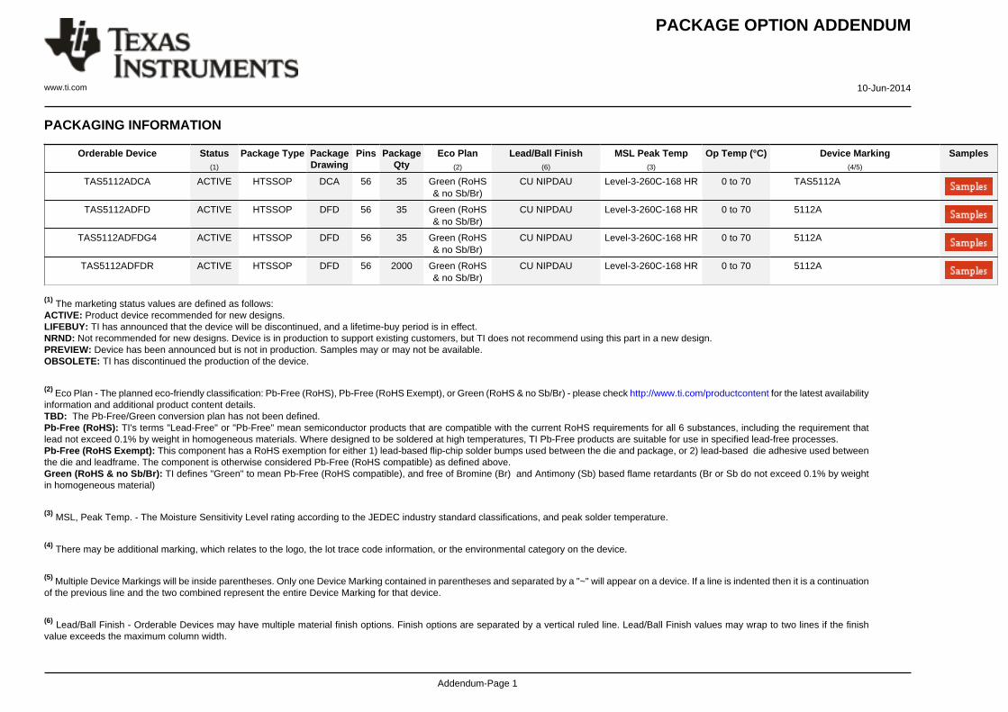
PACKAGING INFORMATION
Orderable Device Status(1)
Package Type PackageDrawing
Pins PackageQty
Eco Plan(2)
Lead/Ball Finish(6)
MSL Peak Temp(3)
Op Temp (°C) Device Marking(4/5)
Samples
TAS5112ADCA ACTIVE HTSSOP DCA 56 35 Green (RoHS& no Sb/Br)
CU NIPDAU Level-3-260C-168 HR 0 to 70 TAS5112A
TAS5112ADFD ACTIVE HTSSOP DFD 56 35 Green (RoHS& no Sb/Br)
CU NIPDAU Level-3-260C-168 HR 0 to 70 5112A
TAS5112ADFDG4 ACTIVE HTSSOP DFD 56 35 Green (RoHS& no Sb/Br)
CU NIPDAU Level-3-260C-168 HR 0 to 70 5112A
TAS5112ADFDR ACTIVE HTSSOP DFD 56 2000 Green (RoHS& no Sb/Br)
CU NIPDAU Level-3-260C-168 HR 0 to 70 5112A
(1) The marketing status values are defined as follows:ACTIVE: Product device recommended for new designs.LIFEBUY: TI has announced that the device will be discontinued, and a lifetime-buy period is in effect.NRND: Not recommended for new designs. Device is in production to support existing customers, but TI does not recommend using this part in a new design.PREVIEW: Device has been announced but is not in production. Samples may or may not be available.OBSOLETE: TI has discontinued the production of the device.
(2) Eco Plan - The planned eco-friendly classification: Pb-Free (RoHS), Pb-Free (RoHS Exempt), or Green (RoHS & no Sb/Br) - please check http://www.ti.com/productcontent for the latest availabilityinformation and additional product content details.TBD: The Pb-Free/Green conversion plan has not been defined.Pb-Free (RoHS): TI's terms "Lead-Free" or "Pb-Free" mean semiconductor products that are compatible with the current RoHS requirements for all 6 substances, including the requirement thatlead not exceed 0.1% by weight in homogeneous materials. Where designed to be soldered at high temperatures, TI Pb-Free products are suitable for use in specified lead-free processes.Pb-Free (RoHS Exempt): This component has a RoHS exemption for either 1) lead-based flip-chip solder bumps used between the die and package, or 2) lead-based die adhesive used betweenthe die and leadframe. The component is otherwise considered Pb-Free (RoHS compatible) as defined above.Green (RoHS & no Sb/Br): TI defines "Green" to mean Pb-Free (RoHS compatible), and free of Bromine (Br) and Antimony (Sb) based flame retardants (Br or Sb do not exceed 0.1% by weightin homogeneous material)
(3) MSL, Peak Temp. - The Moisture Sensitivity Level rating according to the JEDEC industry standard classifications, and peak solder temperature.
(4) There may be additional marking, which relates to the logo, the lot trace code information, or the environmental category on the device.
(5) Multiple Device Markings will be inside parentheses. Only one Device Marking contained in parentheses and separated by a "~" will appear on a device. If a line is indented then it is a continuationof the previous line and the two combined represent the entire Device Marking for that device.
(6) Lead/Ball Finish - Orderable Devices may have multiple material finish options. Finish options are separated by a vertical ruled line. Lead/Ball Finish values may wrap to two lines if the finishvalue exceeds the maximum column width.
PACKAGE OPTION ADDENDUM
www.ti.com 10-Jun-2014
Addendum-Page 2
Important Information and Disclaimer:The information provided on this page represents TI's knowledge and belief as of the date that it is provided. TI bases its knowledge and belief on informationprovided by third parties, and makes no representation or warranty as to the accuracy of such information. Efforts are underway to better integrate information from third parties. TI has taken andcontinues to take reasonable steps to provide representative and accurate information but may not have conducted destructive testing or chemical analysis on incoming materials and chemicals.TI and TI suppliers consider certain information to be proprietary, and thus CAS numbers and other limited information may not be available for release.
In no event shall TI's liability arising out of such information exceed the total purchase price of the TI part(s) at issue in this document sold by TI to Customer on an annual basis.
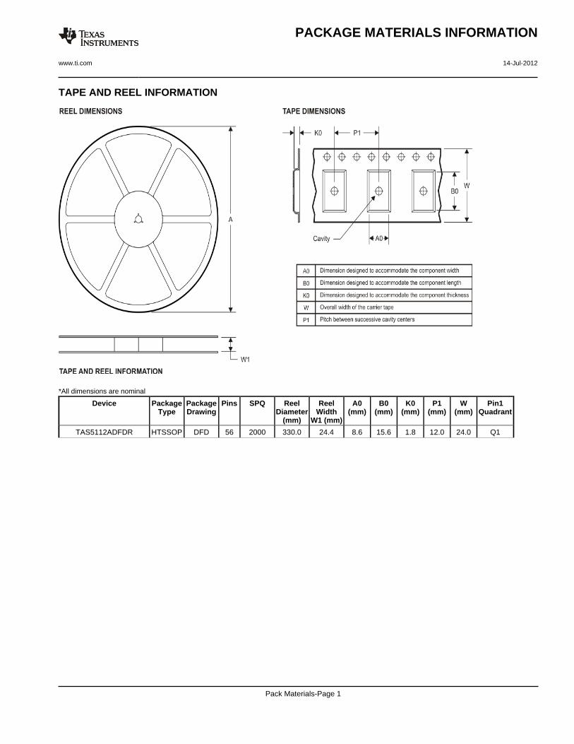
TAPE AND REEL INFORMATION
*All dimensions are nominal
Device PackageType
PackageDrawing
Pins SPQ ReelDiameter
(mm)
ReelWidth
W1 (mm)
A0(mm)
B0(mm)
K0(mm)
P1(mm)
W(mm)
Pin1Quadrant
TAS5112ADFDR HTSSOP DFD 56 2000 330.0 24.4 8.6 15.6 1.8 12.0 24.0 Q1
PACKAGE MATERIALS INFORMATION
www.ti.com 14-Jul-2012
Pack Materials-Page 1
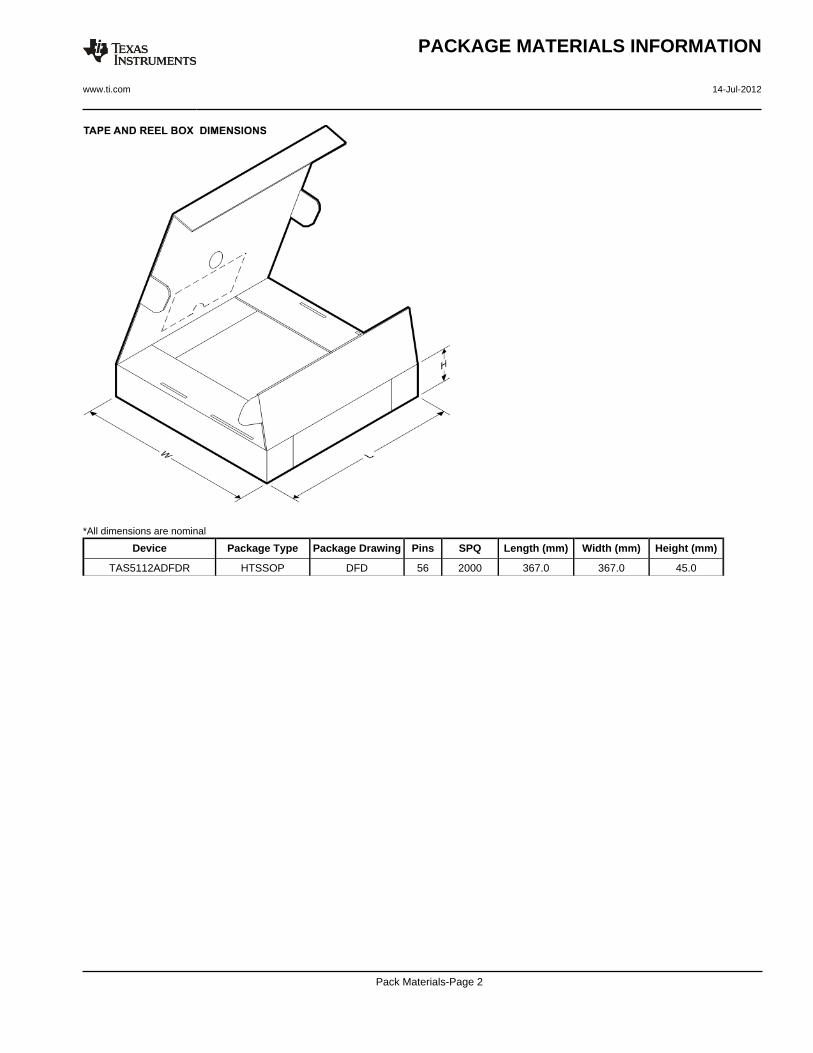
*All dimensions are nominal
Device Package Type Package Drawing Pins SPQ Length (mm) Width (mm) Height (mm)
TAS5112ADFDR HTSSOP DFD 56 2000 367.0 367.0 45.0
PACKAGE MATERIALS INFORMATION
www.ti.com 14-Jul-2012
Pack Materials-Page 2
IMPORTANT NOTICETexas Instruments Incorporated and its subsidiaries (TI) reserve the right to make corrections, enhancements, improvements and otherchanges to its semiconductor products and services per JESD46, latest issue, and to discontinue any product or service per JESD48, latestissue. Buyers should obtain the latest relevant information before placing orders and should verify that such information is current andcomplete. All semiconductor products (also referred to herein as “components”) are sold subject to TI’s terms and conditions of salesupplied at the time of order acknowledgment.TI warrants performance of its components to the specifications applicable at the time of sale, in accordance with the warranty in TI’s termsand conditions of sale of semiconductor products. Testing and other quality control techniques are used to the extent TI deems necessaryto support this warranty. Except where mandated by applicable law, testing of all parameters of each component is not necessarilyperformed.TI assumes no liability for applications assistance or the design of Buyers’ products. Buyers are responsible for their products andapplications using TI components. To minimize the risks associated with Buyers’ products and applications, Buyers should provideadequate design and operating safeguards.TI does not warrant or represent that any license, either express or implied, is granted under any patent right, copyright, mask work right, orother intellectual property right relating to any combination, machine, or process in which TI components or services are used. Informationpublished by TI regarding third-party products or services does not constitute a license to use such products or services or a warranty orendorsement thereof. Use of such information may require a license from a third party under the patents or other intellectual property of thethird party, or a license from TI under the patents or other intellectual property of TI.Reproduction of significant portions of TI information in TI data books or data sheets is permissible only if reproduction is without alterationand is accompanied by all associated warranties, conditions, limitations, and notices. TI is not responsible or liable for such altereddocumentation. Information of third parties may be subject to additional restrictions.Resale of TI components or services with statements different from or beyond the parameters stated by TI for that component or servicevoids all express and any implied warranties for the associated TI component or service and is an unfair and deceptive business practice.TI is not responsible or liable for any such statements.Buyer acknowledges and agrees that it is solely responsible for compliance with all legal, regulatory and safety-related requirementsconcerning its products, and any use of TI components in its applications, notwithstanding any applications-related information or supportthat may be provided by TI. Buyer represents and agrees that it has all the necessary expertise to create and implement safeguards whichanticipate dangerous consequences of failures, monitor failures and their consequences, lessen the likelihood of failures that might causeharm and take appropriate remedial actions. Buyer will fully indemnify TI and its representatives against any damages arising out of the useof any TI components in safety-critical applications.In some cases, TI components may be promoted specifically to facilitate safety-related applications. With such components, TI’s goal is tohelp enable customers to design and create their own end-product solutions that meet applicable functional safety standards andrequirements. Nonetheless, such components are subject to these terms.No TI components are authorized for use in FDA Class III (or similar life-critical medical equipment) unless authorized officers of the partieshave executed a special agreement specifically governing such use.Only those TI components which TI has specifically designated as military grade or “enhanced plastic” are designed and intended for use inmilitary/aerospace applications or environments. Buyer acknowledges and agrees that any military or aerospace use of TI componentswhich have not been so designated is solely at the Buyer's risk, and that Buyer is solely responsible for compliance with all legal andregulatory requirements in connection with such use.TI has specifically designated certain components as meeting ISO/TS16949 requirements, mainly for automotive use. In any case of use ofnon-designated products, TI will not be responsible for any failure to meet ISO/TS16949.Products ApplicationsAudio www.ti.com/audio Automotive and Transportation www.ti.com/automotiveAmplifiers amplifier.ti.com Communications and Telecom www.ti.com/communicationsData Converters dataconverter.ti.com Computers and Peripherals www.ti.com/computersDLP® Products www.dlp.com Consumer Electronics www.ti.com/consumer-appsDSP dsp.ti.com Energy and Lighting www.ti.com/energyClocks and Timers www.ti.com/clocks Industrial www.ti.com/industrialInterface interface.ti.com Medical www.ti.com/medicalLogic logic.ti.com Security www.ti.com/securityPower Mgmt power.ti.com Space, Avionics and Defense www.ti.com/space-avionics-defenseMicrocontrollers microcontroller.ti.com Video and Imaging www.ti.com/videoRFID www.ti-rfid.comOMAP Applications Processors www.ti.com/omap TI E2E Community e2e.ti.comWireless Connectivity www.ti.com/wirelessconnectivity
Mailing Address: Texas Instruments, Post Office Box 655303, Dallas, Texas 75265Copyright © 2014, Texas Instruments Incorporated