
EECS150 - Digital Design Lecture 18 - Circuit Timing (2)cs150/sp10/Lecture/lec18-timing2.pdf ·...
15
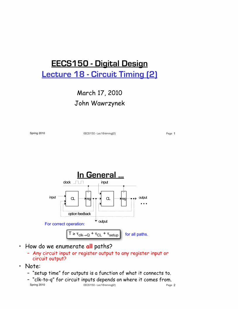
Spring 2010 EECS150 - Lec18-timing(2) Page EECS150 - Digital Design Lecture 18 - Circuit Timing (2) March 17, 2010 John Wawrzynek 1 Spring 2010 EECS150 - Lec18-timing(2) Page In General ... T ≥ τ clk→Q + τ CL + τ setup 2 For correct operation: for all paths. • How do we enumerate all paths? – Any circuit input or register output to any register input or circuit output? • Note: – “setup time” for outputs is a function of what it connects to. – “clk-to-q” for circuit inputs depends on where it comes from.
Transcript of EECS150 - Digital Design Lecture 18 - Circuit Timing (2)cs150/sp10/Lecture/lec18-timing2.pdf ·...
Spring 2010 EECS150 - Lec18-timing(2) Page
EECS150 - Digital DesignLecture 18 - Circuit Timing (2)
March 17, 2010John Wawrzynek
1
Spring 2010 EECS150 - Lec18-timing(2) Page
In General ...
T ≥ τclk→Q + τCL + τsetup
2
For correct operation:
for all paths.
• How do we enumerate all paths?– Any circuit input or register output to any register input or
circuit output?• Note:
– “setup time” for outputs is a function of what it connects to.– “clk-to-q” for circuit inputs depends on where it comes from.
Spring 2010 EECS150 - Lec18-timing(2) Page
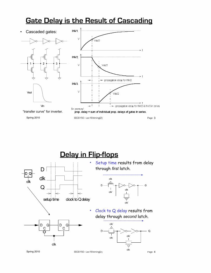
Gate Delay is the Result of Cascading• Cascaded gates:
“transfer curve” for inverter.
3
Spring 2010 EECS150 - Lec18-timing(2) Page
Delay in Flip-flops• Setup time results from delay
through first latch.
• Clock to Q delay results from delay through second latch.
clk
clk’
clk
clk’
clk
clk’
clk
clk’
4
Spring 2010 EECS150 - Lec18-timing(2) Page
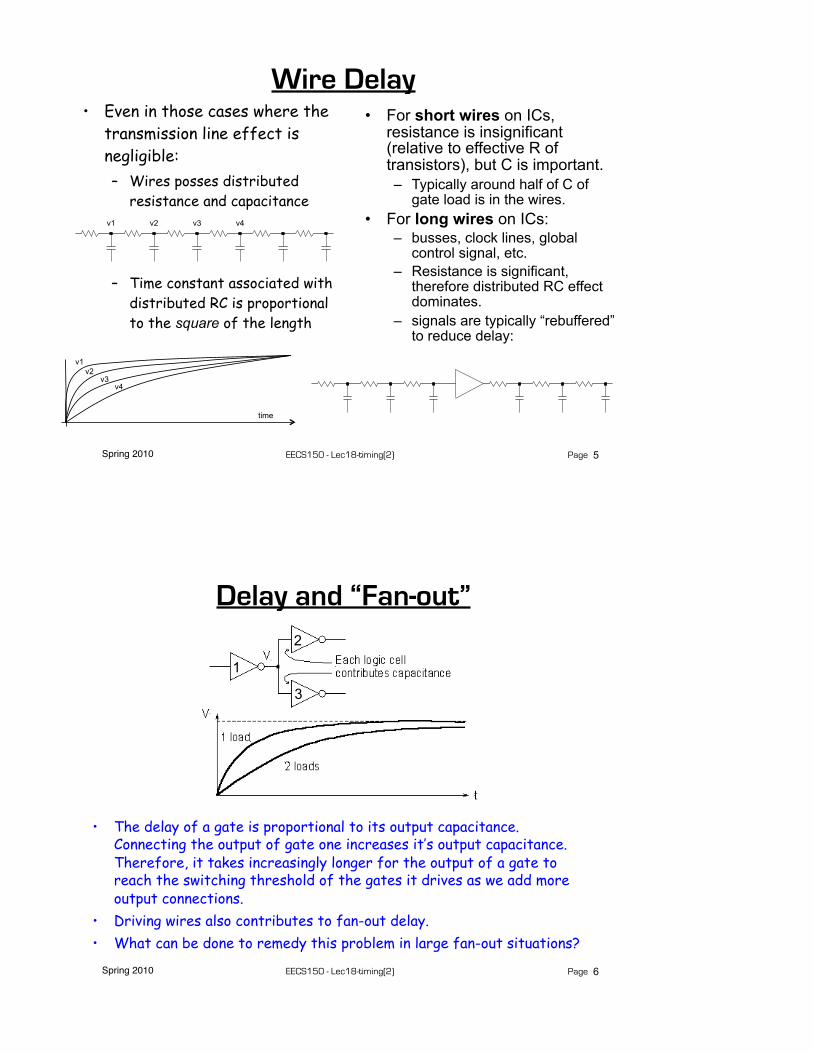
Wire Delay• Even in those cases where the
transmission line effect is negligible:– Wires posses distributed
resistance and capacitance
– Time constant associated with distributed RC is proportional to the square of the length
• For short wires on ICs, resistance is insignificant (relative to effective R of transistors), but C is important.– Typically around half of C of
gate load is in the wires.• For long wires on ICs:
– busses, clock lines, global control signal, etc.
– Resistance is significant, therefore distributed RC effect dominates.
– signals are typically “rebuffered” to reduce delay:
v1 v2 v3 v4
5
v1
v4v3
v2
time
Spring 2010 EECS150 - Lec18-timing(2) Page
Delay and “Fan-out”
• The delay of a gate is proportional to its output capacitance. Connecting the output of gate one increases it’s output capacitance. Therefore, it takes increasingly longer for the output of a gate to reach the switching threshold of the gates it drives as we add more output connections.
• Driving wires also contributes to fan-out delay.• What can be done to remedy this problem in large fan-out situations?
1
3
2
6
Spring 2010 EECS150 - Lec18-timing(2) Page
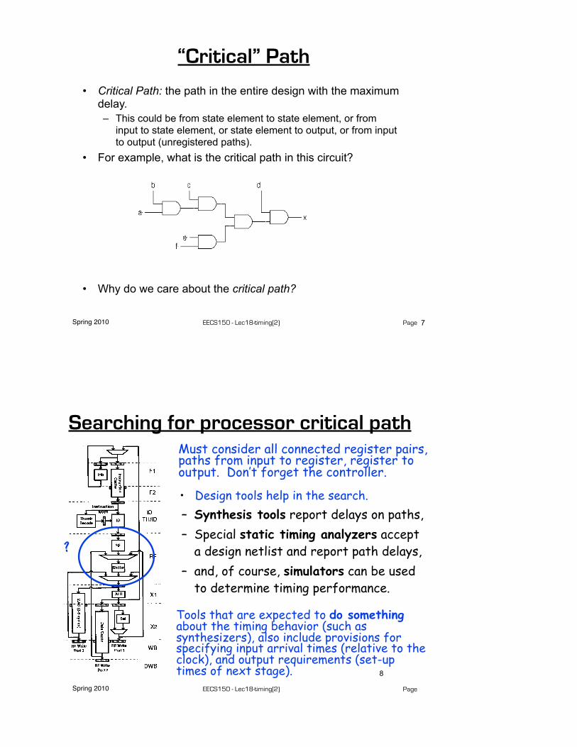
“Critical” Path
• Critical Path: the path in the entire design with the maximum delay.– This could be from state element to state element, or from
input to state element, or state element to output, or from input to output (unregistered paths).
• For example, what is the critical path in this circuit?
• Why do we care about the critical path?
7
Spring 2010 EECS150 - Lec18-timing(2) Page
Searching for processor critical path1600 IEEE JOURNAL OF SOLID-STATE CIRCUITS, VOL. 36, NO. 11, NOVEMBER 2001
Fig. 1. Process SEM cross section.
The process was raised from [1] to limit standby power.
Circuit design and architectural pipelining ensure low voltage
performance and functionality. To further limit standby current
in handheld ASSPs, a longer poly target takes advantage of the
versus dependence and source-to-body bias is used
to electrically limit transistor in standby mode. All core
nMOS and pMOS transistors utilize separate source and bulk
connections to support this. The process includes cobalt disili-
cide gates and diffusions. Low source and drain capacitance, as
well as 3-nm gate-oxide thickness, allow high performance and
low-voltage operation.
III. ARCHITECTURE
The microprocessor contains 32-kB instruction and data
caches as well as an eight-entry coalescing writeback buffer.
The instruction and data cache fill buffers have two and four
entries, respectively. The data cache supports hit-under-miss
operation and lines may be locked to allow SRAM-like oper-
ation. Thirty-two-entry fully associative translation lookaside
buffers (TLBs) that support multiple page sizes are provided
for both caches. TLB entries may also be locked. A 128-entry
branch target buffer improves branch performance a pipeline
deeper than earlier high-performance ARM designs [2], [3].
A. Pipeline Organization
To obtain high performance, the microprocessor core utilizes
a simple scalar pipeline and a high-frequency clock. In addition
to avoiding the potential power waste of a superscalar approach,
functional design and validation complexity is decreased at the
expense of circuit design effort. To avoid circuit design issues,
the pipeline partitioning balances the workload and ensures that
no one pipeline stage is tight. The main integer pipeline is seven
stages, memory operations follow an eight-stage pipeline, and
when operating in thumb mode an extra pipe stage is inserted
after the last fetch stage to convert thumb instructions into ARM
instructions. Since thumb mode instructions [11] are 16 b, two
instructions are fetched in parallel while executing thumb in-
structions. A simplified diagram of the processor pipeline is
Fig. 2. Microprocessor pipeline organization.
shown in Fig. 2, where the state boundaries are indicated by
gray. Features that allow the microarchitecture to achieve high
speed are as follows.
The shifter and ALU reside in separate stages. The ARM in-
struction set allows a shift followed by an ALU operation in a
single instruction. Previous implementations limited frequency
by having the shift and ALU in a single stage. Splitting this op-
eration reduces the critical ALU bypass path by approximately
1/3. The extra pipeline hazard introduced when an instruction is
immediately followed by one requiring that the result be shifted
is infrequent.
Decoupled Instruction Fetch.A two-instruction deep queue is
implemented between the second fetch and instruction decode
pipe stages. This allows stalls generated later in the pipe to be
deferred by one or more cycles in the earlier pipe stages, thereby
allowing instruction fetches to proceed when the pipe is stalled,
and also relieves stall speed paths in the instruction fetch and
branch prediction units.
Deferred register dependency stalls. While register depen-
dencies are checked in the RF stage, stalls due to these hazards
are deferred until the X1 stage. All the necessary operands are
then captured from result-forwarding busses as the results are
returned to the register file.
One of the major goals of the design was to minimize the en-
ergy consumed to complete a given task. Conventional wisdom
has been that shorter pipelines are more efficient due to re-
Must consider all connected register pairs, paths from input to register, register to output. Don’t forget the controller.
?
8
• Design tools help in the search. – Synthesis tools report delays on paths, – Special static timing analyzers accept
a design netlist and report path delays, – and, of course, simulators can be used
to determine timing performance.
Tools that are expected to do something about the timing behavior (such as synthesizers), also include provisions for specifying input arrival times (relative to the clock), and output requirements (set-up times of next stage).
Spring 2010 EECS150 - Lec18-timing(2) Page
Real Stuff: Timing Analysis
From “The circuit and physical design of the POWER4 microprocessor”, IBM J Res and Dev, 46:1, Jan 2002, J.D. Warnock et al.
netlist. Of these, 121 713 were top-level chip global nets,and 21 711 were processor-core-level global nets. Againstthis model 3.5 million setup checks were performed in latemode at points where clock signals met data signals inlatches or dynamic circuits. The total number of timingchecks of all types performed in each chip run was9.8 million. Depending on the configuration of the timingrun and the mix of actual versus estimated design data,the amount of real memory required was in the rangeof 12 GB to 14 GB, with run times of about 5 to 6 hoursto the start of timing-report generation on an RS/6000*Model S80 configured with 64 GB of real memory.Approximately half of this time was taken up by readingin the netlist, timing rules, and extracted RC networks, as
well as building and initializing the internal data structuresfor the timing model. The actual static timing analysistypically took 2.5–3 hours. Generation of the entirecomplement of reports and analysis required an additional5 to 6 hours to complete. A total of 1.9 GB of timingreports and analysis were generated from each chip timingrun. This data was broken down, analyzed, and organizedby processor core and GPS, individual unit, and, in thecase of timing contracts, by unit and macro. This was onecomponent of the 24-hour-turnaround time achieved forthe chip-integration design cycle. Figure 26 shows theresults of iterating this process: A histogram of the finalnominal path delays obtained from static timing for thePOWER4 processor.
The POWER4 design includes LBIST and ABIST(Logic/Array Built-In Self-Test) capability to enable full-frequency ac testing of the logic and arrays. Such testingon pre-final POWER4 chips revealed that several circuitmacros ran slower than predicted from static timing. Thespeed of the critical paths in these macros was increasedin the final design. Typical fast ac LBIST laboratory testresults measured on POWER4 after these paths wereimproved are shown in Figure 27.
SummaryThe 174-million-transistor !1.3-GHz POWER4 chip,containing two microprocessor cores and an on-chipmemory subsystem, is a large, complex, high-frequencychip designed by a multi-site design team. Theperformance and schedule goals set at the beginning ofthe project were met successfully. This paper describesthe circuit and physical design of POWER4, emphasizingaspects that were important to the project’s success in theareas of design methodology, clock distribution, circuits,power, integration, and timing.
Figure 25
POWER4 timing flow. This process was iterated daily during the physical design phase to close timing.
VIM
Timer files ReportsAsserts
Spice
Spice
GL/1
Reports
< 12 hr
< 12 hr
< 12 hr
< 48 hr
< 24 hr
Non-uplift timing
Noiseimpacton timing
Upliftanalysis
Capacitanceadjust
Chipbench /EinsTimer
Chipbench /EinsTimer
Extraction
Core or chipwiring
Analysis/update(wires, buffers)
Notes:• Executed 2–3 months prior to tape-out• Fully extracted data from routed designs • Hierarchical extraction• Custom logic handled separately • Dracula • Harmony• Extraction done for • Early • Late
Extracted units (flat or hierarchical)Incrementally extracted RLMsCustom NDRsVIMs
Figure 26
Histogram of the POWER4 processor path delays.
!40 !20 0 20 40 60 80 100 120 140 160 180 200 220 240 260 280Timing slack (ps)
Lat
e-m
ode
timin
g ch
ecks
(th
ousa
nds)
0
50
100
150
200
IBM J. RES. & DEV. VOL. 46 NO. 1 JANUARY 2002 J. D. WARNOCK ET AL.
47
Most paths have hundreds of picoseconds to spare.The critical path
9
Spring 2010 EECS150 - Lec18-timing(2) Page
Clock Skew
• Unequal delay in distribution of the clock signal to various parts of a circuit:– if not accounted for, can lead to erroneous behavior.– Comes about because:
• clock wires have delay,• circuit is designed with a different number of clock buffers from
the clock source to the various clock loads, or• buffers have unequal delay.
– All synchronous circuits experience some clock skew:• more of an issue for high-performance designs operating with very
little extra time per clock cycle.
clock skew, delay in distribution
10
Spring 2010 EECS150 - Lec18-timing(2) Page
Clock Skew (cont.)
• If clock period T = TCL+Tsetup+Tclk→Q, circuit will fail.
• Therefore:1. Control clock skew a) Careful clock distribution. Equalize path delay from clock source to
all clock loads by controlling wires delay and buffer delay. b) don’t “gate” clocks in a non-uniform way.2. T ≥ TCL+Tsetup+Tclk→Q + worst case skew.
• Most modern large high-performance chips (microprocessors) control end to end clock skew to a small fraction of the clock period.
clock skew, delay in distributionCL
CLKCLK’
CLK
CLK’
11
Spring 2010 EECS150 - Lec18-timing(2) Page
Clock Skew (cont.)
• Note reversed buffer.• In this case, clock skew actually provides extra time (adds to
the effective clock period).• This effect has been used to help run circuits as higher
clock rates. Risky business!
CL
CLKCLK’
clock skew, delay in distribution
CLK
CLK’
12
Spring 2010 EECS150 - Lec18-timing(2) Page
1600 IEEE JOURNAL OF SOLID-STATE CIRCUITS, VOL. 36, NO. 11, NOVEMBER 2001
Fig. 1. Process SEM cross section.
The process was raised from [1] to limit standby power.
Circuit design and architectural pipelining ensure low voltage
performance and functionality. To further limit standby current
in handheld ASSPs, a longer poly target takes advantage of the
versus dependence and source-to-body bias is used
to electrically limit transistor in standby mode. All core
nMOS and pMOS transistors utilize separate source and bulk
connections to support this. The process includes cobalt disili-
cide gates and diffusions. Low source and drain capacitance, as
well as 3-nm gate-oxide thickness, allow high performance and
low-voltage operation.
III. ARCHITECTURE
The microprocessor contains 32-kB instruction and data
caches as well as an eight-entry coalescing writeback buffer.
The instruction and data cache fill buffers have two and four
entries, respectively. The data cache supports hit-under-miss
operation and lines may be locked to allow SRAM-like oper-
ation. Thirty-two-entry fully associative translation lookaside
buffers (TLBs) that support multiple page sizes are provided
for both caches. TLB entries may also be locked. A 128-entry
branch target buffer improves branch performance a pipeline
deeper than earlier high-performance ARM designs [2], [3].
A. Pipeline Organization
To obtain high performance, the microprocessor core utilizes
a simple scalar pipeline and a high-frequency clock. In addition
to avoiding the potential power waste of a superscalar approach,
functional design and validation complexity is decreased at the
expense of circuit design effort. To avoid circuit design issues,
the pipeline partitioning balances the workload and ensures that
no one pipeline stage is tight. The main integer pipeline is seven
stages, memory operations follow an eight-stage pipeline, and
when operating in thumb mode an extra pipe stage is inserted
after the last fetch stage to convert thumb instructions into ARM
instructions. Since thumb mode instructions [11] are 16 b, two
instructions are fetched in parallel while executing thumb in-
structions. A simplified diagram of the processor pipeline is
Fig. 2. Microprocessor pipeline organization.
shown in Fig. 2, where the state boundaries are indicated by
gray. Features that allow the microarchitecture to achieve high
speed are as follows.
The shifter and ALU reside in separate stages. The ARM in-
struction set allows a shift followed by an ALU operation in a
single instruction. Previous implementations limited frequency
by having the shift and ALU in a single stage. Splitting this op-
eration reduces the critical ALU bypass path by approximately
1/3. The extra pipeline hazard introduced when an instruction is
immediately followed by one requiring that the result be shifted
is infrequent.
Decoupled Instruction Fetch.A two-instruction deep queue is
implemented between the second fetch and instruction decode
pipe stages. This allows stalls generated later in the pipe to be
deferred by one or more cycles in the earlier pipe stages, thereby
allowing instruction fetches to proceed when the pipe is stalled,
and also relieves stall speed paths in the instruction fetch and
branch prediction units.
Deferred register dependency stalls. While register depen-
dencies are checked in the RF stage, stalls due to these hazards
are deferred until the X1 stage. All the necessary operands are
then captured from result-forwarding busses as the results are
returned to the register file.
One of the major goals of the design was to minimize the en-
ergy consumed to complete a given task. Conventional wisdom
has been that shorter pipelines are more efficient due to re-
Real Stuff: Floorplanning Intel XScale 80200
13
Spring 2010 EECS150 - Lec18-timing(2) Page
the total wire delay is similar to the total buffer delay. Apatented tuning algorithm [16] was required to tune themore than 2000 tunable transmission lines in these sectortrees to achieve low skew, visualized as the flatness of thegrid in the 3D visualizations. Figure 8 visualizes four ofthe 64 sector trees containing about 125 tuned wiresdriving 1/16th of the clock grid. While symmetric H-treeswere desired, silicon and wiring blockages often forcedmore complex tree structures, as shown. Figure 8 alsoshows how the longer wires are split into multiple-fingeredtransmission lines interspersed with Vdd and ground shields(not shown) for better inductance control [17, 18]. Thisstrategy of tunable trees driving a single grid results in lowskew among any of the 15 200 clock pins on the chip,regardless of proximity.
From the global clock grid, a hierarchy of short clockroutes completed the connection from the grid down tothe individual local clock buffer inputs in the macros.These clock routing segments included wires at the macrolevel from the macro clock pins to the input of the localclock buffer, wires at the unit level from the macro clockpins to the unit clock pins, and wires at the chip levelfrom the unit clock pins to the clock grid.
Design methodology and resultsThis clock-distribution design method allows a highlyproductive combination of top-down and bottom-up designperspectives, proceeding in parallel and meeting at thesingle clock grid, which is designed very early. The treesdriving the grid are designed top-down, with the maximumwire widths contracted for them. Once the contract for thegrid had been determined, designers were insulated fromchanges to the grid, allowing necessary adjustments to thegrid to be made for minimizing clock skew even at a verylate stage in the design process. The macro, unit, and chipclock wiring proceeded bottom-up, with point tools ateach hierarchical level (e.g., macro, unit, core, and chip)using contracted wiring to form each segment of the totalclock wiring. At the macro level, short clock routesconnected the macro clock pins to the local clock buffers.These wires were kept very short, and duplication ofexisting higher-level clock routes was avoided by allowingthe use of multiple clock pins. At the unit level, clockrouting was handled by a special tool, which connected themacro pins to unit-level pins, placed as needed in pre-assigned wiring tracks. The final connection to the fixed
Figure 6
Schematic diagram of global clock generation and distribution.
PLL
Bypass
Referenceclock in
Referenceclock out
Clock distributionClock out
Figure 7
3D visualization of the entire global clock network. The x and y coordinates are chip x, y, while the z axis is used to represent delay, so the lowest point corresponds to the beginning of the clock distribution and the final clock grid is at the top. Widths are proportional to tuned wire width, and the three levels of buffers appear as vertical lines.
Del
ay
Grid
Tunedsectortrees
Sectorbuffers
Buffer level 2
Buffer level 1
y
x
Figure 8
Visualization of four of the 64 sector trees driving the clock grid, using the same representation as Figure 7. The complex sector trees and multiple-fingered transmission lines used for inductance control are visible at this scale.
Del
ay Multiple-fingeredtransmissionline
yx
J. D. WARNOCK ET AL. IBM J. RES. & DEV. VOL. 46 NO. 1 JANUARY 2002
32
Clock Tree Delays,
IBM “Power” CPU
Dela
y
14
Spring 2010 EECS150 - Lec18-timing(2) Page
the total wire delay is similar to the total buffer delay. Apatented tuning algorithm [16] was required to tune themore than 2000 tunable transmission lines in these sectortrees to achieve low skew, visualized as the flatness of thegrid in the 3D visualizations. Figure 8 visualizes four ofthe 64 sector trees containing about 125 tuned wiresdriving 1/16th of the clock grid. While symmetric H-treeswere desired, silicon and wiring blockages often forcedmore complex tree structures, as shown. Figure 8 alsoshows how the longer wires are split into multiple-fingeredtransmission lines interspersed with Vdd and ground shields(not shown) for better inductance control [17, 18]. Thisstrategy of tunable trees driving a single grid results in lowskew among any of the 15 200 clock pins on the chip,regardless of proximity.
From the global clock grid, a hierarchy of short clockroutes completed the connection from the grid down tothe individual local clock buffer inputs in the macros.These clock routing segments included wires at the macrolevel from the macro clock pins to the input of the localclock buffer, wires at the unit level from the macro clockpins to the unit clock pins, and wires at the chip levelfrom the unit clock pins to the clock grid.
Design methodology and resultsThis clock-distribution design method allows a highlyproductive combination of top-down and bottom-up designperspectives, proceeding in parallel and meeting at thesingle clock grid, which is designed very early. The treesdriving the grid are designed top-down, with the maximumwire widths contracted for them. Once the contract for thegrid had been determined, designers were insulated fromchanges to the grid, allowing necessary adjustments to thegrid to be made for minimizing clock skew even at a verylate stage in the design process. The macro, unit, and chipclock wiring proceeded bottom-up, with point tools ateach hierarchical level (e.g., macro, unit, core, and chip)using contracted wiring to form each segment of the totalclock wiring. At the macro level, short clock routesconnected the macro clock pins to the local clock buffers.These wires were kept very short, and duplication ofexisting higher-level clock routes was avoided by allowingthe use of multiple clock pins. At the unit level, clockrouting was handled by a special tool, which connected themacro pins to unit-level pins, placed as needed in pre-assigned wiring tracks. The final connection to the fixed
Figure 6
Schematic diagram of global clock generation and distribution.
PLL
Bypass
Referenceclock in
Referenceclock out
Clock distributionClock out
Figure 7
3D visualization of the entire global clock network. The x and y coordinates are chip x, y, while the z axis is used to represent delay, so the lowest point corresponds to the beginning of the clock distribution and the final clock grid is at the top. Widths are proportional to tuned wire width, and the three levels of buffers appear as vertical lines.
Del
ay
Grid
Tunedsectortrees
Sectorbuffers
Buffer level 2
Buffer level 1
y
x
Figure 8
Visualization of four of the 64 sector trees driving the clock grid, using the same representation as Figure 7. The complex sector trees and multiple-fingered transmission lines used for inductance control are visible at this scale.
Del
ay Multiple-fingeredtransmissionline
yx
J. D. WARNOCK ET AL. IBM J. RES. & DEV. VOL. 46 NO. 1 JANUARY 2002
32
Clock Tree Delays, IBM Power
clock grid was completed with a tool run at the chip level,connecting unit-level pins to the grid. At this point, theclock tuning and the bottom-up clock routing process stillhave a great deal of flexibility to respond rapidly to evenlate changes. Repeated practice routing and tuning wereperformed by a small, focused global clock team as theclock pins and buffer placements evolved to guaranteefeasibility and speed the design process.
Measurements of jitter and skew can be carried outusing the I/Os on the chip. In addition, approximately 100top-metal probe pads were included for direct probingof the global clock grid and buffers. Results on actualPOWER4 microprocessor chips show long-distanceskews ranging from 20 ps to 40 ps (cf. Figure 9). This isimproved from early test-chip hardware, which showedas much as 70 ps skew from across-chip channel-lengthvariations [19]. Detailed waveforms at the input andoutput of each global clock buffer were also measuredand compared with simulation to verify the specializedmodeling used to design the clock grid. Good agreementwas found. Thus, we have achieved a “correct-by-design”clock-distribution methodology. It is based on our designexperience and measurements from a series of increasinglyfast, complex server microprocessors. This method resultsin a high-quality global clock without having to usefeedback or adjustment circuitry to control skews.
Circuit designThe cycle-time target for the processor was set early in theproject and played a fundamental role in defining thepipeline structure and shaping all aspects of the circuitdesign as implementation proceeded. Early on, criticaltiming paths through the processor were simulated indetail in order to verify the feasibility of the designpoint and to help structure the pipeline for maximumperformance. Based on this early work, the goal for therest of the circuit design was to match the performance setduring these early studies, with custom design techniquesfor most of the dataflow macros and logic synthesis formost of the control logic—an approach similar to thatused previously [20]. Special circuit-analysis and modelingtechniques were used throughout the design in order toallow full exploitation of all of the benefits of the IBMadvanced SOI technology.
The sheer size of the chip, its complexity, and thenumber of transistors placed some important constraintson the design which could not be ignored in the push tomeet the aggressive cycle-time target on schedule. Theseconstraints led to the adoption of a primarily static-circuitdesign strategy, with dynamic circuits used only sparinglyin SRAMs and other critical regions of the processor core.Power dissipation was a significant concern, and it was akey factor in the decision to adopt a predominantly static-circuit design approach. In addition, the SOI technology,
including uncertainties associated with the modelingof the floating-body effect [21–23] and its impact onnoise immunity [22, 24 –27] and overall chip decouplingcapacitance requirements [26], was another factor behindthe choice of a primarily static design style. Finally, thesize and logical complexity of the chip posed risks tomeeting the schedule; choosing a simple, robust circuitstyle helped to minimize overall risk to the projectschedule with most efficient use of CAD tool and designresources. The size and complexity of the chip alsorequired rigorous testability guidelines, requiring almostall cycle boundary latches to be LSSD-compatible formaximum dc and ac test coverage.
Another important circuit design constraint was thelimit placed on signal slew rates. A global slew rate limitequal to one third of the cycle time was set and enforcedfor all signals (local and global) across the whole chip.The goal was to ensure a robust design, minimizingthe effects of coupled noise on chip timing and alsominimizing the effects of wiring-process variability onoverall path delay. Nets with poor slew also were foundto be more sensitive to device process variations andmodeling uncertainties, even where long wires and RCdelays were not significant factors. The general philosophywas that chip cycle-time goals also had to include theslew-limit targets; it was understood from the beginningthat the real hardware would function at the desiredcycle time only if the slew-limit targets were also met.
The following sections describe how these designconstraints were met without sacrificing cycle time. Thelatch design is described first, including a description ofthe local clocking scheme and clock controls. Then thecircuit design styles are discussed, including a description
Figure 9
Global clock waveforms showing 20 ps of measured skew.
1.5
1.0
0.5
0.0
0 500 1000 1500 2000 2500
20 ps skew
Vol
ts (
V)
Time (ps)
IBM J. RES. & DEV. VOL. 46 NO. 1 JANUARY 2002 J. D. WARNOCK ET AL.
33
15
Timing in Xilinx Designs
From earlier lecture: Virtex-5 slice
194 www.xilinx.com Virtex-5 FPGA User GuideUG190 (v4.2) May 9, 2008
Chapter 5: Configurable Logic Blocks (CLBs)R
Designing Large Multiplexers
4:1 Multiplexer
Each Virtex-5 LUT can be configured into a 4:1 MUX. The 4:1 MUX can be implemented with a flip-flop in the same slice. Up to four 4:1 MUXes can be implemented in a slice, as shown in Figure 5-21.
Figure 5-21: Four 4:1 Multiplexers in a Slice
UG190_5_21_050506
(D[6:1])
(C[6:1])
(B[6:1])
(A[6:1])
(CLK)CLK
6
SLICE
LUT
LUT
LUT
LUT
A[6:1]
O6
6 A[6:1]
O6
RegisteredOutput
4:1 MUX Output
(Optional)
D Q
(D)
(DQ)
RegisteredOutput
4:1 MUX Output
(Optional)
D Q
(C)
(CQ)
RegisteredOutput
4:1 MUX Output
(Optional)
D Q
(B)
(BQ)
RegisteredOutput
4:1 MUX Output
(Optional)
D Q
(A)
(AQ)
6 A[6:1]
O6
6 A[6:1]
O6
SEL D [1:0], DATA D [3:0]Input
SEL C [1:0], DATA C [3:0]Input
SEL B [1:0], DATA B [3:0]Input
SEL A [1:0], DATA A [3:0]Input
6-LUT delay is 0.9 ns1.1 GHz toggle speed
128 x 32b LUT RAM access time is 1.1 ns
0.909 GHz toggle speed
But yet ...
!"#$%&'()*$$+,,-$$$).'/0$+1
!""#$%&'$()*+,&-"#./*
).0*1$%2(3#&4. 567
2 !"##"$%&'"%()%*"+%,-.'%/ 0123%,-.4'%5*%65$#"7849%:!%4;<
/ 04<<%,-.2'%%5*%65$#"78=9%:!%=;<
2 )$(>%?%'#@A"%8B%=%'#@A"%C5C"D5*"
2 *"+%C$(E"''($F%)$(>%<;31%G:5C'H:IJ%#(%0;04%G:5C'H:IJ
2 0K<:IJ%8B%1<0%:IJ
2 022%8B%1?<%GL$M'#(*"%:5C'
-'"%*"+%%2%,-.9%1%'#@A"%N""C"$%C5C"9%%0<O%>($"%:IJ9%?3O%P"##"$%C"$)($>@*E"-'"%*"+%%2%,-.9%1%'#@A"%N""C"$%C5C"9%%0<O%>($"%:IJ9%?3O%P"##"$%C"$)($>@*E"
!"#$!"#$
!%&$!%&$
!'()*+,)-.'/(-01
2+(3-')1*45,1
!'()*+,)-.'/(-01
2+(3-')1*45,1
65)5/(-01
2+(3-')1*45,1
65)5/(-01
2+(3-')1*45,1
6"#$6"#$
6%&$6%&$
$+(
!7
$+($+(
!7!7
#*.8*59
:.+')1*
#*.8*59#*.8*59
:.+')1*:.+')1*
!'()*+,)-.'
$+441*
!'()*+,)-.'
$+441*
!'()*+,)-.'
61,.01
!'()*+,)-.'!'()*+,)-.'
61,.0161,.01
;18-()1*37-<1
=>?=>2
;18-()1*37-<1
=>?=>2
$+(
!7
$+($+(
!7!7
@00AB+2
BC-4)A%.8-,5<BC-4)A%.8-,5<BC-4)A%.8-,5<
&+<)-D<E&+<)-D<E
Xilinx CPU runs at 201 MHz ... 4.5x slower
MicroBlaze
Major delay source: Interconnect
Virtex-5 FPGA User Guide www.xilinx.com 171UG190 (v4.2) May 9, 2008
R
Chapter 5
Configurable Logic Blocks (CLBs)
CLB OverviewThe Configurable Logic Blocks (CLBs) are the main logic resources for implementing sequential as well as combinatorial circuits. Each CLB element is connected to a switch matrix for access to the general routing matrix (shown in Figure 5-1). A CLB element contains a pair of slices. These two slices do not have direct connections to each other, and each slice is organized as a column. Each slice in a column has an independent carry chain. For each CLB, slices in the bottom of the CLB are labeled as SLICE(0), and slices in the top of the CLB are labeled as SLICE(1).
The Xilinx tools designate slices with the following definitions. An “X” followed by a number identifies the position of each slice in a pair as well as the column position of the slice. The “X” number counts slices starting from the bottom in sequence 0, 1 (the first CLB column); 2, 3 (the second CLB column); etc. A “Y” followed by a number identifies a row of slices. The number remains the same within a CLB, but counts up in sequence from one CLB row to the next CLB row, starting from the bottom. Figure 5-2 shows four CLBs located in the bottom-left corner of the die.
Figure 5-1: Arrangement of Slices within the CLB
SwitchMatrix
Slice(1)
COUTCOUT
CINCIN
Slice(0)
CLB
UG190_5_01_122605
Slices define regular connections to the switching fabric, and to slices in
CLBs above and below it on the die.
172 www.xilinx.com Virtex-5 FPGA User GuideUG190 (v4.2) May 9, 2008
Chapter 5: Configurable Logic Blocks (CLBs)R
Slice DescriptionEvery slice contains four logic-function generators (or look-up tables), four storage elements, wide-function multiplexers, and carry logic. These elements are used by all slices to provide logic, arithmetic, and ROM functions. In addition to this, some slices support two additional functions: storing data using distributed RAM and shifting data with 32-bit registers. Slices that support these additional functions are called SLICEM; others are called SLICEL. SLICEM (shown in Figure 5-3) represents a superset of elements and connections found in all slices. SLICEL is shown in Figure 5-4.
Figure 5-2: Row and Column Relationship between CLBs and Slices
SliceX1Y1
COUTCOUT
CINCIN
SliceX0Y1
CLB
UG190_5_02_122605
SliceX1Y0
COUTCOUT
SliceX0Y0
CLB
SliceX3Y1
COUTCOUT
CINCIN
SliceX2Y1
CLB
SliceX3Y0
COUTCOUT
SliceX2Y0
CLB
Spartan-3 FPGA Family: Introduction and Ordering Information
2 www.xilinx.com DS099-1 (v1.3) July 13, 20041-800-255-7778 Preliminary Product Specification
6
R
Architectural Overview
The Spartan-3 family architecture consists of five funda-mental programmable functional elements:
• Configurable Logic Blocks (CLBs) contain RAM-basedLook-Up Tables (LUTs) to implement logic and storageelements that can be used as flip-flops or latches.CLBs can be programmed to perform a wide variety oflogical functions as well as to store data.
• Input/Output Blocks (IOBs) control the flow of databetween the I/O pins and the internal logic of thedevice. Each IOB supports bidirectional data flow plus3-state operation. Twenty-four different signalstandards, including seven high-performancedifferential standards, are available as shown inTable 2. Double Data-Rate (DDR) registers areincluded. The Digitally Controlled Impedance (DCI)feature provides automatic on-chip terminations,simplifying board designs.
• Block RAM provides data storage in the form of 18-Kbitdual-port blocks.
• Multiplier blocks accept two 18-bit binary numbers asinputs and calculate the product.
• Digital Clock Manager (DCM) blocks provideself-calibrating, fully digital solutions for distributing,delaying, multiplying, dividing, and phase shifting clocksignals.
These elements are organized as shown in Figure 1. A ringof IOBs surrounds a regular array of CLBs. The XC3S50has a single column of block RAM embedded in the array.Those devices ranging from the XC3S200 to the XC3S2000have two columns of block RAM. The XC3S4000 andXC3S5000 devices have four RAM columns. Each columnis made up of several 18K-bit RAM blocks; each block isassociated with a dedicated multiplier. The DCMs are posi-tioned at the ends of the outer block RAM columns.
The Spartan-3 family features a rich network of traces andswitches that interconnect all five functional elements,transmitting signals among them. Each functional elementhas an associated switch matrix that permits multiple con-nections to the routing.
Figure 1: Spartan-3 Family Architecture
DS099-1_01_032703
Notes:
1. The two additional block RAM columns of the XC3S4000 and XC3S5000 devices are shown with dashed lines. The XC3S50 has only the block RAM column on the far left.
Simplified model of interconnect ...Wires are slow because (1) each green dot is a transistor switch (2) path may not be shortest length (3) all wires are too long!
Delay in FPGA designs are particularly layout sensitive. Placement and routing tools spend most of there cycles in timing optimization. When Xilinx designs FPGA chips, wiring channels are optimized for (2) & (3).
Connect this
To this
What are the green dots?
One flip-flop and a pass gate for each switch point. In order to have enough wires in the channels to wire up CLBs for most circuits, we need a lot of switch points! Thus, “80%+ of FPGA is for wiring”.
Set during configuration.
8 www.xilinx.com WP246 (v1.2) February 1, 2007
Dynamic Power InnovationsR
Embedded BlocksVirtex-5 devices contain more embedded (or hard IP) blocks than any prior generation FPGA in the industry. FPGA designs that utilize these blocks properly can see additional dramatic dynamic power reductions in comparison to implementing these functions in general purpose FPGA logic.Unlike the FPGA fabric, these hard IP blocks contain only the necessary transistors to implement the required function. There are no programmable interconnects, so routing capacitance is as small as possible. The result is that these hard IP blocks can perform the same function in as little as one-tenth the power of the equivalent implementation in general purpose fabric.In many cases, embedded blocks that existed in Virtex-4 devices have received significant design overhauls in the Virtex-5 family to improve features, performance, and power consumption. For example, the Virtex-4 family’s 18 Kb block RAM has been redesigned. Virtex-5 devices now contain 36 Kb block RAM modules that, logically, can be used as a single 36 Kb memory or two individual 18 Kb memories. But what is more interesting from a power perspective is that each of the logical 18 Kb memory blocks is actually composed of two 9 Kb physical memory arrays. To minimize dynamic power consumption, most block RAM configurations require only one of the 9 Kb physical memories within each 18 Kb block to be active (powered up) during any given Read or Write operation. Control logic on the address, input, and output ports of the block RAM ensure that the proper 9 Kb physical array is selected for each transaction. In this manner, dynamic power consumption occurs in only one half of the 9 Kb physical arrays at a time. To the user, however, the block RAM appears as one continuous memory. Figure 5 shows the 36 Kb block RAM in Virtex-5 devices.The embedded DSP elements in Virtex-5 devices have also been redesigned to incorporate more functionality at higher performance and lower power consumption. On a slice versus slice comparison, the new Virtex-5 DSP slice has roughly 40% lower dynamic power consumption relative to the Virtex-4 DSP slice. This is mostly attributable to the voltage and capacitance scaling factors of the 65 nm process that were discussed earlier.
Figure 4: Virtex-5 Routing Architecture with “Diagonal” Interconnects
WP246_04_050206
More realistic Virtex-5 model ...
1-hop wires to nearest neighbors
6 www.xilinx.com WP245 (v1.1.1) July 7, 2006
Design ExamplesR
performance and easier design routability. Essentially, the Virtex-5 family interconnect pattern provides fast, predictable routing based on distance.Figure 4 compares the delays incurred from a source register in one CLB driving a LUT packed with a second register in a surrounding CLB. The goal is to measure the effect of the incremental routing delays for both the Virtex-4 and Virtex-5 family architectures.
Design ExamplesThe benefits of the new 6-input LUT architecture are detailed in the following examples.
MultiplexersOne of the easiest examples is a multiplexer. A four-input LUT can implement a 2:1 MUX. Every multiplexer that has more than two inputs requires additional logic resources. A 4:1 MUX needs two 4-input LUTs and a MUXF in Virtex-4 architecture. With the new 6-input LUT, this 4:1 MUX is now implemented with a single LUT. An 8:1 MUX in a Virtex-4 device requires four LUTs and three MUXFs. With the new Virtex-5 family architecture, only two 6-input LUTs are required, resulting in better performance and better logic utilization. See Figure 5.
Figure 4: Routing Delay Comparison for Virtex-4 and Virtex-5 FPGAs
CLB 1st Ring
2nd Ring
751 ps
906 ps
665 ps
723 ps1st Ring of CLBs
2nd Ring of CLBs
Virtex-4 Virtex-5
WP245_04_050106
!"#$%&'()*$$+,,-$$$).'/0$11
!"#$%&'()*+,$"-.
23)#$
%"4405#
1$!"(
+$!"()
6$!"()
!"#$%&'/)*+,$"-.
!"#$%&'(($)#*+%
,-))$#./%
+"..$+)*.0
123&
!"#$%4"0*+%
#$-+5$6%,$#%5",
7-($%,-))$#.%
8"#%-44%"9),9)&
!"#$%&'()*$$+,,-$$$).'/0$11
!"#$%&'()*+,$"-.
23)#$
%"4405#
1$!"(
+$!"()
6$!"()
!"#$%&'/)*+,$"-.
!"#$%&'(($)#*+%
,-))$#./%
+"..$+)*.0
123&
!"#$%4"0*+%
#$-+5$6%,$#%5",
7-($%,-))$#.%
8"#%-44%"9),9)&
6 www.xilinx.com WP245 (v1.1.1) July 7, 2006
Design ExamplesR
performance and easier design routability. Essentially, the Virtex-5 family interconnect pattern provides fast, predictable routing based on distance.Figure 4 compares the delays incurred from a source register in one CLB driving a LUT packed with a second register in a surrounding CLB. The goal is to measure the effect of the incremental routing delays for both the Virtex-4 and Virtex-5 family architectures.
Design ExamplesThe benefits of the new 6-input LUT architecture are detailed in the following examples.
MultiplexersOne of the easiest examples is a multiplexer. A four-input LUT can implement a 2:1 MUX. Every multiplexer that has more than two inputs requires additional logic resources. A 4:1 MUX needs two 4-input LUTs and a MUXF in Virtex-4 architecture. With the new 6-input LUT, this 4:1 MUX is now implemented with a single LUT. An 8:1 MUX in a Virtex-4 device requires four LUTs and three MUXFs. With the new Virtex-5 family architecture, only two 6-input LUTs are required, resulting in better performance and better logic utilization. See Figure 5.
Figure 4: Routing Delay Comparison for Virtex-4 and Virtex-5 FPGAs
CLB 1st Ring
2nd Ring
751 ps
906 ps
665 ps
723 ps1st Ring of CLBs
2nd Ring of CLBs
Virtex-4 Virtex-5
WP245_04_050106
8 www.xilinx.com WP245 (v1.1.1) July 7, 2006
Performance Advantages for Functional BlocksR
• "Free" Ground or VCC to initialize the carry function
The performance for arithmetic functions as measured by the path delay is significantly improved, as shown in Figure 7.
Performance Advantages for Functional BlocksTable 2 shows a performance comparison of logic and arithmetic functions between the Virtex-4 and Virtex-5 families. Figures shown are for the fastest speed grade in each device family. Designs were run through ISE 8.1i software.
Block RAMThe block RAM base size in the Virtex-5 family has increased to 36 Kbits (from 18 Kbits in the Virtex-4 family). This makes it easier to build larger memory arrays in Virtex-5 devices. In addition, the 36 Kb block RAM can be used as two independent 18 Kbit block RAMs, hence, there is essentially no penalty for building many 18 Kbit or smaller RAM arrays on-chip.The Virtex-5 family block RAM can be operated in Simple Dual Port mode to effectively double the block RAM bandwidth. Simple Dual Port mode allows the
Figure 7: Multi-Bit Adder Timing Comparison for Virtex-4 and Virtex-5 FPGAs
8-b
1
2
3
4
16-b 32-b 64-b 8-b 16-b 32-b 64-b
Delay (ns)
Virtex-4 FPGAs
Virtex-5 FPGAs
WP245_07_051006
Table 2: Performance Comparisons of Functional Blocks
Virtex-4 FPGA Virtex-5 FPGA
6-Input Function(1) 1.1 ns 0.9 ns
Adder, 64-bit 3.5 ns 2.5 ns
Ternary Adder, 64-bit 4.3 ns 3.0 ns
Barrel Shifter, 32-bit 3.9 ns 2.8 ns
Magnitude Comparator, 48-bit 2.4 ns 1.8 ns
LUT RAM, 128 x 32-bit 1.4 ns 1.1 ns
Notes: 1. Virtex-5 FPGAs use one 6-input LUT and Virtex-4 FPGAs use two 4-input LUTs
Timing for small building blocks ...
Clocking
UC Regents Fall 2008 © UCBCS 194-6 L6: Timing
!"#$%&'()*$$+,,-$$$).'/0$1
!"#$%&'&()*+#',$#-$./0123.445+6)*+#'7/4&6+-+6$0#895)($12#6: .(6;+*&6*9(&<
!"#$%&'()*!"#$%&'( !"#$%&')
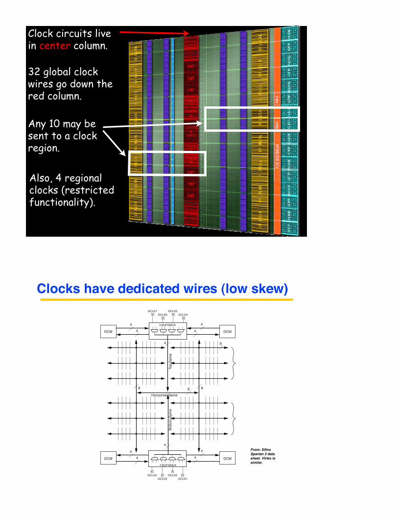
Clock circuits live in center column.
32 global clock wires go down the red column.
Also, 4 regional clocks (restricted functionality).
Any 10 may be sent to a clock region.
Clocks have dedicated wires (low skew)
Spartan-3 FPGA Family: Functional Description
30 www.xilinx.com DS099-2 (v1.3) August 24, 2004Preliminary Product Specification
40
R
width of the die. In turn, the horizontal spine branches out into a subsidiary clock interconnect that accesses the CLBs.
2. The clock input of either DCM on the same side of the die — top or bottom — as the BUFGMUX element in use.
A Global clock input is placed in a design using either aBUFGMUX element or the BUFG (Global Clock Buffer) ele-ment. For the purpose of minimizing the dynamic power dis-sipation of the clock network, the Xilinx developmentsoftware automatically disables all clock line segments thata design does not use.
Figure 18: Spartan-3 Clock Network (Top View)
4
4
4
4
4
4
4
8
8
4
4
88
Horizontal Spine
Top
Spi
neB
otto
m S
pine
4
DCM DCM
DCM DCM
Array Dependent
Array Dependent
•
•
•
•
•
•
•
•
•
•
•
•
DS099-2_18_070203
4 BUFGMUX
GCLK2GCLK3
GCLK0GCLK1
4 BUFGMUX
GCLK6 GCLK4GCLK7 GCLK5
From: Xilinx Spartan 3 data sheet. Virtex issimilar.
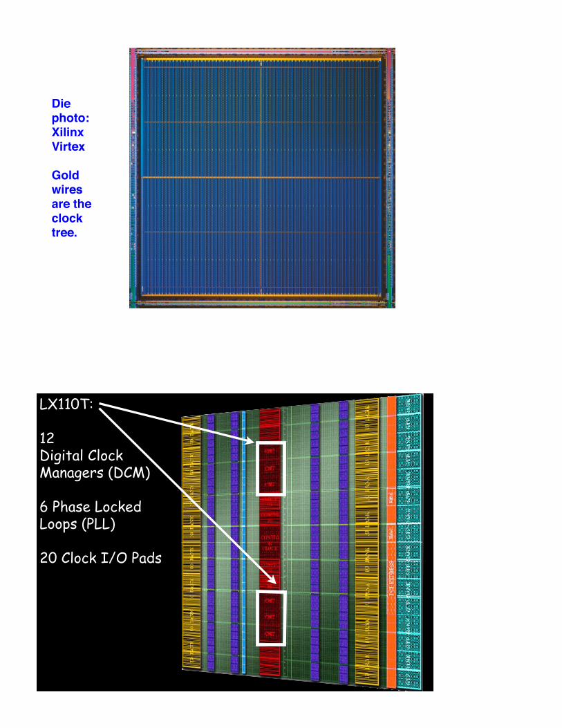
Diephoto:XilinxVirtex
Gold wiresare the clock tree.
UC Regents Fall 2008 © UCBCS 194-6 L6: Timing
!"#$%&'()*$$+,,-$$$).'/0$1
!"#$%&'&()*+#',$#-$./0123.445+6)*+#'7/4&6+-+6$0#895)($12#6: .(6;+*&6*9(&<
!"#$%&'()*!"#$%&'( !"#$%&')
LX110T:
12 Digital Clock Managers (DCM)
6 Phase Locked Loops (PLL)
20 Clock I/O Pads
DCM: Clock deskew, clock phasing
80 www.xilinx.com Virtex-5 FPGA User GuideUG190 (v4.3) September 23, 2008
Chapter 2: Clock Management TechnologyR
DCM Timing ModelsThe following timing diagrams describe the behavior of the DCM clock outputs under four different conditions:
1. Reset/Lock
2. Fixed-Phase Shifting
3. Variable-Phase Shifting
4. Status Flags
Reset/LockIn Figure 2-17, the DCM is already locked. After the reset signal is applied, all output clocks are stabilized to the desired values, and the LOCKED signal is asserted.
! Prior to Clock Event 1
Prior to clock event 1, the DCM is locked. All clock outputs are in phase with the correct frequency and behavior.
! Clock Event 1
Some time after clock event 1 the reset signal is asserted at the (RST) pin. While reset is asserted, all clock outputs become a logic zero. The reset signal is an asynchronous reset. Note: the diagram is not shown to scale. For the DCM to operate properly, the reset signal must be asserted for at least three CLKIN periods.
! Clock Event 2
Clock event 2 occurs a few cycles after reset is asserted and deasserted. At clock event 2, the lock process begins. At time LOCK_DLL, after clock event 2, if no fixed phase
Figure 2-17: RESET/LOCK Example
CLKIN
RST
CLK0
CLK90
CLK180
CLKFX
CLKFX180
CLKDV
LOCKED
1 2
3 Periods
LOCK DLL ug190_2_18_042406
46 www.xilinx.com Virtex-5 FPGA User GuideUG190 (v4.3) September 23, 2008
Chapter 2: Clock Management TechnologyR
DCM PrimitivesThe DCM primitives DCM_BASE and DCM_ADV are shown in Figure 2-2.
DCM_BASE PrimitiveThe DCM_BASE primitive accesses the basic frequently used DCM features and simplifies the user-interface ports. The clock deskew, frequency synthesis, and fixed-phase shifting features are available to use with DCM_BASE. Table 2-2 lists the available ports in the DCM_BASE primitive.
Figure 2-2: DCM Primitives
CLKINCLKFB
RST
CLK0CLK90
CLK180CLK270
CLK2XCLK2X180
CLKDV
CLKFXCLKFX180
LOCKED
CLKINCLKFB
PSINCDECPSENPSCLK
DADDR[6:0]DI[15:0]DWEDENDCLK
RST
CLK0CLK90
CLK180CLK270
CLK2XCLK2X180
CLKDV
CLKFXCLKFX180
LOCKEDPSDONEDO[15:0]
DRDY
DCM_ADVDCM_BASE
ug190_2_02_042706
Table 2-2: DCM_BASE Primitive
Available Ports Port Names
Clock Input CLKIN, CLKFB
Control and Data Input RST
Clock Output CLK0, CLK90, CLK180, CLK270, CLK2X, CLK2X180, CLKDV, CLKFX, CLKFX180
Status and Data Output LOCKED
DCM adjusts its output delay to synchronize the clock signal at the feedback clock input (CLKFB) to the clock signal at the input clock (CLKIN).
Important use is in “deskewing” on-chip clock distribution relative to input(board level) clock signal.
How it works: Delay-line feedback
Virtex-5 FPGA User Guide www.xilinx.com 71UG190 (v4.3) September 23, 2008
Application ExamplesR
Application ExamplesThe Virtex-5 FPGA DCM can be used in a variety of creative and useful applications. The following examples show some of the more common applications.
Standard UsageThe circuit in Figure 2-8 shows DCM_BASE implemented with internal feedback and access to RST and LOCKED pins. This example shows the simplest use case for a DCM.
Board-Level Clock GenerationThe board-level clock generation example in Figure 2-9 illustrates how to use a DCM to generate output clocks for other components on the board. This clock can then be used to interface with other devices. In this example, a DDR register is used with its inputs connected to GND and VCC. Because the output of the DCM is routed to BUFG, the clock stays within global routing until it reaches the output register. The quality of the clock is maintained.
The board-level clock generation example in Figure 2-10, with internal feedback, illustrates the clock generation for a forwarded clock on the board.
Figure 2-8: Standard Usage
CLKINCLK0
CLK90CLK180CLK270CLK2X
CLK2X180CLKDVCLKFX
CLKFX180
LOCKED
CLKFB
RST
IBUFGDCM_BASE
IBUF
BUFG
OBUF
ug190_2_08_032506
Virtex-5 FPGA User Guide www.xilinx.com 59UG190 (v4.3) September 23, 2008
DCM Design GuidelinesR
DCM Design GuidelinesThis section provides a detailed description on using the Virtex-5 FPGA DCM and design guidelines.
Clock DeskewThe Virtex-5 FPGA DCM offers a fully digital, dedicated, on-chip clock deskew. The deskew feature provides zero propagation delay between the source clock and output clock, low clock skew among output clock signals distributed throughout the device, and advanced clock domain control.
The deskew feature also functions as a clock mirror of a board-level clock serving multiple devices. This is achieved by driving the CLK0 output off-chip to the board (and to other devices on the board) and then bringing the clock back in as a feedback clock. See the “Application Examples” section. Taking advantage of the deskew feature greatly simplifies and improves system-level design involving high-fanout, high-performance clocks.
Clock Deskew Operation
The deskew feature utilizes the DLL circuit in the DCM. In its simplest form, the DLL consists of a single variable delay line (containing individual small delay elements or buffers) and control logic. The incoming clock drives the delay line. The output of every delay element represents a version of the incoming clock (CLKIN) delayed at a different point. The clock distribution network routes the clock to all internal registers and to the clock feedback CLKFB pin. The control logic contains a phase detector and a delay-line selector. The phase detector compares the incoming clock signal (CLKIN) against a feedback input (CLKFB) and steers the delay-line selector, essentially adding delay to the DCM output until the CLKIN and CLKFB coincide, putting the two clocks 360° out-of-phase, (thus, in phase). When the edges from the input clock line up with the edges from the feedback clock, the DCM achieves a lock. The two clocks have no discernible difference. Thus, the DCM output clock compensates for the delay in the clock distribution network, effectively removing the delay between the source clock and its loads. The size of each intrinsic delay element is a DCM_TAP (see the AC Characteristics table in the Virtex-5 FPGA Data Sheet). Figure 2-3 illustrates a simplified DLL circuit.
To provide the correct clock deskew, the DCM depends on the dedicated routing and resources used at the clock source and feedback input. An additional delay element (see “Deskew Adjust”) is available to compensate for the clock source or feedback path. The Xilinx ISE tools analyze the routing around the DCM to determine if a delay must be
Figure 2-3: Simplified DLL Circuit
ClockDistribution
NetworkVariable
Delay LineCLKOUT
Control
CLKFB
CLKIN
ug190_2_03_032506


![FAN7711 Ballast Control Integrated Circuit - Digi-Key Sheets/Fairchild PDFs/FAN7711.pdf · FAN7711 Ballast Control Integrated Circuit) 1 3 0 circuit [.] ...](https://static.fdocument.org/doc/165x107/5acfdb947f8b9a1d328d8e40/fan7711-ballast-control-integrated-circuit-digi-key-sheetsfairchild-pdfsfan7711pdffan7711.jpg)