SMD Type MOSFET - KEXIN
4
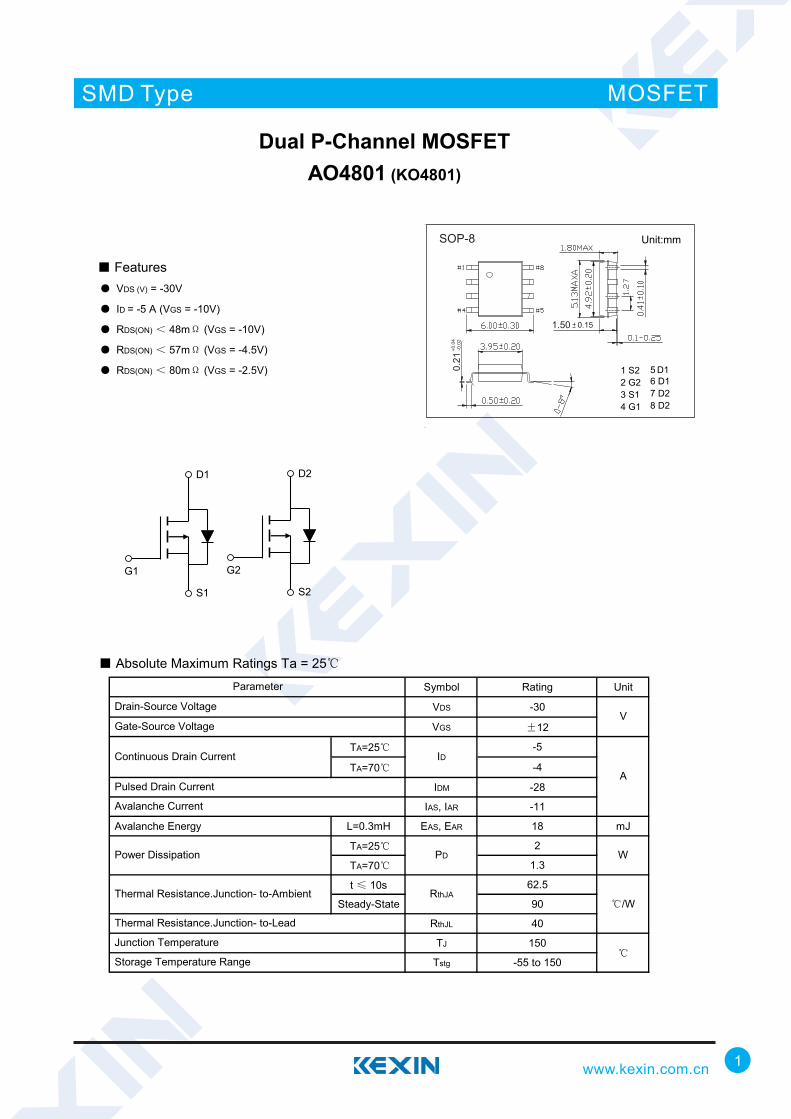
SMD Type www.kexin.com.cn 1 MOSFET Dual P-Channel MOSFET AO4801 (KO4801) ■ Features ● VDS (V) = -30V ● ID = -5 A (VGS = -10V) ● RDS(ON) < 48mΩ (VGS = -10V) ● RDS(ON) < 57mΩ (VGS = -4.5V) ● RDS(ON) < 80mΩ (VGS = -2.5V) SOP-8 0.21 +0.04 -0.02 1.50 0.15 Unit:mm 1 S2 2 G2 3 S1 4 G1 5 D1 6 D1 7 D2 8 D2 ■ Absolute Maximum Ratings Ta = 25℃ Symbol Rating Unit VDS -30 VGS ±12 TA=25℃ -5 TA=70℃ -4 IDM -28 IAS, IAR -11 Avalanche Energy L=0.3mH EAS, EAR 18 mJ TA=25℃ 2 TA=70℃ 1.3 t ≤ 10s 62.5 Steady-State 90 RthJL 40 TJ 150 Tstg -55 to 150 Avalanche Current A Thermal Resistance.Junction- to-Ambient RthJA V Pulsed Drain Current Parameter Continuous Drain Current ID Drain-Source Voltage Gate-Source Voltage Junction Temperature Storage Temperature Range PD W Power Dissipation ℃/W ℃ Thermal Resistance.Junction- to-Lead G1 D1 S1 G2 D2 S2
Transcript of SMD Type MOSFET - KEXIN
SMD Type
www.kexin.com.cn 1
MOSFET
Dual P-Channel MOSFETAO4801 (KO4801)
Features VDS (V) = -30V
ID = -5 A (VGS = -10V)
RDS(ON) < 48mΩ (VGS = -10V)
RDS(ON) < 57mΩ (VGS = -4.5V)
RDS(ON) < 80mΩ (VGS = -2.5V)
SOP-8
0.21
+0.0
4-0
.02
1.50 0.15
Unit:mm
1 S2 2 G23 S14 G1
5 D1 6 D17 D28 D2
Absolute Maximum Ratings Ta = 25
Symbol Rating Unit
VDS -30
VGS ±12
TA=25 -5
TA=70 -4
IDM -28
IAS, IAR -11
Avalanche Energy L=0.3mH EAS, EAR 18 mJ
TA=25 2
TA=70 1.3
t ≤ 10s 62.5
Steady-State 90
RthJL 40
TJ 150
Tstg -55 to 150
Avalanche Current
A
Thermal Resistance.Junction- to-Ambient RthJA
V
Pulsed Drain Current
Parameter
Continuous Drain Current ID
Drain-Source Voltage
Gate-Source Voltage
Junction Temperature
Storage Temperature Range
PD W Power Dissipation
/W
Thermal Resistance.Junction- to-Lead
G1
D1
S1
G2
D2
S2
SMD Type
www.kexin.com.cn2
MOSFET
Dual P-Channel MOSFETAO4801 (KO4801)
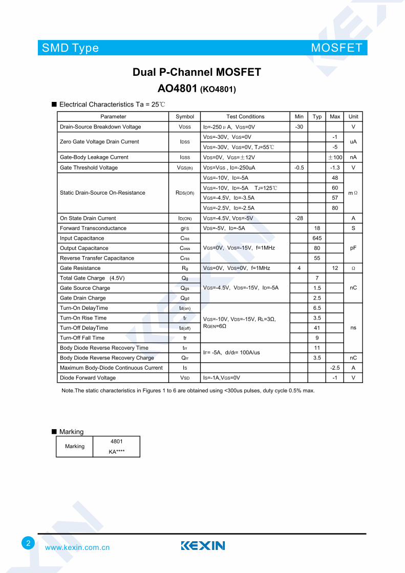
Electrical Characteristics Ta = 25
Parameter Symbol Test Conditions Min Typ Max Unit
Drain-Source Breakdown Voltage VDSS ID=-250μA, VGS=0V -30 V
VDS=-30V, VGS=0V -1
VDS=-30V, VGS=0V, TJ=55 -5
Gate-Body Leakage Current IGSS VDS=0V, VGS=±12V ±100 nA
Gate Threshold Voltage VGS(th) VDS=VGS , ID=-250uA -0.5 -1.3 V
VGS=-10V, ID=-5A 48
VGS=-10V, ID=-5A TJ=125 60
VGS=-4.5V, ID=-3.5A 57
VGS=-2.5V, ID=-2.5A 80
On State Drain Current ID(ON) VGS=-4.5V, VDS=-5V -28 A
Forward Transconductance gFS VDS=-5V, ID=-5A 18 S
Input Capacitance Ciss 645
Output Capacitance Coss 80
Reverse Transfer Capacitance Crss 55
Gate Resistance Rg VGS=0V, VDS=0V, f=1MHz 4 12 Ω
Total Gate Charge (4.5V) Qg 7
Gate Source Charge Qgs 1.5
Gate Drain Charge Qgd 2.5
Turn-On DelayTime td(on) 6.5
Turn-On Rise Time tr 3.5
Turn-Off DelayTime td(off) 41
Turn-Off Fall Time tf 9
Body Diode Reverse Recovery Time trr 11
Body Diode Reverse Recovery Charge Qrr 3.5 nC
Maximum Body-Diode Continuous Current IS -2.5 A
Diode Forward Voltage VSD IS=-1A,VGS=0V -1 V
Zero Gate Voltage Drain Current IDSS uA
mΩRDS(On) Static Drain-Source On-Resistance
VGS=-4.5V, VDS=-15V, ID=-5A
pF
nC
ns VGS=-10V, VDS=-15V, RL=3Ω, RGEN=6Ω
IF= -5A, dI/dt= 100A/us
VGS=0V, VDS=-15V, f=1MHz
Note.The static characteristics in Figures 1 to 6 are obtained using <300us pulses, duty cycle 0.5% max.
Marking4801
KA****Marking
SMD Type
www.kexin.com.cn 3
MOSFET
Dual P-Channel MOSFETAO4801 (KO4801)
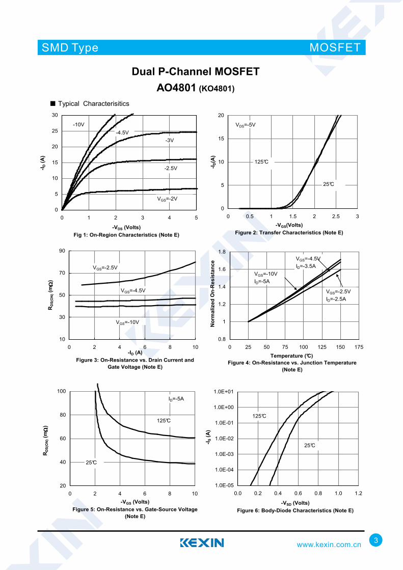
Typical Characterisitics
175
0
5
10
15
20
0 0.5 1 1.5 2 2.5 3-VGS(Volts)
Figure 2: Transfer Characteristics (Note E)
-I D(A
)
10
30
50
70
90
0 2 4 6 8 10-ID (A)
Figure 3: On-Resistance vs. Drain Current andGate Voltage (Note E)
RD
S(O
N) (
mΩΩ ΩΩ
)
1.0E-05
1.0E-04
1.0E-03
1.0E-02
1.0E-01
1.0E+00
1.0E+01
0.0 0.2 0.4 0.6 0.8 1.0 1.2
-VSD (Volts)Figure 6: Body-Diode Characteristics (Note E)
-I S (A
)
25°C
125°C
0.8
1
1.2
1.4
1.6
1.8
0 25 50 75 100 125 150 175
Temperature (°C)Figure 4: On-Resistance vs. Junction Temperature
(Note E)
Nor
mal
ized
On-
Res
ista
nce
VGS=-2.5VID=-2.5A
VGS=-10VID=-5A
VGS=-4.5VID=-3.5A
20
40
60
80
100
0 2 4 6 8 10-VGS (Volts)
Figure 5: On-Resistance vs. Gate-Source Voltage(Note E)
RD
S(O
N) (
mΩΩ ΩΩ
)
25°C
125°C
VDS=-5V
VGS=-4.5V
VGS=-10V
ID=-5A
25°C
125°C
0
5
10
15
20
25
30
0 1 2 3 4 5
-VDS (Volts)Fig 1: On-Region Characteristics (Note E)
-I D (A
)
VGS=-2V
-2.5V
-4.5V-3V
-10V
VGS=-2.5V
SMD Type
www.kexin.com.cn4
MOSFET
.
Dual P-Channel MOSFETAO4801 (KO4801)
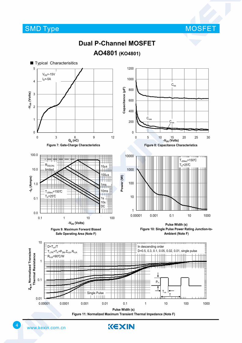
Typical Characterisitics
0.01
0.1
1
10
0.00001 0.0001 0.001 0.01 0.1 1 10 100 1000
Pulse Width (s)Figure 11: Normalized Maximum Transient Thermal Impedance (Note F)
Z θθ θθJA
Nor
mal
ized
Tra
nsie
ntTh
erm
al R
esis
tanc
e
1
10
100
1000
10000
0.00001 0.001 0.1 10 1000
Pulse Width (s)Figure 10: Single Pulse Power Rating Junction-to-
Ambient (Note F)
Pow
er (W
)
TJ(Max)=150°CTA=25°C
0
1
2
3
4
5
0 3 6 9 12Qg (nC)
Figure 7: Gate-Charge Characteristics
-VG
S (V
olts
)
0
200
400
600
800
1000
1200
0 5 10 15 20 25 30-VDS (Volts)
Figure 8: Capacitance Characteristics
Cap
acita
nce
(pF)
Ciss
CossCrss
VDS=-15VID=-5A
0.0
0.1
1.0
10.0
100.0
0.1 1 10 100-VDS (Volts)
-I D (A
mps
)
Figure 9: Maximum Forward BiasedSafe Operating Area (Note F)
10µs
10s
1ms
DC
RDS(ON)
limited
TJ(Max)=150°CTA=25°C
100µs
1s
10ms
Single Pulse
D=Ton/TTJ,PK=TA+PDM.ZθJA.RθJA
TonT
PD
In descending orderD=0.5, 0.3, 0.1, 0.05, 0.02, 0.01, single pulse
RθJA=90°C/W