Sub-threshold MOSFET Operation - MIT OpenCourseWare · PDF fileSub-threshold MOSFET Operation...
29
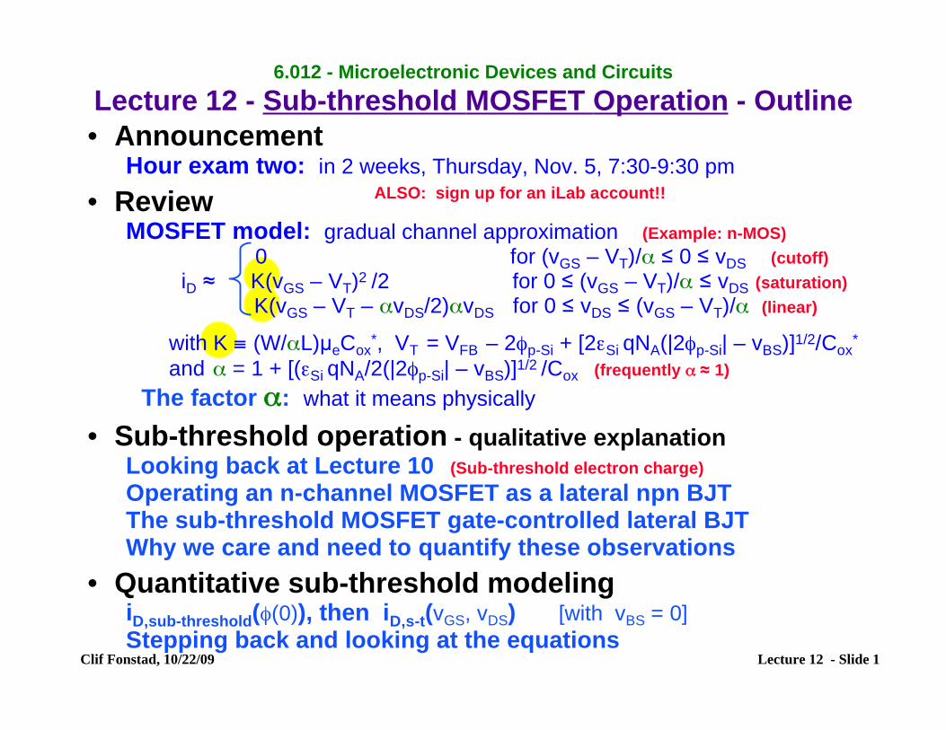
0 i D ≈ K(v GS – V T with K ≡ (W/αL)µ e 6.012 - Microelectronic Devices and Circuits Lecture 12 - Sub-threshold MOSFET Operation - Outline • Announcement Hour exam two: in 2 weeks, Thursday, Nov. 5, 7:30-9:30 pm ALSO: sign up for an iLab account!! • Review MOSFET model: gradual channel approximation (Example: n-MOS) for (v GS – V T )/α ≤ 0 ≤ v DS (cutoff) K(v GS – V T ) 2 /2 for 0 ≤ (v GS – V T )/α ≤ v DS (saturation) – αv DS /2)αv DS for 0 ≤ v DS ≤ (v GS – V T )/α (linear) * * C ox , V T = V FB –2φ p-Si + [2ε Si qN A (|2φ p-Si | – v BS )] 1/2 /C ox and α = 1 + [(ε Si qN A /2(|2φ p-Si | – v BS )] 1/2 /C ox (frequently α ≈ 1) The factor α: what it means physically • Sub-threshold operation - qualitative explanation Looking back at Lecture 10 (Sub-threshold electron charge) Operating an n-channel MOSFET as a lateral npn BJT The sub-threshold MOSFET gate-controlled lateral BJT Why we care and need to quantify these observations • Quantitative sub-threshold modeling i D,sub-threshold (φ(0)), then i D,s-t (v GS , v DS ) [with v BS = 0] Stepping back and looking at the equations Clif Fonstad, 10/22/09 Lecture 12 - Slide 1
-
Upload
dangnguyet -
Category
Documents
-
view
228 -
download
2
Transcript of Sub-threshold MOSFET Operation - MIT OpenCourseWare · PDF fileSub-threshold MOSFET Operation...
0 iD ≈
K(vGS – VT
with K ≡ (W/αL)µe
6.012 - Microelectronic Devices and Circuits Lecture 12 - Sub-threshold MOSFET Operation - Outline • Announcement
Hour exam two: in 2 weeks, Thursday, Nov. 5, 7:30-9:30 pm ALSO: sign up for an iLab account!! • Review
MOSFET model: gradual channel approximation (Example: n-MOS) for (vGS – VT)/α ≤ 0 ≤ vDS (cutoff)
K(vGS – VT)2 /2 for 0 ≤ (vGS – VT)/α ≤ vDS (saturation) – αvDS/2)αvDS for 0 ≤ vDS ≤ (vGS – VT)/α (linear)
* *Cox , VT = VFB – 2φp-Si + [2εSi qNA(|2φp-Si| – vBS)]1/2/Cox and α = 1 + [(εSi qNA/2(|2φp-Si| – vBS)]1/2 /Cox (frequently α ≈ 1)
The factor α: what it means physically
• Sub-threshold operation - qualitative explanation Looking back at Lecture 10 (Sub-threshold electron charge) Operating an n-channel MOSFET as a lateral npn BJT The sub-threshold MOSFET gate-controlled lateral BJT Why we care and need to quantify these observations
• Quantitative sub-threshold modelingiD,sub-threshold(φ(0)), then iD,s-t(vGS, vDS) [with vBS = 0] Stepping back and looking at the equations
Clif Fonstad, 10/22/09 Lecture 12 - Slide 1
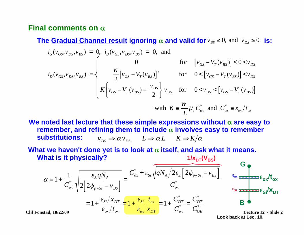
Final comments on α
The Gradual Channel result ignoring α and valid for is:
!
iG
(vGS
,vDS
,vBS
) = 0, iB(v
GS,v
DS,v
BS) = 0, and
iD
(vGS
,vDS
,vBS
) =
0 for vGS"V
T(v
BS)[ ] < 0 <v
DS
K
2v
GS"V
T(v
BS)[ ]2
for 0 < vGS"V
T(v
BS)[ ] <v
DS
K vGS"V
T(v
BS) "
vDS
2
# $ %
& ' (
vDS
for 0 <vDS
< vGS"V
T(v
BS)[ ]
with K )W
Lµ
eC
ox
* and C
ox
* ) *ox
tox
!
vBS" 0, and v
DS# 0
We noted last lecture that these simple expressions without α are easy toremember, and refining them to include α involves easy to remembersubstitutions:
!
vDS"# v
DSL "# L K "K #
What we haven't done yet is to look at α itself, and ask what it means. What is it physically?
!
" #1+1
Cox
*
$SiqN
A
2 2%p&Si
& vBS[ ]
=C
ox
* + $Si
qNA
2$Si
2%p&Si
& vBS[ ]
Cox
*
1/xDT(VBS) G
εox εox/tox
εSi
!
=1+"
Six
DT
"ox
tox
=1+"
Si
"ox
tox
xDT
=1+C
DT
*
Cox
*=
CDT
*
CGB
*
εSi/xDT
B Clif Fonstad, 10/22/09 Lecture 12 - Slide 2
Look back at Lec. 10.
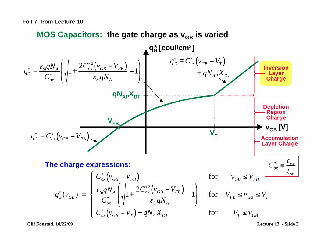
Foil 7 from Lecture 10
MOS Capacitors: the gate charge as vGB is varied
Clif Fonstad, 10/22/09 Lecture 12 - Slide 3
vGB [V] VT
VFB
qG* [coul/cm2]
qNAPXDT
!
qG
" = Cox
"v
GB#V
T( ) + qN
APX
DT
Inversion Layer
Charge
!
qG
"(v
GB) =
Cox
"v
GB#V
FB( ) for vGB$V
FB
%SiqN
A
Cox
"1+
2Cox
"2v
GB#V
FB( )%
SiqN
A
#1
&
' ( (
)
* + + for V
FB$ v
GB$V
T
Cox
"v
GB#V
T( ) + qNAX
DT for V
T$ v
GB
,
-
.
.
/
.
.
The charge expressions:
!
qG
" =#
SiqN
A
Cox
"1+
2Cox
"2v
GB$V
FB( )#
SiqN
A
$1
%
& ' '
(
) * *
DepletionRegionCharge
!
qG
" = Cox
"v
GB#V
FB( ) Accumulation Layer Charge
!
Cox
"#$
ox
tox
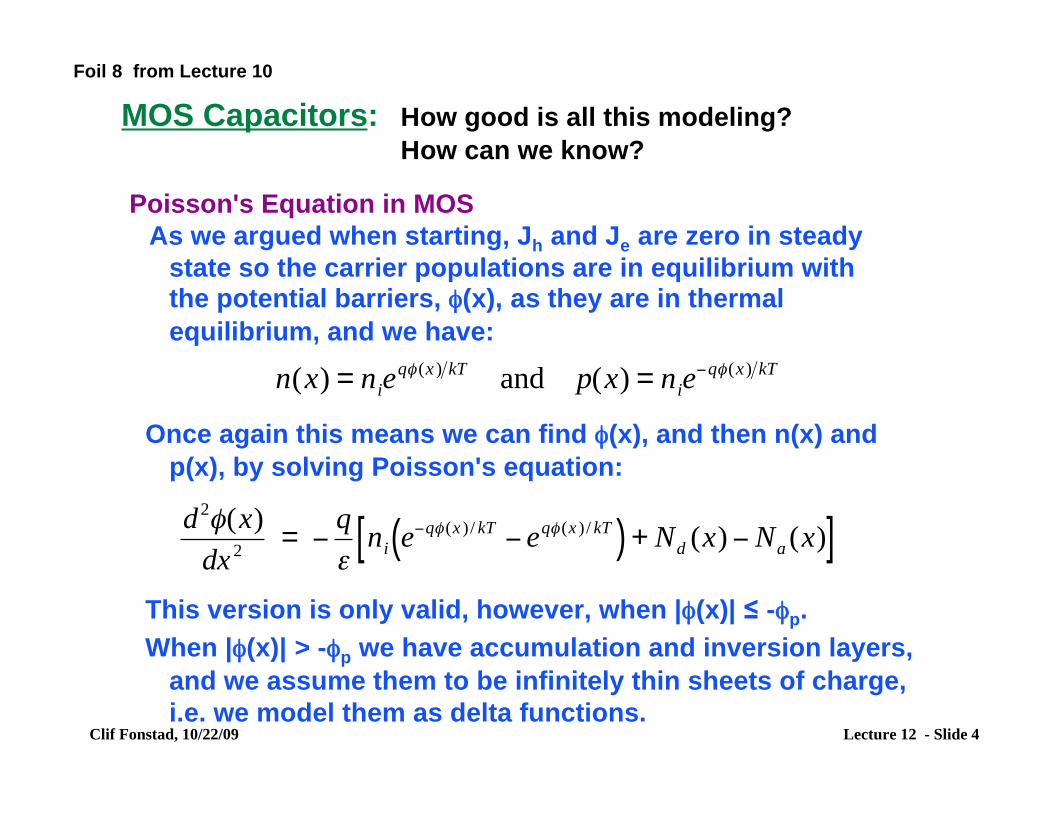
Foil 8 from Lecture 10
MOS Capacitors: How good is all this modeling? How can we know?
Poisson's Equation in MOS As we argued when starting, Jh and Je are zero in steady
state so the carrier populations are in equilibrium with the potential barriers, φ(x), as they are in thermal equilibrium, and we have:
!
n(x) = nie
q" (x ) kTand p(x) = n
ie#q" (x ) kT
Once again this means we can find φ(x), and then n(x) and p(x), by solving Poisson's equation:
!
d2"(x)
dx2
= #q
$n
ie#q" (x ) / kT # e
q" (x ) / kT( ) + Nd(x) # N
a(x)[ ]
This version is only valid, however, when |φ(x)| ≤ -φp. When |φ(x)| > -φp we have accumulation and inversion layers,
and we assume them to be infinitely thin sheets of charge, i.e. we model them as delta functions.
Clif Fonstad, 10/22/09 Lecture 12 - Slide 4
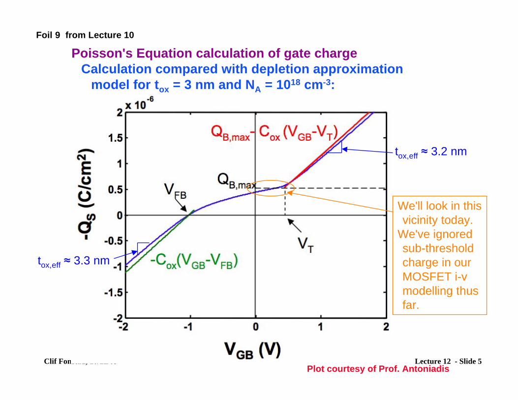
Foil 9 from Lecture 10
Poisson's Equation calculation of gate charge Calculation compared with depletion approximation
model for tox = 3 nm and NA = 1018 cm-3:
Clif Fonstad, 10/22/09 Lecture 12 - Slide 5
tox,eff ≈ 3.3 nm
tox,eff ≈ 3.2 nm
We'll look in this vicinity today.
We've ignored sub-threshold charge in our MOSFET i-v modelling thus far.
Plot courtesy of Prof. Antoniadis
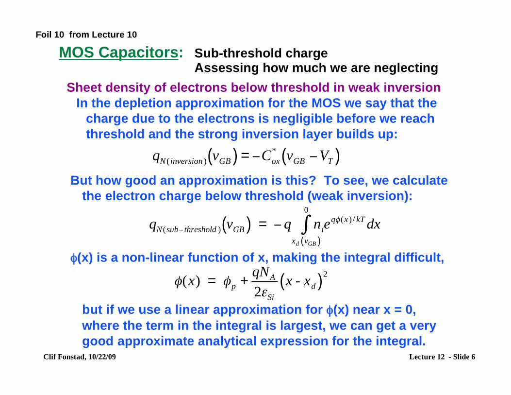
Foil 10 from Lecture 10
MOS Capacitors: Sub-threshold chargeAssessing how much we are neglecting
Sheet density of electrons below threshold in weak inversion In the depletion approximation for the MOS we say that the
charge due to the electrons is negligible before we reach threshold and the strong inversion layer builds up:
!
qN ( inversion ) v
GB( ) = "Cox
*v
GB"V
T( )But how good an approximation is this? To see, we calculate
the electron charge below threshold (weak inversion):
!
qN (sub" threshold ) v
GB( ) = " q nie
q# (x ) / kTdx
xd
vGB( )
0
$
φ(x) is a non-linear function of x, making the integral difficult,
!
"(x) = "p
+qN
A
2#Si
x - xd( )2
but if we use a linear approximation for φ(x) near x = 0, where the term in the integral is largest, we can get a very good approximate analytical expression for the integral.
Clif Fonstad, 10/22/09 Lecture 12 - Slide 6
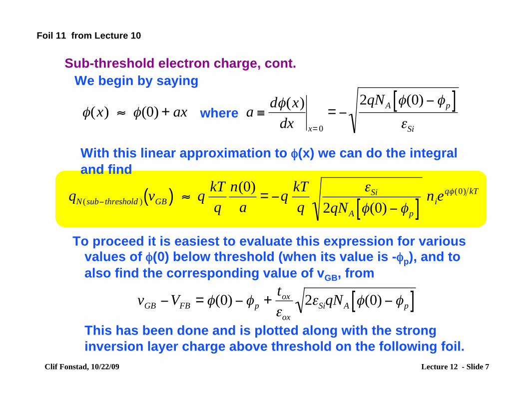
Foil 11 from Lecture 10
Sub-threshold electron charge, cont. We begin by saying
!
"(x) # "(0) + ax where a $d"(x)
dxx= 0
= %2qN
A"(0) %"
p[ ]&
Si
where
With this linear approximation to φ(x) we can do the integral and find
!
qN (sub" threshold ) v
GB( ) # qkT
q
n(0)
a= "q
kT
q
$Si
2qNA%(0) "%
p[ ]n
ie
q% (0) kT
To proceed it is easiest to evaluate this expression for various values of φ(0) below threshold (when its value is -φp), and to also find the corresponding value of vGB, from
!
vGB"V
FB= #(0) "#
p+
tox
$ox
2$SiqN
A#(0) "#
p[ ]This has been done and is plotted along with the strong inversion layer charge above threshold on the following foil.
Clif Fonstad, 10/22/09 Lecture 12 - Slide 7
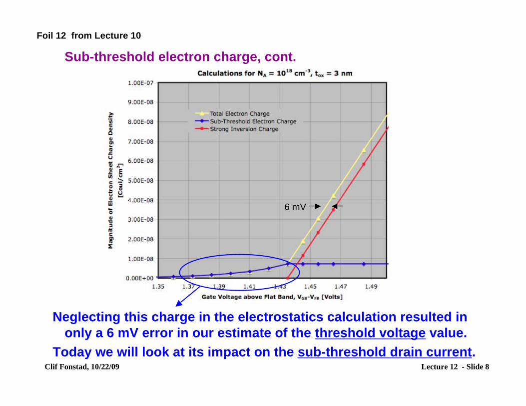
Foil 12 from Lecture 10
Sub-threshold electron charge, cont.
6 mV
Neglecting this charge in the electrostatics calculation resulted in only a 6 mV error in our estimate of the threshold voltage value.
Today we will look at its impact on the sub-threshold drain current. Clif Fonstad, 10/22/09 Lecture 12 - Slide 8
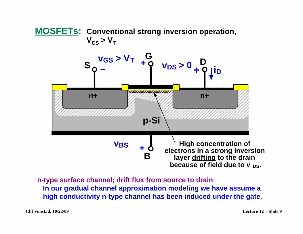
MOSFETs: Conventional strong inversion operation,VGS > VT
p-Si
B
G+
vGS > VT
n+
D
n+
S – vDS > 0
vBS +
iD
High concentration of electrons in a strong inversion
layer drifting to the drain because of field due to v DS.
n-type surface channel; drift flux from source to drain In our gradual channel approximation modeling we have assume a high conductivity n-type channel has been induced under the gate.
Clif Fonstad, 10/22/09 Lecture 12 - Slide 9
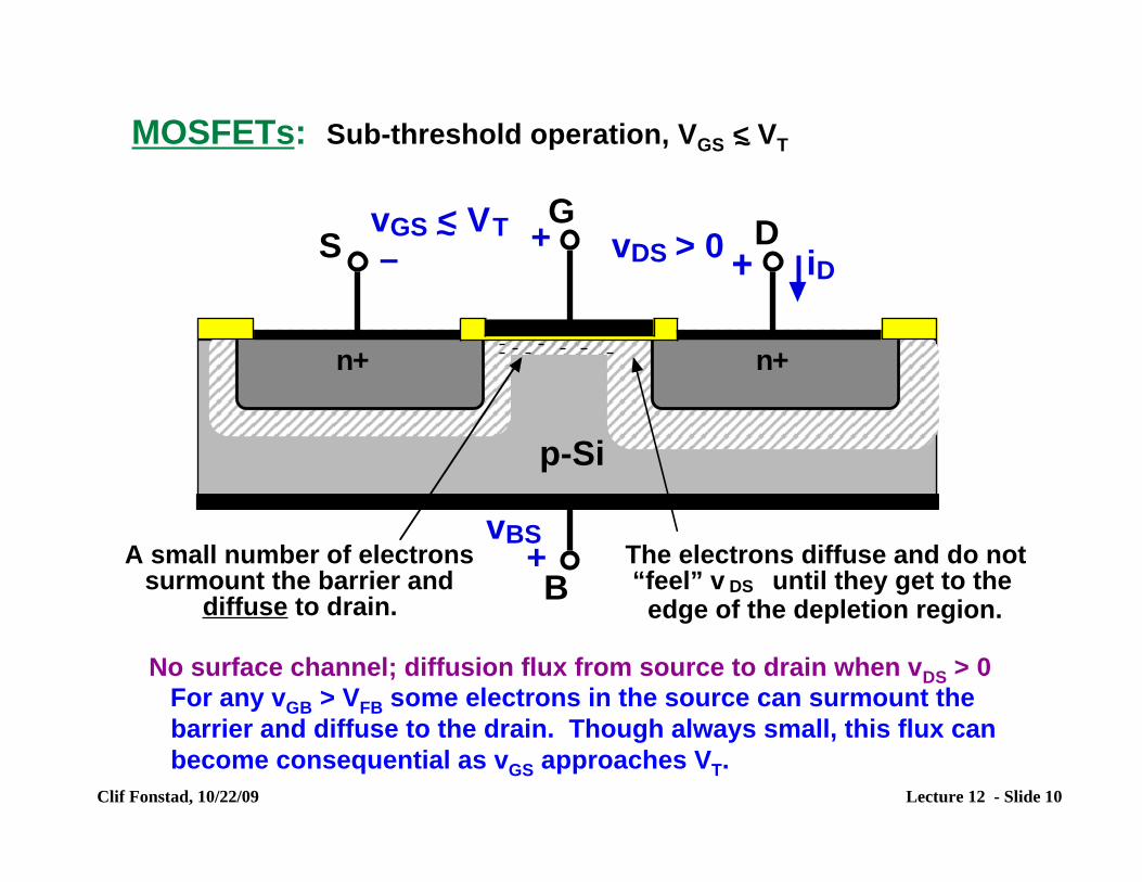
MOSFETs: Sub-threshold operation, VGS < VT~
p-Si
B
G+
vGS < VT
n+
D
n+
S – vDS > 0
vBS+
iD
A small number of electrons surmount the barrier and
diffuse to drain.
~
The electrons diffuse and do not “feel” v DS until they get to the
edge of the depletion region.
No surface channel; diffusion flux from source to drain when vDS > 0 For any vGB > VFB some electrons in the source can surmount the barrier and diffuse to the drain. Though always small, this flux can become consequential as vGS approaches VT.
Clif Fonstad, 10/22/09 Lecture 12 - Slide 10
MOSFETs: Sub-threshold operation, VGS < VT~ What do we mean by "consequential"?
When is this current big enough to matter? There are at least three places where it matters:
1. It can limit the gain of a MOSFET linear amplifier. In Lecture 21 we will learn that we achieve maximum gain from MOSFETs operating in strong inversion when we bias as close to threshold as possible. This current limits how close we can get.
2. It is a major source of power dissipation and heating in modern VLSI digital ICs. When you have millions of MOSFETs on an IC chip, even a little bit of current through the half that are supposed to be "off" can add up to a lot of power dissipation. We'll see this in Lecture 16.
3. It can be used to make very low voltage, ultra-low power integrated circuits. In Lecture 25 we'll talk about MIT/TI research on sub-threshold circuits with 0.3 V supplies and using µW's of power.
Clif Fonstad, 10/22/09 Lecture 12 - Slide 11
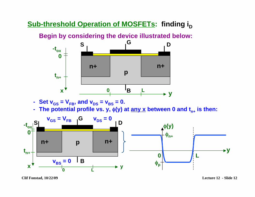
Sub-threshold Operation of MOSFETs: finding iD
Begin by considering the device illustrated below: D
B
S G
n+ n+ p
-tox
tn+
0
x y0 L
- Set vGS = VFB, and vDS = vBS = 0. - The potential profile vs. y, φ(y) at any x between 0 and tn+ is then:
vGS = VFB G vDS = 0S
n+ n+ p
D-tox
0
tn+
vBS = 0 B
φ(y)
φn+
0 L φp
y
y0 L
Clif Fonstad, 10/22/09 Lecture 12 - Slide 12
x
φ(y)
φn+
φp
φn++ vDS
0 L
vDS
Sub-threshold Operation of MOSFETs, cont.
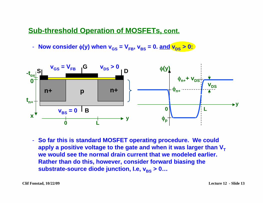
- Now consider φ(y) when vGS = VFB, vBS = 0. and vDS > 0:
n+ n+ p
vGS = VFB G vDS > 0S D-tox
0
tn+ y
vBS = 0 B x y
0 L
- So far this is standard MOSFET operating procedure. We could apply a positive voltage to the gate and when it was larger than VT we would see the normal drain current that we modeled earlier. Rather than do this, however, consider forward biasing the substrate-source diode junction, I.e, vBS > 0…
Clif Fonstad, 10/22/09 Lecture 12 - Slide 13
+ vBS.
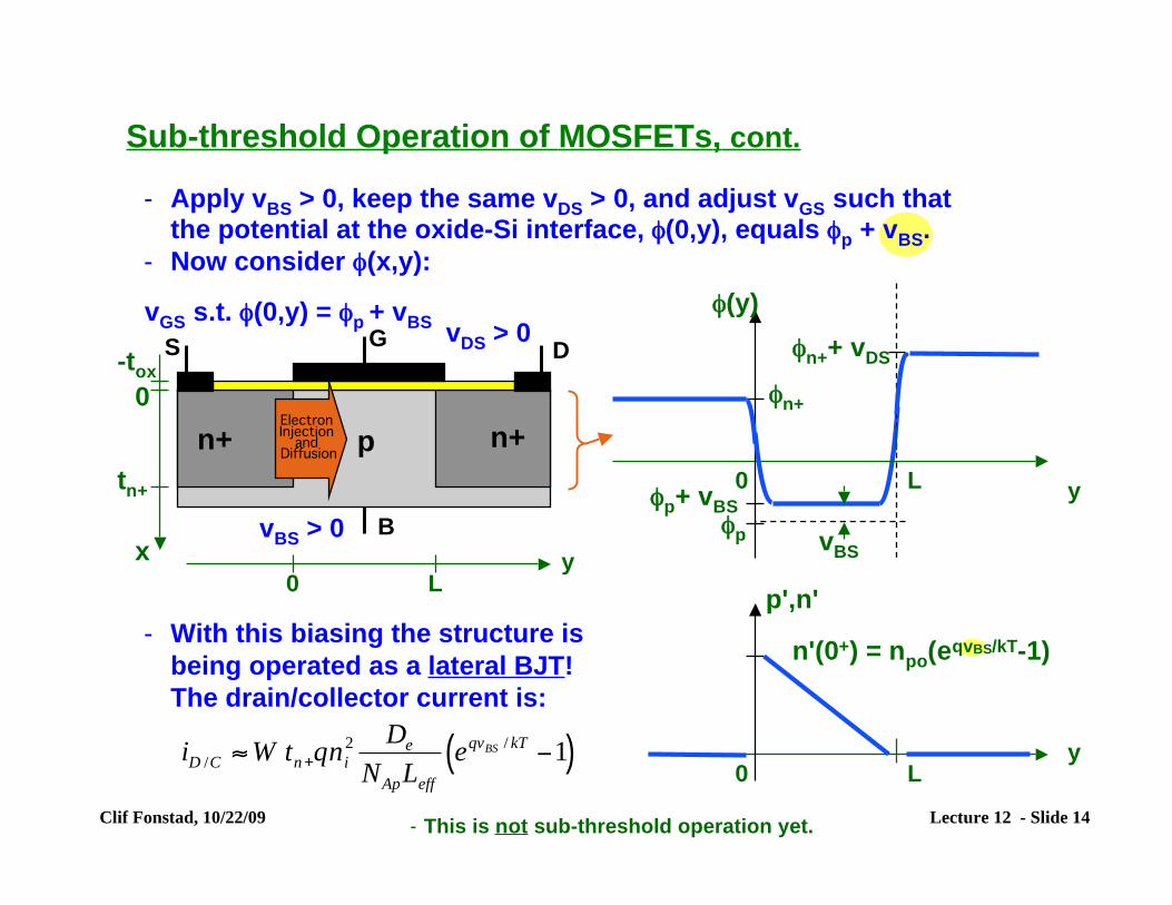
Sub-threshold Operation of MOSFETs, cont.
- Apply vBS > 0, keep the same vDS > 0, and adjust vGS such that the potential at the oxide-Si interface, φ(0,y), equals φp
- Now consider φ(x,y): φ(y) vGS s.t. φ(0,y) = φp + vBS
G vDS > 0S
n+ n+ p Electron Injection
and Diffusion
D φn++ vDS -tox
0 φn+
0 Ltn+ yφp+ vBS
B φpx
vBS > 0 vBS
y0 L
p',n'
- With this biasing the structure is being operated as a lateral BJT! The drain/collector current is:
!
iD /C "W t
n +qni
2 De
NAp
Leff
eqv
BS/ kT#1( )
0 L
n'(0+) = npo(eqvBS/kT-1)
y
Clif Fonstad, 10/22/09 Lecture 12 - Slide 14 - This is not sub-threshold operation yet.
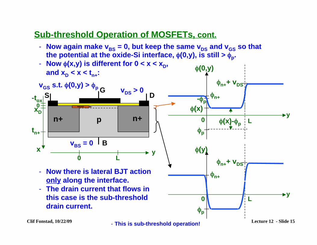
Sub-threshold Operation of MOSFETs, cont.
- Now again make vBS = 0, but keep the same vDS and vGS so that the potential at the oxide-Si interface, φ(0,y), is still > φp.
- Now φ(x,y) is different for 0 < x < xD, and xD < x < tn+:
vGS s.t. φ(0,y) > φp
n+ n+ p
Injection
G vDS > 0S D-tox
0xD y
tn+
vBS = 0 B x
0 L
- Now there is lateral BJT action only along the interface.
- The drain current that flows in ythis case is the sub-threshold
drain current.
y φ(y)
φn+
φp
φn++ vDS
0 L
φ(0,y)
φn+
φp
φn++ vDS
0 L
φ(x)
φ(x)-φp
-φp
Clif Fonstad, 10/22/09 Lecture 12 - Slide 15 - This is sub-threshold operation!
x
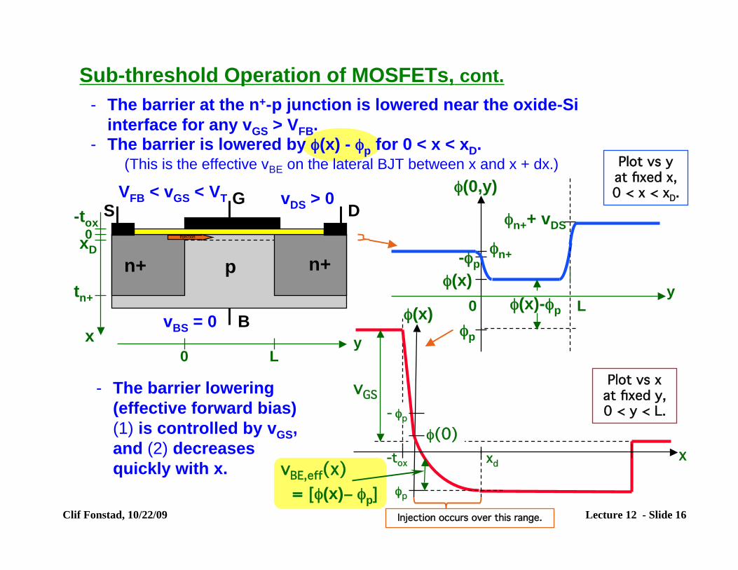
Sub-threshold Operation of MOSFETs, cont. - The barrier at the n+-p junction is lowered near the oxide-Si
interface for any vGS > VFB. - The barrier is lowered by φ(x) - φp for 0 < x < xD.
(This is the effective vBE on the lateral BJT between x and x + dx.) Plot vs y at fixed x,
S-tox 0
Clif Fonstad, 10/22/09 Lecture 12 - Slide 16
The barrier lowering (effective forward bias) (1) is controlled by vGS, and (2) decreases quickly with x.
D
B
G
n+ n+ p
tn+
y0 L
vBS = 0
vDS > 0
Injection
VFB < vGS < VT 0 < x < xD.
- φp
φ(0)
φ
-tox vBE,eff(x)p
xd
vGS
= [φ(x)− φp]
Plot vs x at fixed y, 0 < y < L.
φ(x)
Injection occurs over this range.
y
φn+
φp
φn++ vDS
0
φ(0,y)
L
φ(x)
φ(x)-φp
-φp
xD
-
x
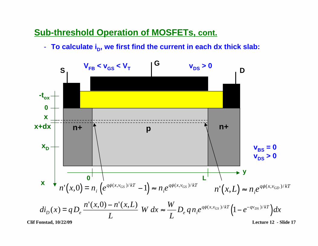
Sub-threshold Operation of MOSFETs, cont. - To calculate iD, we first find the current in each dx thick slab:
DS G
-tox
0
x
y0 L
vDS > 0
xD
VFB < vGS < VT
n+ n+ p
x
x+dx
!
n' x,0( ) = ni
eq" (x,v
GS) / kT #1( ) $ n
ie
q" (x,vGS
) / kT
vBS = 0 vDS > 0
!
n' x,L( ) " nie
q# (x,vGD
) / kT
!
diD(x) = qD
e
n'(x,0) " n'(x,L)
LW dx #
W
LD
eqn
ie
q$ (x,vGS
) / kT1" e
"qvDS
) / kT( )dx
Clif Fonstad, 10/22/09 Lecture 12 - Slide 17
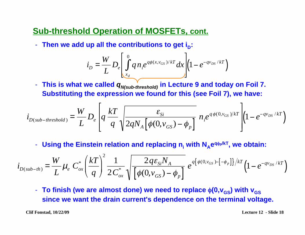
Sub-threshold Operation of MOSFETs, cont. - Then we add up all the contributions to get iD:
!
iD
=W
LD
eqn
ie
q" (x,vGS
) / kTdx
xd
0
#$
% & &
'
( ) )
1* e*qv
DS/ kT( )
- This is what we called qN(sub-threshold) in Lecture 9 and today on Foil 7. Substituting the expression we found for this (see Foil 7), we have:
!
iD(sub" threshold ) =
W
LD
eq
kT
q
#Si
2qNA$(0,v
GS) "$
p[ ]n
ie
q$ (0,vGS
) kT
%
& ' '
(
) * *
1" e"qv
DS/ kT( )
- Using the Einstein relation and replacing ni with NAeqφp/kT, we obtain:
!
iD(sub" th ) =
W
Lµ
eC
ox
* kT
q
#
$ %
&
' (
2
1
2Cox
*
2q)SiN
A
*(0,vGS
) "*p[ ]
eq * (0,v
GS)" "*
p[ ]{ } kT
1" e"qv
DS/ kT( )
- To finish (we are almost done) we need to replace φ(0,vGS) with vGS since we want the drain current's dependence on the terminal voltage.
Clif Fonstad, 10/22/09 Lecture 12 - Slide 18
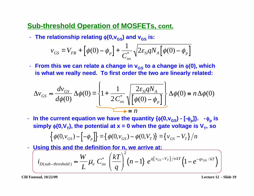
Sub-threshold Operation of MOSFETs, cont. - The relationship relating φ(0,vGS) and vGS is:
!
vGS
= VFB
+ "(0) #"p[ ] +
1
Cox
*2$
SiqN
A"(0) #"
p[ ]- From this we can relate a change in vGS to a change in φ(0), which
is what we really need. To first order the two are linearly related:
!
"vGS#
dvGS
d$(0)"$(0) = 1+
1
2Cox
*
2%SiqN
A
$(0) &$p[ ]
' ( )
* )
+ , )
- ) "$(0) . n"$(0)
!
" n
- In the current equation we have the quantity {φ(0,vGS) - [-φp]}. -φp is simply φ(0,VT), the potential at x = 0 when the gate voltage is VT, so
!
"(0,vGS
) # #"p[ ]{ } = "(0,v
GS) #"(0,V
T){ } = v
GS#V
T{ } n
!
iD(sub" threshold ) #
W
Lµ
eC
ox
* kT
q
$
% &
'
( )
2
n "1( ) eq v
GS"V
T{ } n kT
1" e"qv
DS/ kT( )
- Using this and the definition for n, we arrive at:
Clif Fonstad, 10/22/09 Lecture 12 - Slide 19
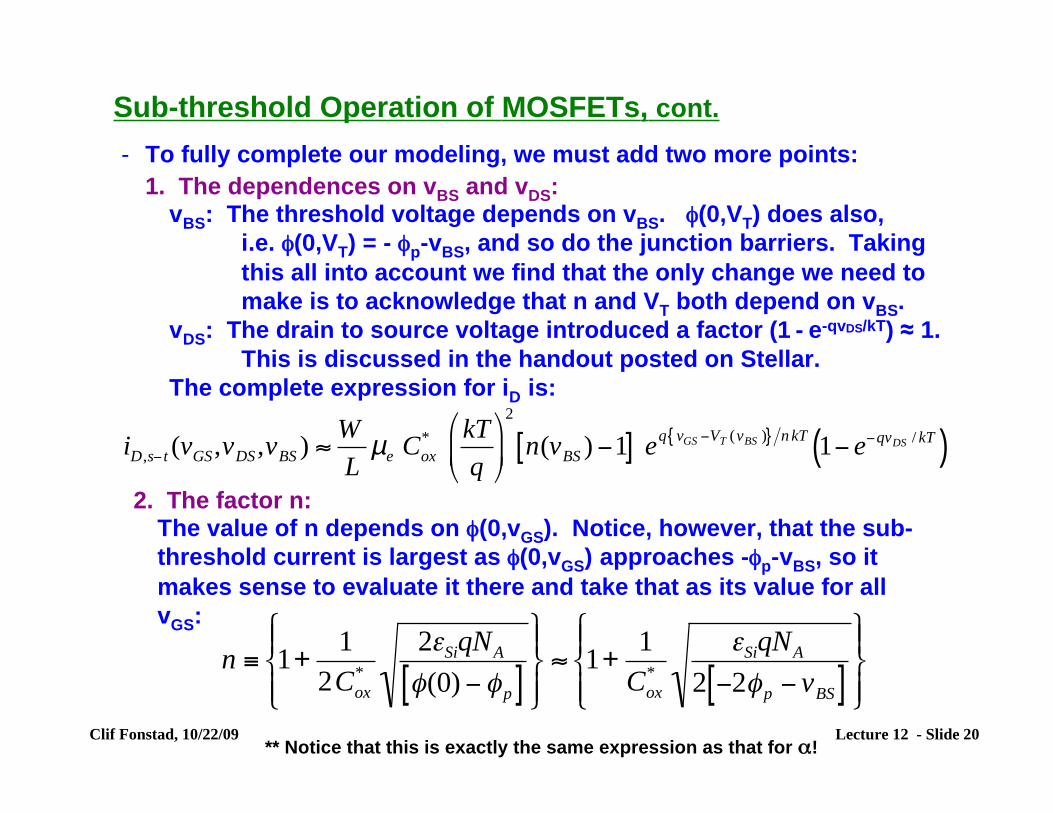
Sub-threshold Operation of MOSFETs, cont. - To fully complete our modeling, we must add two more points:
1. The dependences on vBS and vDS: vBS: The threshold voltage depends on vBS. φ(0,VT) does also,
i.e. φ(0,VT) = - φp-vBS, and so do the junction barriers. Taking this all into account we find that the only change we need to make is to acknowledge that n and VT both depend on vBS.
vDS: The drain to source voltage introduced a factor (1 - e-qvDS/kT) ≈ 1. This is discussed in the handout posted on Stellar.
!
iD,s" t
(vGS
,vDS
,vBS
) #W
Lµ
eC
ox
* kT
q
$
% &
'
( )
2
n(vBS
) "1[ ] eq v
GS"V
T(v
BS){ } n kT
1" e"qv
DS/ kT( )
The complete expression for iD is:
2. The factor n: The value of n depends on φ(0,vGS). Notice, however, that the sub-threshold current is largest as φ(0,vGS) approaches -φp-vBS, so it makes sense to evaluate it there and take that as its value for all
!
n " 1+1
2Cox
*
2#SiqN
A
$(0) %$p[ ]
& ' (
) (
* + (
, ( - 1+
1
Cox
*
#SiqN
A
2 %2$p% v
BS[ ]& ' (
) (
* + (
, (
vGS:
Clif Fonstad, 10/22/09 Lecture 12 - Slide 20 ** Notice that this is exactly the same expression as that for α!
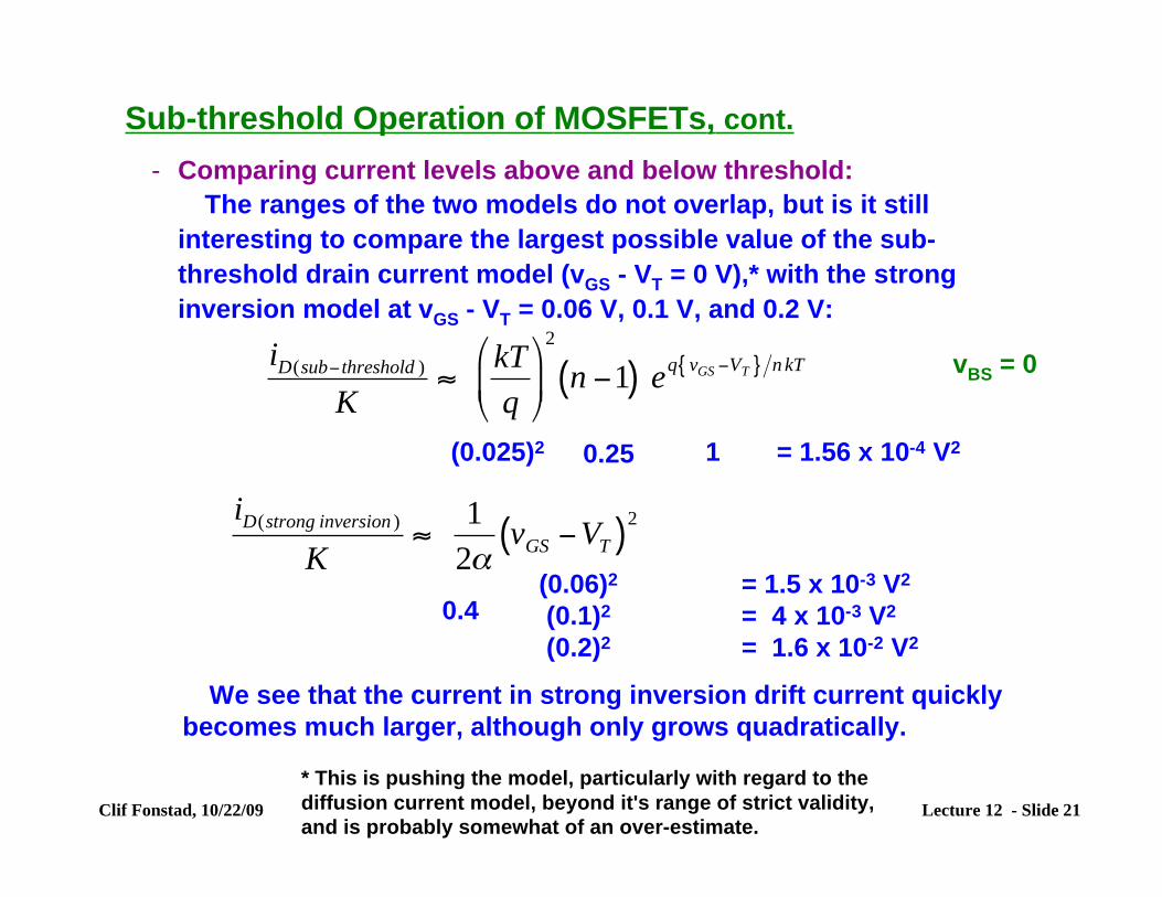
Sub-threshold Operation of MOSFETs, cont. - Comparing current levels above and below threshold:
The ranges of the two models do not overlap, but is it still interesting to compare the largest possible value of the sub-threshold drain current model (vGS - VT = 0 V),* with the strong inversion model at vGS - VT = 0.06 V, 0.1 V, and 0.2 V:
!
iD(sub" threshold )
K#
kT
q
$
% &
'
( )
2
n "1( ) eq v
GS"V
T{ } n kT vBS = 0
(0.025)2 0.25 1 = 1.56 x 10⁻⁴ V2
!
iD(strong inversion )
K"
1
2#v
GS$V
T( )2
(0.06)2 = 1.5 x 10⁻³ V2
0.4 (0.1)2 = 4 x 10⁻³ V2
(0.2)2 = 1.6 x 10⁻² V2
We see that the current in strong inversion drift current quickly becomes much larger, although only grows quadratically.
* This is pushing the model, particularly with regard to the diffusion current model, beyond it's range of strict validity, Clif Fonstad, 10/22/09 Lecture 12 - Slide 21 and is probably somewhat of an over-estimate.
Clif Fonstad, 10/22/09 Lecture 12 - Slide 22
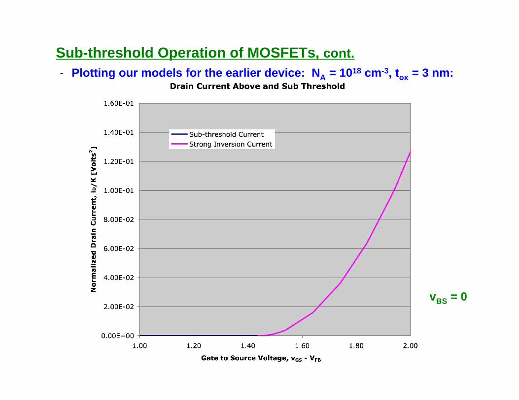
Sub-threshold Operation of MOSFETs, cont. - Plotting our models for the earlier device: NA = 1018 cm-3, tox = 3 nm:
vBS = 0
Clif Fonstad, 10/22/09 Lecture 12 - Slide 23
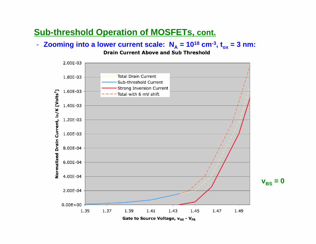
Sub-threshold Operation of MOSFETs, cont. - Zooming into a lower current scale: NA = 1018 cm-3, tox = 3 nm:
vBS = 0
Lecture 12 - Slide 2
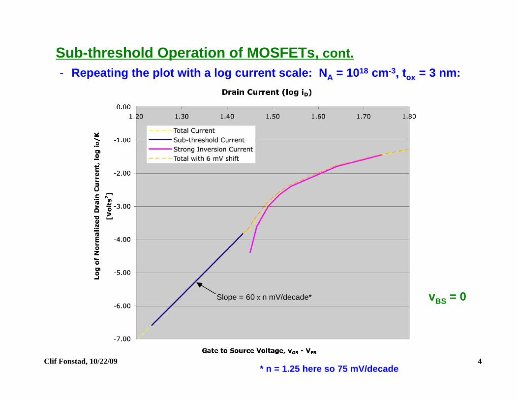
Sub-threshold Operation of MOSFETs, cont. - = 3 nm:
* n = 1.25 here so 75 mV/decade Clif Fonstad, 10/22/09 4
Repeating the plot with a log current scale: NA = 1018 cm-3, tox
Slope = 60 x n mV/decade* vBS = 0
Sub-threshold Output Characteristic
!
IS,s" t
#W
Lµ
eC
ox
* kT
q
$
% &
'
( )
2
n "1[ ] = KoV
t
2n "1[ ]
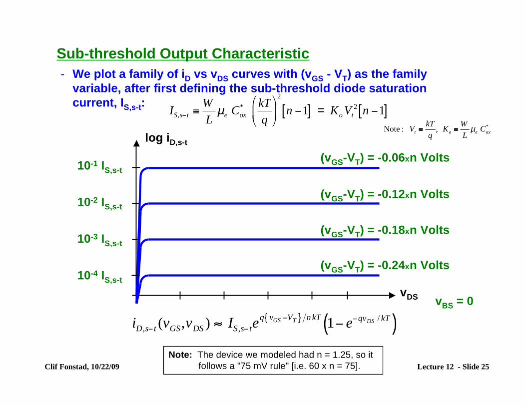
- We plot a family of iD vs vDS curves with (vGS - VT) as the family variable, after first defining the sub-threshold diode saturation current, IS,s-t:
log iD,s-t
(vGS-VT) = -0.06xn Volts 10-1 IS,s-t
(vGS-VT) = -0.12xn Volts 10-2 IS,s-t
(vGS-VT) = -0.18xn Volts 10-3 IS,s-t
(vGS-VT) = -0.24xn Volts 10-4 IS,s-t
vDS vBS = 0
!
Note : Vt"
kT
q, K
o"
W
Lµ
eC
ox
*
!
iD,s" t
(vGS
,vDS
) # IS,s" t
eq v
GS"V
T{ } n kT
1" e"qv
DS/ kT( )
Note: The device we modeled had n = 1.25, so it follows a "75 mV rule" [i.e. 60 x n = 75]. Clif Fonstad, 10/22/09 Lecture 12 - Slide 25
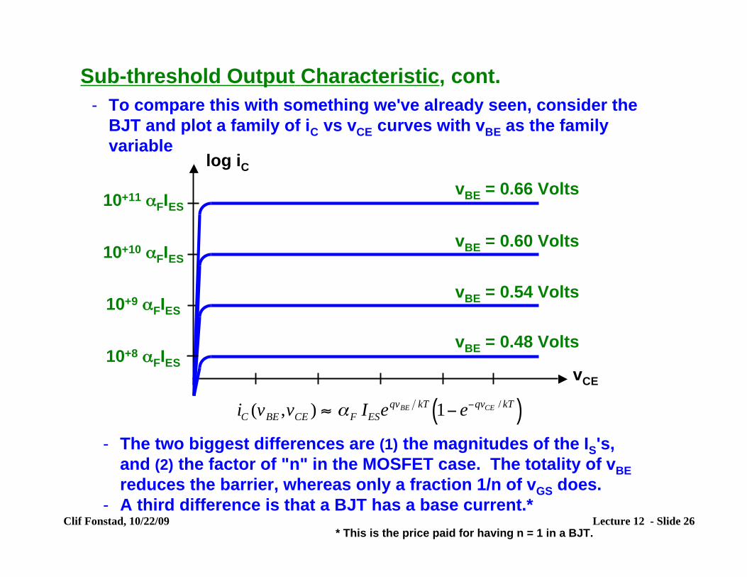
Sub-threshold Output Characteristic, cont. - To compare this with something we've already seen, consider the
BJT and plot a family of iC vs vCE curves with vBE as the family variable
!
iC(v
BE,v
CE) " #
FI
ESe
qvBE
kT1$ e
$qvCE
/ kT( )
log iC
vCE
10+11 αFIES
10+10 αFIES
10+9 αFIES
10+8 αFIES
vBE = 0.66 Volts
vBE = 0.60 Volts
vBE = 0.54 Volts
vBE = 0.48 Volts
- The two biggest differences are (1) the magnitudes of the IS's, and (2) the factor of "n" in the MOSFET case. The totality of vBE reduces the barrier, whereas only a fraction 1/n of vGS does.
- A third difference is that a BJT has a base current.* Clif Fonstad, 10/22/09 Lecture 12 - Slide 26
* This is the price paid for having n = 1 in a BJT.
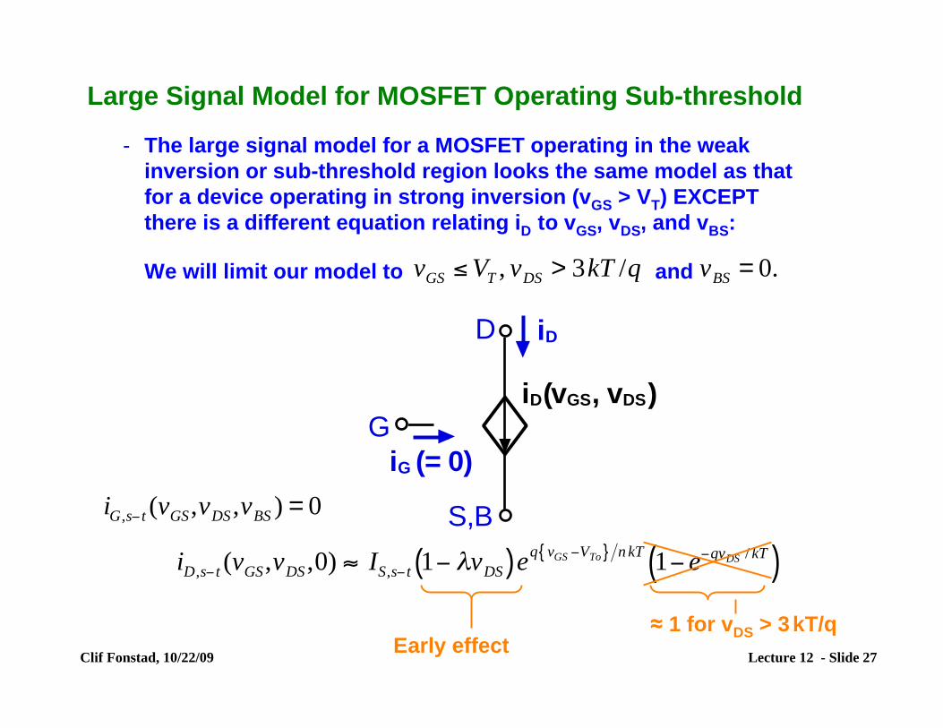
Large Signal Model for MOSFET Operating Sub-threshold
- The large signal model for a MOSFET operating in the weak inversion or sub-threshold region looks the same model as that for a device operating in strong inversion (vGS > VT) EXCEPT there is a different equation relating iD to vGS, vDS, and vBS:
We will limit our model to and
!
vGS"V
T, v
DS> 3kT /q v
BS= 0.
Clif Fonstad, 10/22/09 Lecture 12 - Slide 27
!
iD,s" t
(vGS
,vDS
,0) # IS,s" t
1" $vDS( )e
q vGS"V
To{ } n kT
1" e"qv
DS/ kT( )
!
iG,s" t
(vGS
,vDS
,vBS
) = 0
Early effect ≈ 1 for vDS > 3 kT/q
G
S,B
D
iD(vGS, vDS)
iG (= 0)
iD
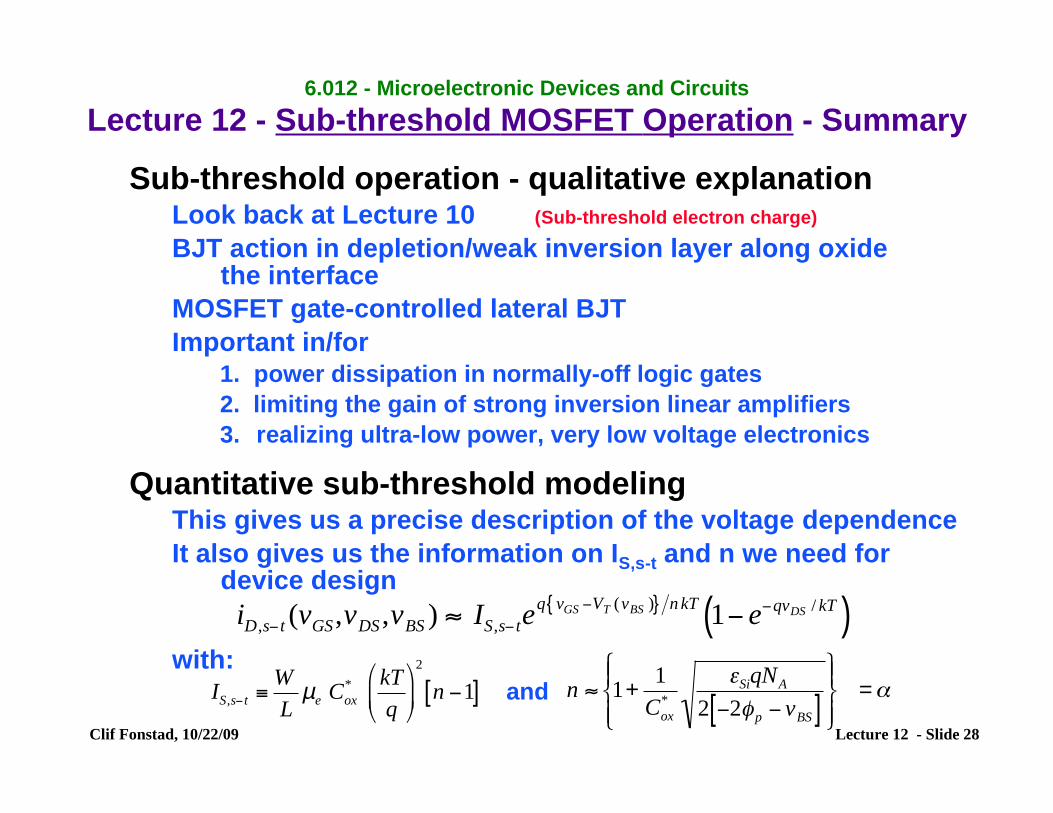
6.012 - Microelectronic Devices and Circuits Lecture 12 - Sub-threshold MOSFET Operation - Summary
Sub-threshold operation - qualitative explanation Look back at Lecture 10 (Sub-threshold electron charge)
BJT action in depletion/weak inversion layer along oxidethe interface
MOSFET gate-controlled lateral BJT Important in/for
1. power dissipation in normally-off logic gates 2. limiting the gain of strong inversion linear amplifiers 3. realizing ultra-low power, very low voltage electronics
Quantitative sub-threshold modeling This gives us a precise description of the voltage dependence It also gives us the information on IS,s-t and n we need for
device design
Clif Fonstad, 10/22/09 Lecture 12 - Slide 28
with:
!
IS,s" t
#W
Lµ
eC
ox
* kT
q
$
% &
'
( )
2
n "1[ ]
!
iD,s" t
(vGS
,vDS
,vBS
) # IS,s" t
eq v
GS"V
T(v
BS){ } n kT
1" e"qv
DS/ kT( )
!
n " 1+1
Cox
*
#SiqN
A
2 $2%p$ v
BS[ ]& ' (
) (
* + (
, ( =-and
MIT OpenCourseWarehttp://ocw.mit.edu
6.012 Microelectronic Devices and Circuits Fall 2009
For information about citing these materials or our Terms of Use, visit: http://ocw.mit.edu/terms.