Schottky Diodes (M-S Contacts)web.it.nctu.edu.tw/~thhou/12-IEEE5561/Chap2-0412.pdf · • N-type...
21
Chapter 2 1 Three MITs of the Day • Band diagrams for ohmic and rectifying Schottky contacts • Similarity to and difference from bipolar junctions on electrostatic and IV characteristics. • Surface Fermi level pinning Reading assignment: Sections 2.4 of Taur & Ning Schottky Diodes (M-S Contacts)
Transcript of Schottky Diodes (M-S Contacts)web.it.nctu.edu.tw/~thhou/12-IEEE5561/Chap2-0412.pdf · • N-type...
Chapter 2 1
Three MITs of the Day
• Band diagrams for ohmic and rectifying Schottky contacts• Similarity to and difference from bipolar junctions on
electrostatic and IV characteristics.• Surface Fermi level pinning
Reading assignment: Sections 2.4 of Taur & Ning
Schottky Diodes (M-S Contacts)
Chapter 2 2
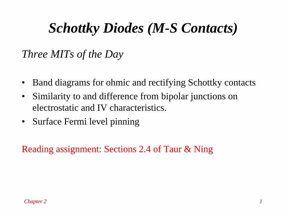
• Ideal MS contacts:– Intimate contacts (no hole or bubble)– No intermixing/diffusion– No surface charge/traps
• If we keep on increasing the p doping of a p+-n diode, the p side will go through Mott transition around 1021cm-3 and can be regarded as a M-S contact
• Work function of metal: energy necessary for electrons to be free electrons in vacuum.
• Metals can be viewed with negative or negligible bandgap(many silicides are metals electrically)
qVbi
EV
E0
EFM
x=Wx=0
EFn
ΦM
ΦB
ΦSχ
EV
E0
EFM
x=0
EFn
ΦM ΦSχ
(1) n-type Si, ΦM >ΦS , Rectifying
(2) n-type Si, ΦM <ΦS, Ohmic
E0
E0
Band Diagrams
Chapter 2 3
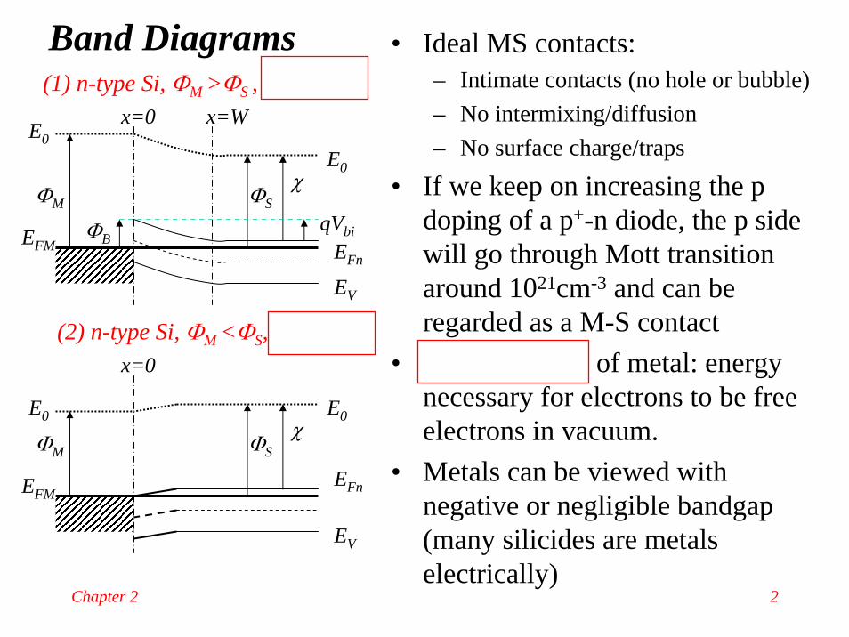
Steady-state IV of a Schottky diode• N-type semiconductors
– ΦM > ΦS: retifying– qVbi= ΦM - ΦS= ΦB - (EC-EF)FB
– ΦM < ΦS: Ohmic
• P-type semiconductors– ΦM < ΦS: retifying– ΦM > ΦS: Ohmic
q(Vbi-VA)
EV
E0
EFM
x=Wx=0
EFn
ΦM
ΦB
ΦSχ
(1) n-type Si, ΦM >ΦS , Rectifying
E0IM→SIS→M
• What is different from the bipolar diodes?
• IV are dominated by carriers having enough kinetic energy to ballistically pass the potential barrier (thermionic emission)
• IM→S remains almost constant for changing VA, since the metal electrons look at the same barrier
• Is→M will change exponentially with VA (with η=1) since the semiconductor electrons look at a barrier height lowered by VA
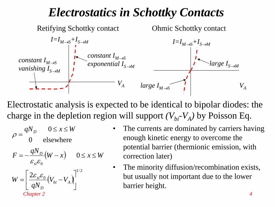
Chapter 2 4
constant IM→Svanishing IS→M
Retifying Schottky contactI=IM→S+IS→M
constant IM→Sexponential IS→M
VA large IM→S
I=IM→S+IS→M
large IS→M
VA
Ohmic Schottky contact
Electrostatic analysis is expected to be identical to bipolar diodes: the charge in the depletion region will support (Vbi-VA) by Poisson Eq.
( )
( )2/1
0
0
2
0
elsewhere00
⎥⎦
⎤⎢⎣
⎡−=
≤≤−−=
≤≤=
AbiD
si
si
D
D
VVqN
W
WxxWqNF
WxqN
εε
εε
ρ
Electrostatics in Schottky Contacts
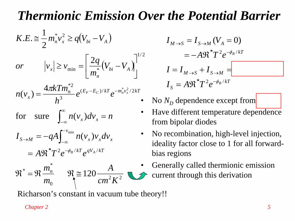
• The currents are dominated by carriers having enough kinetic energy to overcome the potential barrier (thermionic emission, with correction later)
• The minority diffusion/recombination exists, but usually not important due to the lower barrier height.
Chapter 2 5
Thermionic Emission Over the Potential Barrier( )
( )
220
**
//2
2//)(3
2*
2/1
*min
2*
120
)(
)(surefor
4)(
2
21..
min
2*
KcmA
mm
eeTA
dvvvnqAI
ndvvn
eeh
kTmvn
VVm
qvvor
VVqvmEK
n
kTqVkT
v
xxxMS
xx
kTvmkTEEnx
Abin
x
Abixn
AB
xnCF
≅ℜℜ=ℜ
ℜ=
−=
=
=
⎥⎦
⎤⎢⎣
⎡−=≥
−≥≅
−
−
∞−→
∞
∞−
−−
∫∫
φ
π
*
Richarson’s constant in vacuum tube theory!!
( )kT
S
kTqVSMSSM
kTAMSSM
B
A
B
eTAI
eIIIIeTA
VII
/2
/
/2
1
)0(
φ
φ
−
→→
−
→→
ℜ=
−=+=
ℜ−=
==
*
*
• No ND dependence except from ΦB
• Have different temperature dependence from bipolar diodes
• No recombination, high-level injection, ideality factor close to 1 for all forward-bias regions
• Generally called thermionic emission current through this derivation
Chapter 2 6
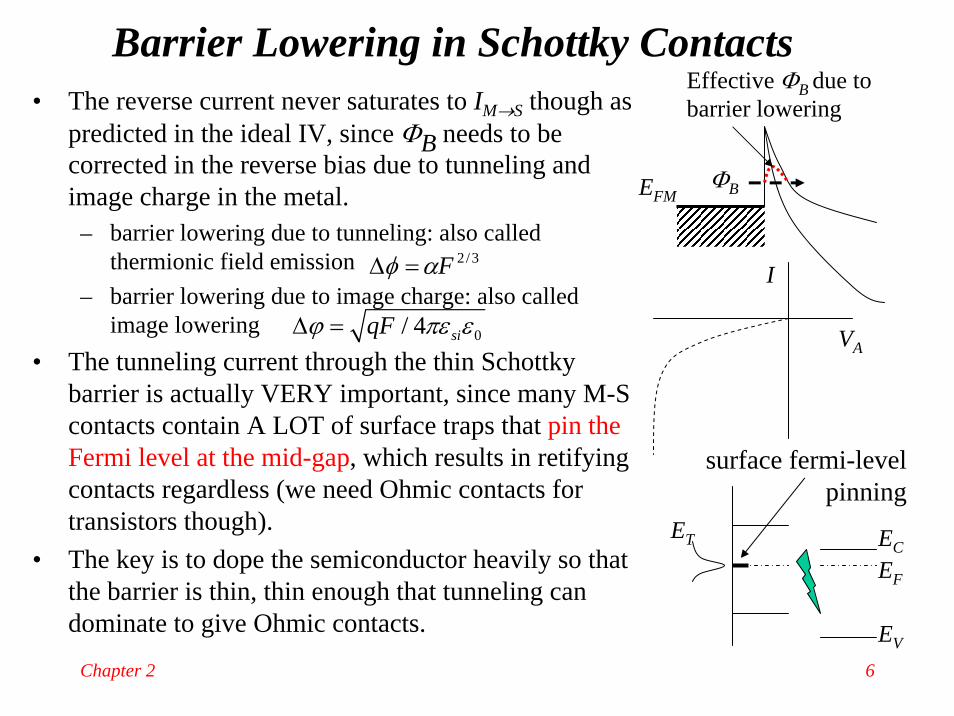
• The reverse current never saturates to IM→S though as predicted in the ideal IV, since ΦB needs to be corrected in the reverse bias due to tunneling and image charge in the metal.– barrier lowering due to tunneling: also called
thermionic field emission– barrier lowering due to image charge: also called
image lowering• The tunneling current through the thin Schottky
barrier is actually VERY important, since many M-S contacts contain A LOT of surface traps that pin the Fermi level at the mid-gap, which results in retifyingcontacts regardless (we need Ohmic contacts for transistors though).
• The key is to dope the semiconductor heavily so that the barrier is thin, thin enough that tunneling can dominate to give Ohmic contacts.
EFMΦB
Effective ΦB due to barrier lowering
VA
I
EF
EC
EV
ET
surface fermi-level pinning
0/ 4 siqFϕ πε εΔ =
3/2Fαφ =Δ
Barrier Lowering in Schottky Contacts
Chapter 2 7
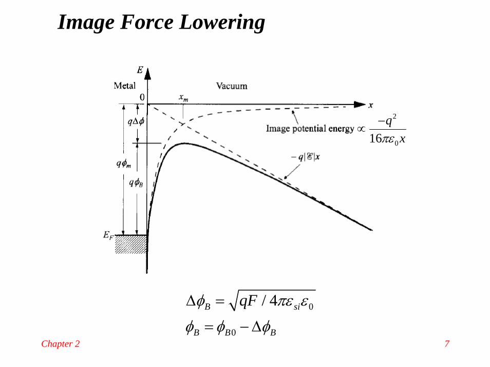
Image Force Lowering
0
0
/ 4B si
B B B
qFφ πε εφ φ φΔ =
= − Δ
2
016q
xπε−
∝
Chapter 2 8
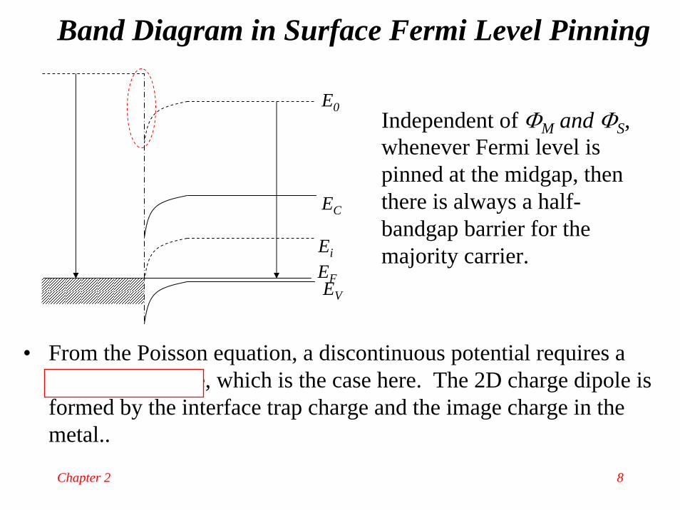
• From the Poisson equation, a discontinuous potential requires a 2D charge dipole, which is the case here. The 2D charge dipole is formed by the interface trap charge and the image charge in the metal..
Band Diagram in Surface Fermi Level Pinning
EC
EV
EF
Ei
E0Independent of ΦM and ΦS, whenever Fermi level is pinned at the midgap, then there is always a half-bandgap barrier for the majority carrier.
Chapter 2 9
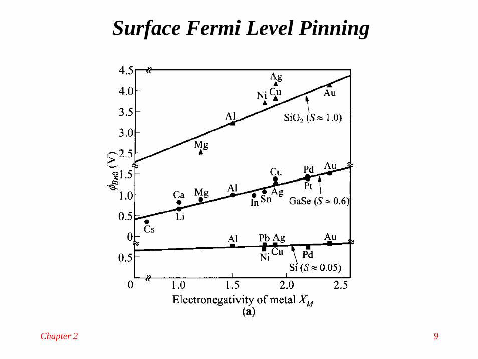
Surface Fermi Level Pinning
Chapter 2 10
• The small-signal behavior of Schottky diodes is similar to the bipolar diode case (required by electrostatics)
• The transient response of the Schottky diodes is much faster than the bipolar diode case, since the minority carrier does not “participate in” (they surely exist, but usually very small) and there is no hold time for diode to go from ON to OFF.
• The bipolar current (diffusion) and the Schottky current (thermionic emission with correction) can actually be unified in one expression, but the algebra is too complex, and the interested reader should visit S. M. Sze’s Physics of Semiconductor Devices (Wiley 1981), presented under the thermionic diffusion theory.
Schottky Diodes vs. Bipolar Diodes
Chapter 2 11
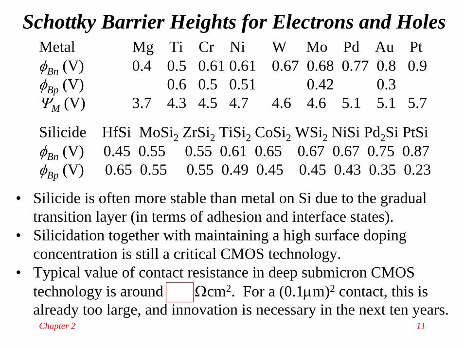
Schottky Barrier Heights for Electrons and HolesMetal Mg Ti Cr Ni W Mo Pd Au PtφBn (V) 0.4 0.5 0.61 0.61 0.67 0.68 0.77 0.8 0.9φBp (V) 0.6 0.5 0.51 0.42 0.3ΨM (V) 3.7 4.3 4.5 4.7 4.6 4.6 5.1 5.1 5.7
Silicide HfSi MoSi2 ZrSi2 TiSi2 CoSi2 WSi2 NiSi Pd2Si PtSiφBn (V) 0.45 0.55 0.55 0.61 0.65 0.67 0.67 0.75 0.87φBp (V) 0.65 0.55 0.55 0.49 0.45 0.45 0.43 0.35 0.23
• Silicide is often more stable than metal on Si due to the gradual transition layer (in terms of adhesion and interface states).
• Silicidation together with maintaining a high surface doping concentration is still a critical CMOS technology.
• Typical value of contact resistance in deep submicron CMOS technology is around 10-7 Ωcm2. For a (0.1μm)2 contact, this is already too large, and innovation is necessary in the next ten years.
Chapter 2 12
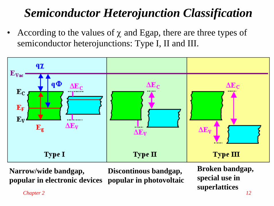
Semiconductor Heterojunction Classification• According to the values of χ and Egap, there are three types of
semiconductor heterojunctions: Type I, II and III.
Narrow/wide bandgap, popular in electronic devices
Discontinous bandgap, popular in photovoltaic
Broken bandgap, special use in superlattices
Chapter 2 13
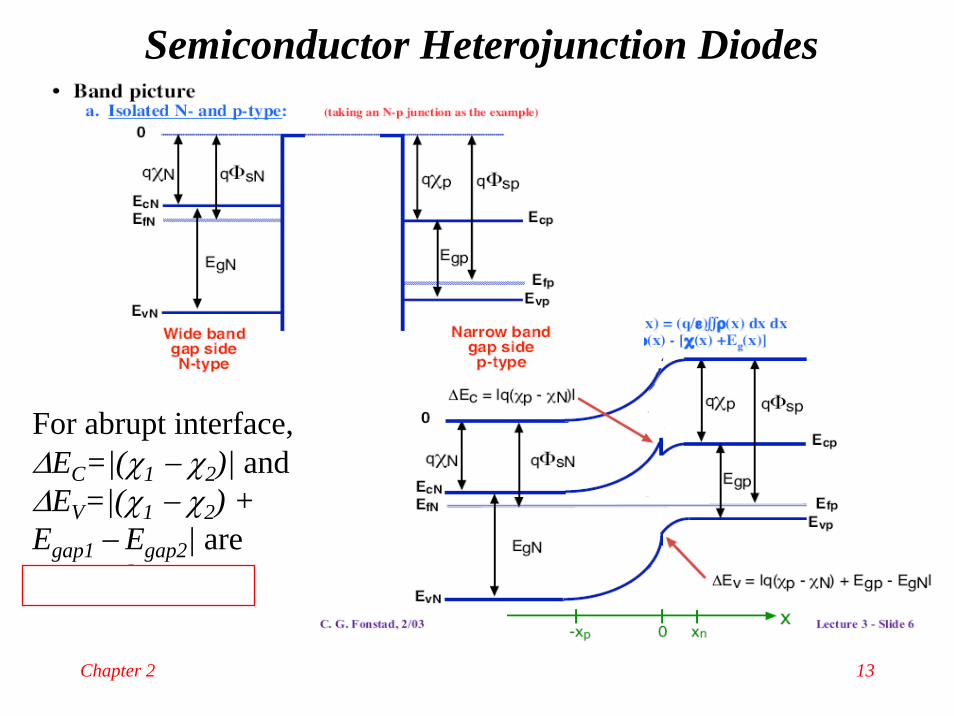
Semiconductor Heterojunction Diodes
For abrupt interface, ΔEC=|(χ1 − χ2)| and ΔEV=|(χ1 − χ2) + Egap1 − Egap2| are material constant
Chapter 2 14
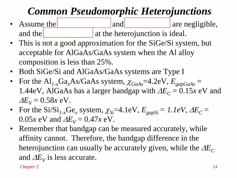
Common Pseudomorphic Heterojunctions• Assume the lattice mismatch and residual stress are negligible,
and the lattice interface at the heterojunction is ideal. • This is not a good approximation for the SiGe/Si system, but
acceptable for AlGaAs/GaAs system when the Al alloy composition is less than 25%.
• Both SiGe/Si and AlGaAs/GaAs systems are Type I • For the Al1-xGaxAs/GaAs system, χGaAs=4.2eV, EgapGaAs =
1.44eV, AlGaAs has a larger bandgap with ΔEC = 0.15x eV and ΔEV = 0.58x eV.
• For the Si/Si1-xGex system, χSi=4.1eV, EgapSi = 1.1eV, ΔEC = 0.05x eV and ΔEV = 0.47x eV.
• Remember that bandgap can be measured accurately, while affinity cannot. Therefore, the bandgap difference in the heterojunction can usually be accurately given, while the ΔECand ΔEV is less accurate.
Chapter 2 15
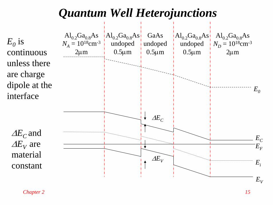
Quantum Well Heterojunctions
Al0.2Ga0.8AsNA = 1018cm-3
2μm
GaAsundoped0.5μm
Al0.2Ga0.8Asundoped0.5μm
Al0.2Ga0.8Asundoped0.5μm
Al0.2Ga0.8AsND = 1018cm-3
2μm
EF
E0
EC
Ei
ΔEC
ΔEV
EV
ΔEC and ΔEV are material constant
E0 is continuous unless there are charge dipole at the interface
Chapter 2 16
Three MITs of the Day
• Relations of semiconductor bandgap and optical properties• Photosensitive regions of diodes: optical generation that
can produce currents• Avalanche operations for photo-amplification
Diode Applications
Chapter 2 17
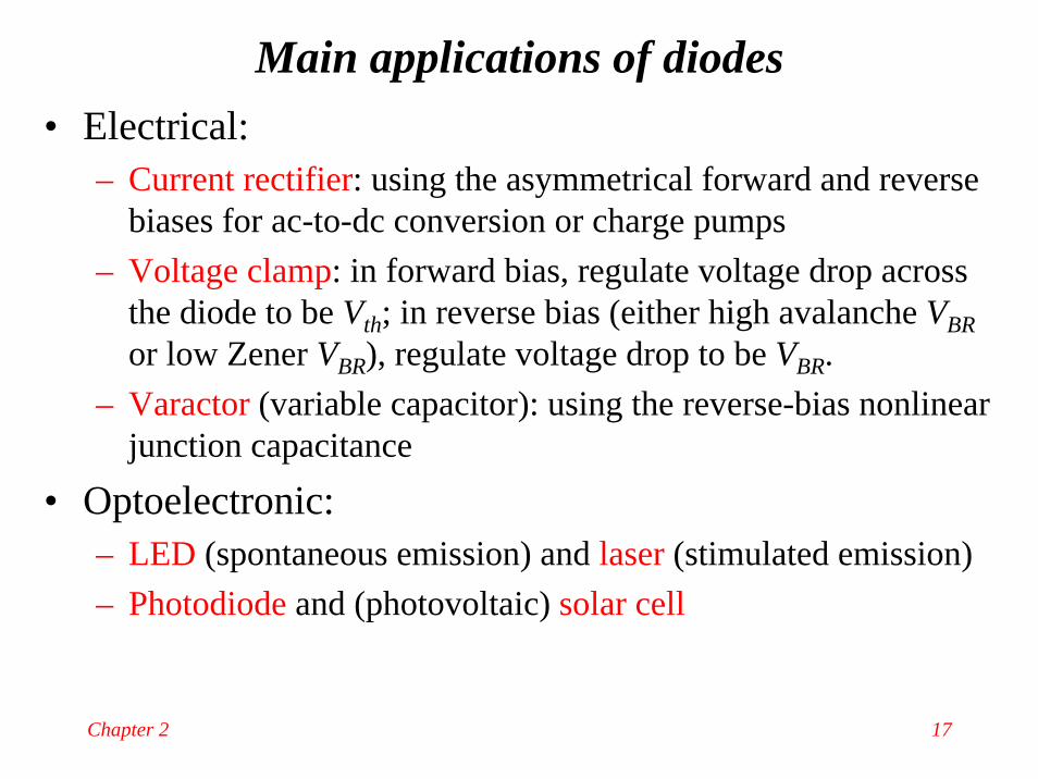
Main applications of diodes• Electrical:
– Current rectifier: using the asymmetrical forward and reverse biases for ac-to-dc conversion or charge pumps
– Voltage clamp: in forward bias, regulate voltage drop across the diode to be Vth; in reverse bias (either high avalanche VBRor low Zener VBR), regulate voltage drop to be VBR.
– Varactor (variable capacitor): using the reverse-bias nonlinear junction capacitance
• Optoelectronic:– LED (spontaneous emission) and laser (stimulated emission)– Photodiode and (photovoltaic) solar cell
Chapter 2 18
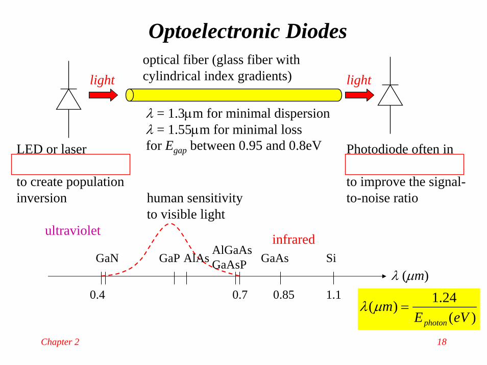
Optoelectronic Diodes
λ = 1.3μm for minimal dispersionλ = 1.55μm for minimal lossfor Egap between 0.95 and 0.8eV
optical fiber (glass fiber with cylindrical index gradients)
LED or laserheavily forward bias to create population inversion
Photodiode often in avalanche breakdown to improve the signal-to-noise ratio
λ (μm)
human sensitivity to visible light
GaN GaP AlAs
ultraviolet
GaAs Si
0.4 0.7 0.85 1.1
infrared
)(24.1)(
eVEm
photon
=μλ
light light
AlGaAsGaAsP
Chapter 2 19
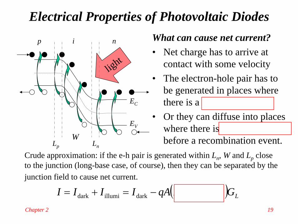
Electrical Properties of Photovoltaic Diodes
light
EC
EV
Crude approximation: if the e-h pair is generated within Ln, W and Lp close to the junction (long-base case, of course), then they can be separated by the junction field to cause net current.
WLnLp
p i n
( ) Lpn GWLLqAIIII ++−=+= darkillumidark
What can cause net current?• Net charge has to arrive at
contact with some velocity• The electron-hole pair has to
be generated in places where there is a separation F.
• Or they can diffuse into places where there is separation Fbefore a recombination event.
Chapter 2 20
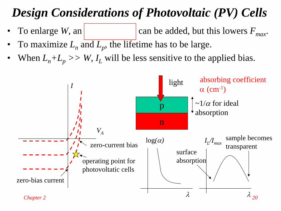
zero-bias current
I
zero-current bias
VA
p
n
light absorbing coefficient α (cm-1)
~1/α for ideal absorption
log(α)
λ
IL/Imax
λ
sample becomes transparent
surface absorption
• To enlarge W, an intrinsic layer can be added, but this lowers Fmax.• To maximize Ln and Lp, the lifetime has to be large.• When Ln+Lp >> W, IL will be less sensitive to the applied bias.
operating point for photovoltatic cells
Design Considerations of Photovoltaic (PV) Cells
Chapter 2 21
• Photodetectors:– Preferably operating in the avalanche region (sometime called avalanche
diodes) to improve sensitivity, since one photon can generate multiple electron/hole pairs from multiplication.
• Solar cells:– Most sunlight is visible to infrared (before the ozone layer is gone)– Si and GaAs can be used, but how to grow on a large area?? (thin-film)– Satellite applications (cost and integration not a problem): GaAs or other
direct bandgap materials (about 25-35% efficiency)– Commercial applications: a-Si and c-Si (about 10-15% efficiency)
• LEDs (light-emitting diodes):– Large direct bandgap material is needed for visible light (1.77eV < Egap <
3.10eV) for (0.4μm < λ < 0.7μm).– Need to have both electrons and holes at the same location with small τ.– New directions: GaN and organic LED.
Three Basic Types of “Photo” Diodes