
S Unidirectional Bidirectional S SMA - Home ... 2018 DocID17869 Rev 4 1/13 This is information on a...
13
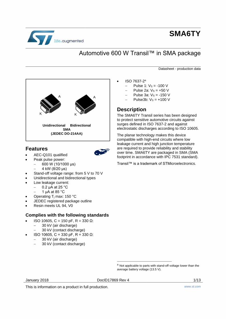
January 2018 DocID17869 Rev 4 1/13 This is information on a product in full production. www.st.com SMA6TY Automotive 600 W Transil™ in SMA package Datasheet - production data Features AEC-Q101 qualified Peak pulse power: 600 W (10/1000 μs) 4 kW (8/20 μs) Stand-off voltage range: from 5 V to 70 V Unidirectional and bidirectional types Low leakage current: 0.2 μA at 25 °C 1 μA at 85 °C Operating Tj max: 150 °C JEDEC registered package outline Resin meets UL 94, V0 Complies with the following standards ISO 10605, C = 150 pF, R = 330 Ω: 30 kV (air discharge) 30 kV (contact discharge) ISO 10605, C = 330 pF, R = 330 Ω: 30 kV (air discharge) 30 kV (contact discharge) ISO 7637-2 a Pulse 1: VS = -100 V Pulse 2a: VS = +50 V Pulse 3a: VS = -150 V Pulse3b: VS = +100 V Description The SMA6TY Transil series has been designed to protect sensitive automotive circuits against surges defined in ISO 7637-2 and against electrostatic discharges according to ISO 10605. The planar technology makes this device compatible with high-end circuits where low leakage current and high junction temperature are required to provide reliability and stability over time. SMA6TY are packaged in SMA (SMA footprint in accordance with IPC 7531 standard). Transil™ is a trademark of STMicroelectronics. a Not applicable to parts with stand-off voltage lower than the average battery voltage (13.5 V). K A Unidirectional Bidirectional SMA (JEDEC DO-214AA) K A
Transcript of S Unidirectional Bidirectional S SMA - Home ... 2018 DocID17869 Rev 4 1/13 This is information on a...
January 2018 DocID17869 Rev 4 1/13
This is information on a product in full production. www.st.com
SMA6TY
Automotive 600 W Transil™ in SMA package
Datasheet - production data
Features AEC-Q101 qualified
Peak pulse power:
600 W (10/1000 μs)
4 kW (8/20 μs)
Stand-off voltage range: from 5 V to 70 V
Unidirectional and bidirectional types
Low leakage current:
0.2 μA at 25 °C
1 μA at 85 °C
Operating Tj max: 150 °C
JEDEC registered package outline
Resin meets UL 94, V0
Complies with the following standards
ISO 10605, C = 150 pF, R = 330 Ω:
30 kV (air discharge)
30 kV (contact discharge)
ISO 10605, C = 330 pF, R = 330 Ω:
30 kV (air discharge)
30 kV (contact discharge)
ISO 7637-2a
Pulse 1: VS = -100 V
Pulse 2a: VS = +50 V
Pulse 3a: VS = -150 V
Pulse3b: VS = +100 V
Description The SMA6TY Transil series has been designed to protect sensitive automotive circuits against surges defined in ISO 7637-2 and against electrostatic discharges according to ISO 10605.
The planar technology makes this device compatible with high-end circuits where low leakage current and high junction temperature are required to provide reliability and stability over time. SMA6TY are packaged in SMA (SMA footprint in accordance with IPC 7531 standard).
Transil™ is a trademark of STMicroelectronics.
a Not applicable to parts with stand-off voltage lower than the
average battery voltage (13.5 V).
K
A
Unidirectional Bidirectional
SMA
(JEDEC DO-214AA)
K
A
Characteristics SMA6TY
2/13 DocID17869 Rev 4
1 Characteristics Table 1: Absolute maximum ratings (Tamb = 25 °C)
Symbol Parameter
Value Unit
VPP Peak pulse voltage
ISO10605 (C = 330 pF, R = 330 Ω):
Contact discharge
Air discharge
ISO10605 / IEC 61000-4-2
(C = 150 pF, R = 330 Ω)
Contact discharge
Air discharge
30
30
30
30
kV
PPP Peak pulse power dissipation 10/1000 µs, Tj initial = Tamb 600 W
Tj Operating junction temperature range -40 to +150 °C
TSTG Storage temperature range -65 to +150 °C
TL Maximum lead temperature for soldering during 10 s 260 °C
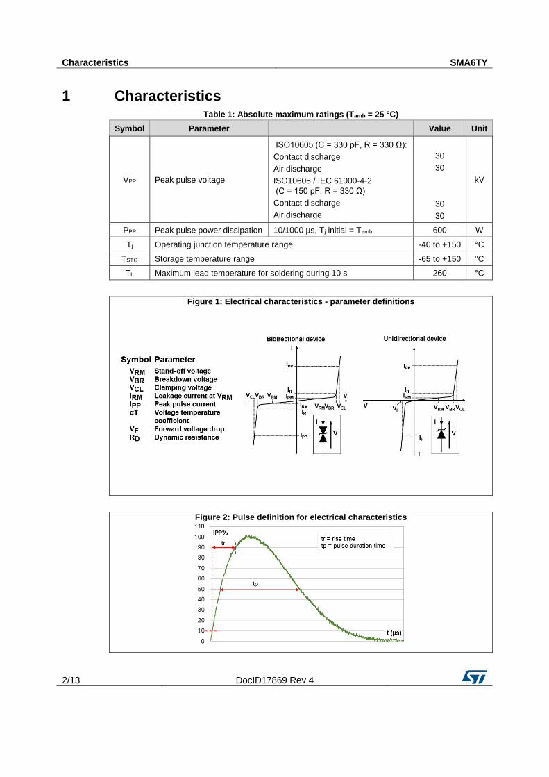
Figure 1: Electrical characteristics - parameter definitions
Figure 2: Pulse definition for electrical characteristics
SMA6TY Characteristics
DocID17869 Rev 4 3/13
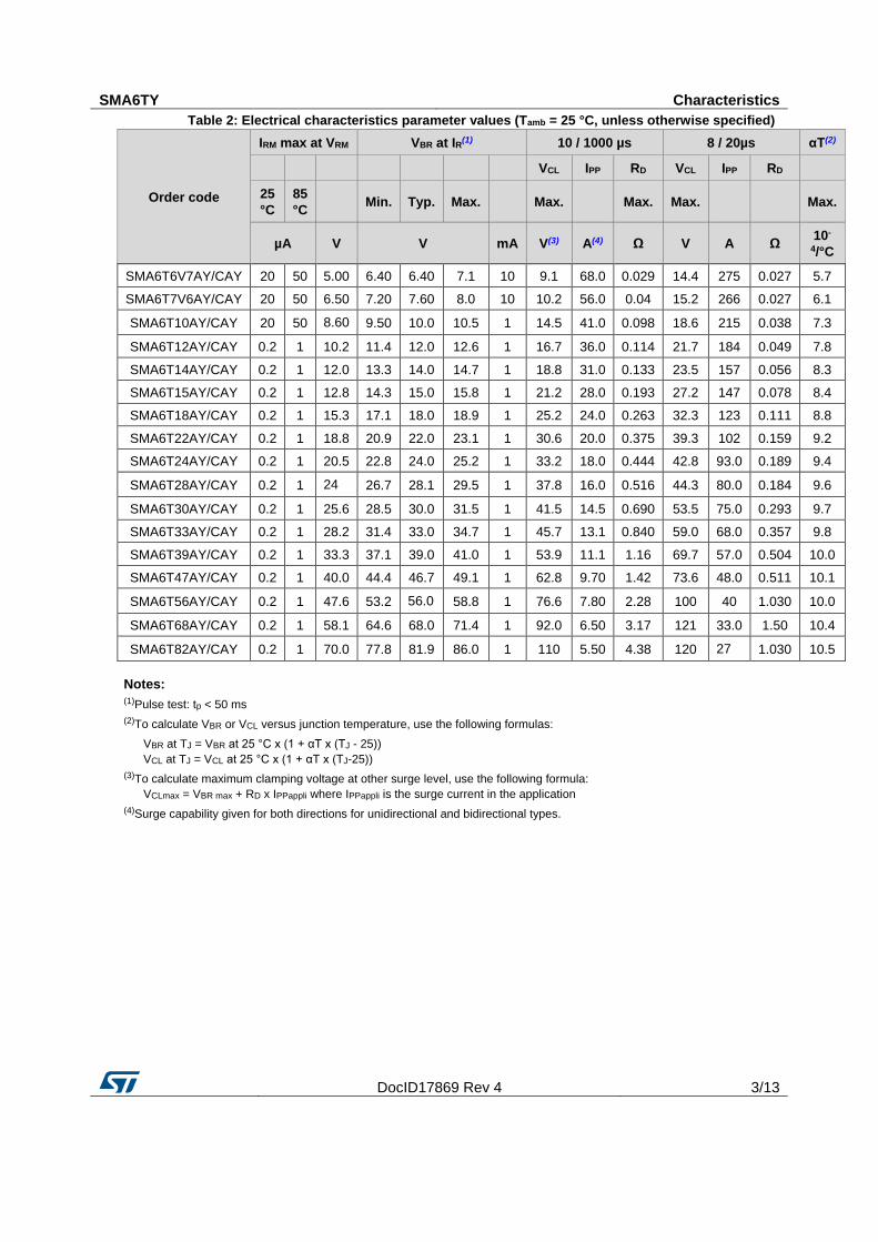
Table 2: Electrical characteristics parameter values (Tamb = 25 °C, unless otherwise specified)
Order code
IRM max at VRM VBR at IR(1) 10 / 1000 µs 8 / 20µs αT(2)
VCL IPP RD VCL IPP RD
25
°C
85
°C Min. Typ. Max.
Max.
Max. Max.
Max.
µA V V mA V(3) A(4) Ω V A Ω 10-
4/°C
SMA6T6V7AY/CAY 20 50 5.00 6.40 6.40 7.1 10 9.1 68.0 0.029 14.4 275 0.027 5.7
SMA6T7V6AY/CAY 20 50 6.50 7.20 7.60 8.0 10 10.2 56.0 0.04 15.2 266 0.027 6.1
SMA6T10AY/CAY 20 50 8.60 9.50 10.0 10.5 1 14.5 41.0 0.098 18.6 215 0.038 7.3
SMA6T12AY/CAY 0.2 1 10.2 11.4 12.0 12.6 1 16.7 36.0 0.114 21.7 184 0.049 7.8
SMA6T14AY/CAY 0.2 1 12.0 13.3 14.0 14.7 1 18.8 31.0 0.133 23.5 157 0.056 8.3
SMA6T15AY/CAY 0.2 1 12.8 14.3 15.0 15.8 1 21.2 28.0 0.193 27.2 147 0.078 8.4
SMA6T18AY/CAY 0.2 1 15.3 17.1 18.0 18.9 1 25.2 24.0 0.263 32.3 123 0.111 8.8
SMA6T22AY/CAY 0.2 1 18.8 20.9 22.0 23.1 1 30.6 20.0 0.375 39.3 102 0.159 9.2
SMA6T24AY/CAY 0.2 1 20.5 22.8 24.0 25.2 1 33.2 18.0 0.444 42.8 93.0 0.189 9.4
SMA6T28AY/CAY 0.2 1 24 26.7 28.1 29.5 1 37.8 16.0 0.516 44.3 80.0 0.184 9.6
SMA6T30AY/CAY 0.2 1 25.6 28.5 30.0 31.5 1 41.5 14.5 0.690 53.5 75.0 0.293 9.7
SMA6T33AY/CAY 0.2 1 28.2 31.4 33.0 34.7 1 45.7 13.1 0.840 59.0 68.0 0.357 9.8
SMA6T39AY/CAY 0.2 1 33.3 37.1 39.0 41.0 1 53.9 11.1 1.16 69.7 57.0 0.504 10.0
SMA6T47AY/CAY 0.2 1 40.0 44.4 46.7 49.1 1 62.8 9.70 1.42 73.6 48.0 0.511 10.1
SMA6T56AY/CAY 0.2 1 47.6 53.2 56.0 58.8 1 76.6 7.80 2.28 100 40 1.030 10.0
SMA6T68AY/CAY 0.2 1 58.1 64.6 68.0 71.4 1 92.0 6.50 3.17 121 33.0 1.50 10.4
SMA6T82AY/CAY 0.2 1 70.0 77.8 81.9 86.0 1 110 5.50 4.38 120 27 1.030 10.5
Notes: (1)Pulse test: tp < 50 ms (2)To calculate VBR or VCL versus junction temperature, use the following formulas:
VBR at TJ = VBR at 25 °C x (1 + αT x (TJ - 25))
VCL at TJ = VCL at 25 °C x (1 + αT x (TJ-25)) (3)To calculate maximum clamping voltage at other surge level, use the following formula:
VCLmax = VBR max + RD x IPPappli where IPPappli is the surge current in the application (4)Surge capability given for both directions for unidirectional and bidirectional types.
Characteristics SMA6TY
4/13 DocID17869 Rev 4
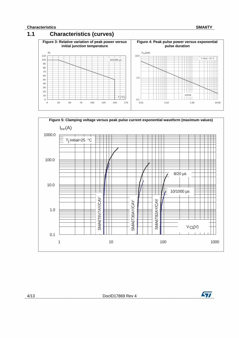
1.1 Characteristics (curves)
Figure 3: Relative variation of peak power versus initial junction temperature
Figure 4: Peak pulse power versus exponential pulse duration
Figure 5: Clamping voltage versus peak pulse current exponential waveform (maximum values)
0
10
20
30
40
50
60
70
80
90
100
110
0 25 50 75 100 125 150 175
%
T (°C)j
10/1000 µs
PPP(kW)
0.1
1.0
10.0
0.01 0.10 1.00 10.00
Tj initial = 25 °C
tP(ms)
0.1
1.0
10.0
100.0
1000.0
1 10 100 1000
IPP(A)
10/1000 µs
Tj initial=25 °C
8/20 µs
VCL(V)VCL(V)
SM
A6T
6V
7A
Y/C
AY
SM
A6T
30A
Y/C
AY
SM
A6T
82A
Y/C
AY
SMA6TY Characteristics
DocID17869 Rev 4 5/13
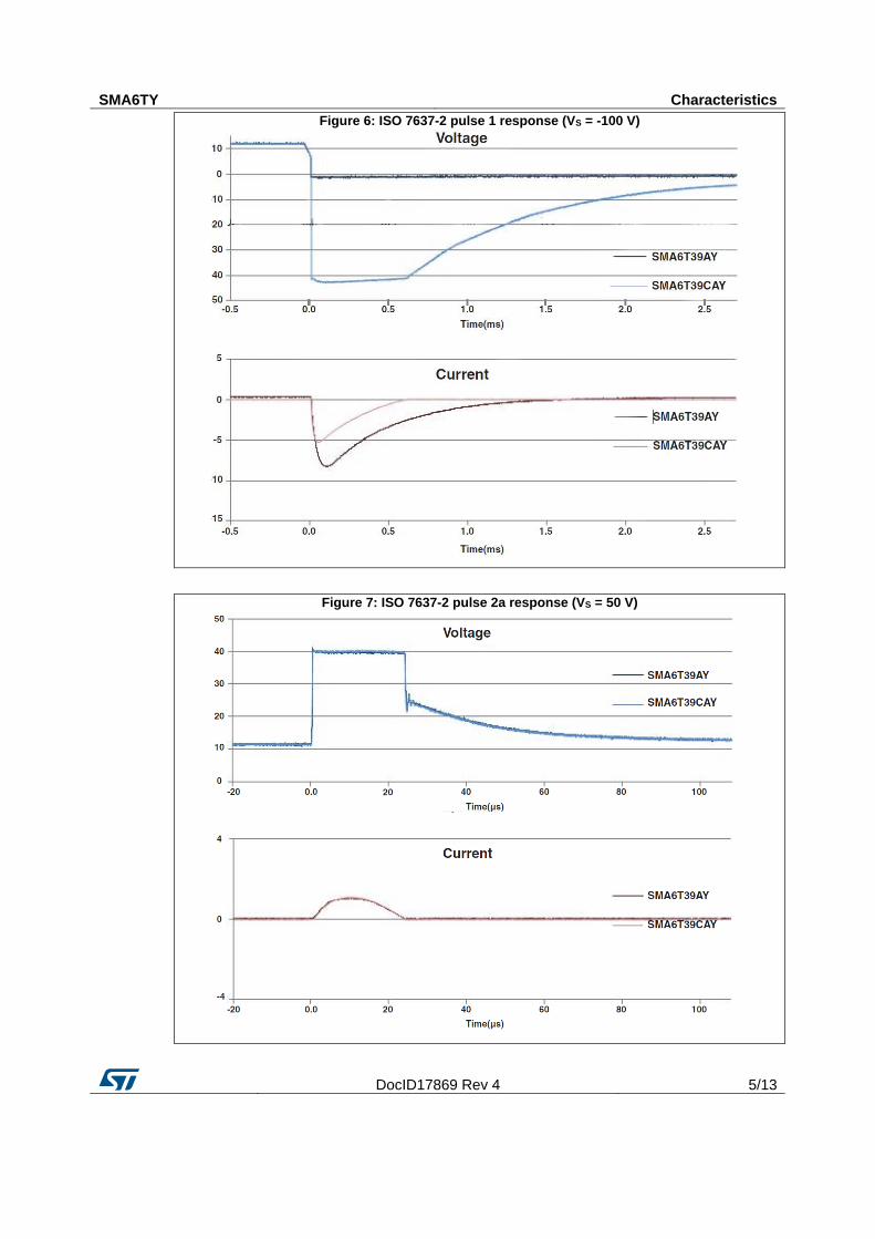
Figure 6: ISO 7637-2 pulse 1 response (VS = -100 V)
Figure 7: ISO 7637-2 pulse 2a response (VS = 50 V)
Characteristics SMA6TY
6/13 DocID17869 Rev 4
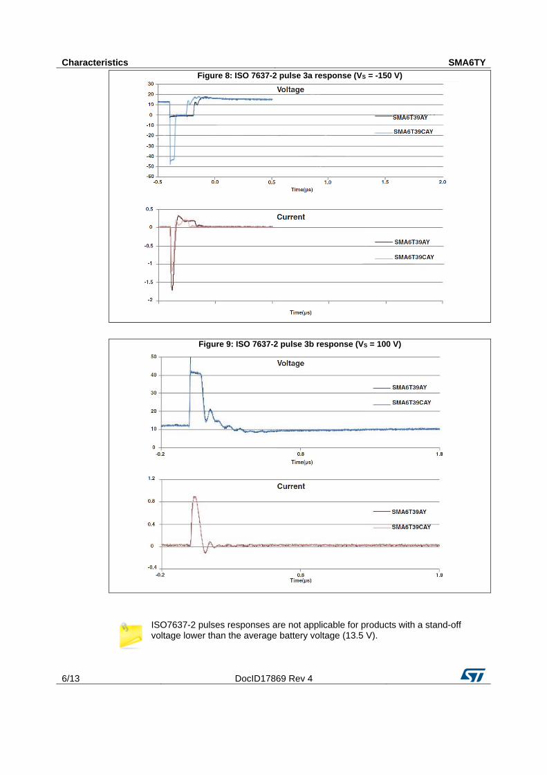
Figure 8: ISO 7637-2 pulse 3a response (VS = -150 V)
Figure 9: ISO 7637-2 pulse 3b response (VS = 100 V)
ISO7637-2 pulses responses are not applicable for products with a stand-off voltage lower than the average battery voltage (13.5 V).
SMA6TY Characteristics
DocID17869 Rev 4 7/13
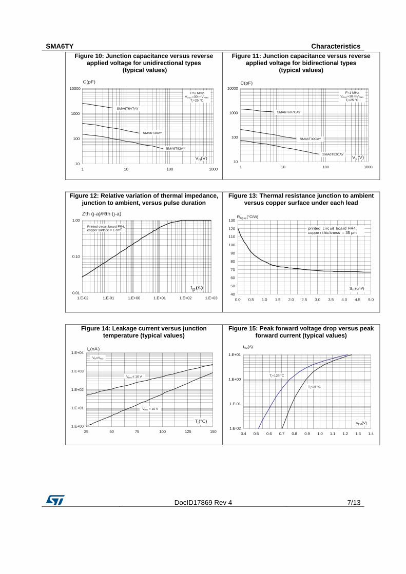
Figure 10: Junction capacitance versus reverse applied voltage for unidirectional types
(typical values)
Figure 11: Junction capacitance versus reverse applied voltage for bidirectional types
(typical values)
Figure 12: Relative variation of thermal impedance, junction to ambient, versus pulse duration
Figure 13: Thermal resistance junction to ambient versus copper surface under each lead
Figure 14: Leakage current versus junction temperature (typical values)
Figure 15: Peak forward voltage drop versus peak forward current (typical values)
C(pF)
10
100
1000
10000
1 10 100 1000
F=1 MHz
VOSC=30 mVRMS
Tj=25 °C
SMA6T6V7AY
SMA6T30AY
SMA6T82AY
V (V)R
C(pF)
10
100
1000
10000
1 10 100 1000
F=1 MHzVOSC=30 mVRMS
Tj=25 °C
SMA6T6V7CAY
SMA6T30CAY
SMA6T82CAYV (V)R
Zth (j-a)/Rth (j-a)
0.01
0.10
1.00
1.E-02 1.E-01 1.E+00 1.E+01 1.E+02 1.E+03
stp
Printed circuit board FR4,copper surface = 1 cm2
Rth(j-a)(°C/W)
40
50
60
70
80
90
100
110
120
130
0.0 0.5 1.0 1.5 2.0 2.5 3.0 3.5 4.0 4.5 5.0
printed circuit board FR4,coppe r thickness = 35 µm
SCu(cm²)
I (nA)R
1.E+00
1.E+01
1.E+02
1.E+03
1.E+04
25 50 75 100 125 150
VR=VRM
VRM > 10 V
VRM ≤ 10 V
T (°C)j
IFM(A)
1.E-02
1.E-01
1.E+00
1.E+01
0.4 0.5 0.6 0.7 0.8 0.9 1.0 1.1 1.2 1.3 1.4
Tj=25 °C
Tj=125 °C
VFM(V)
Package information SMA6TY
8/13 DocID17869 Rev 4
2 Package information In order to meet environmental requirements, ST offers these devices in different grades of ECOPACK® packages, depending on their level of environmental compliance. ECOPACK® specifications, grade definitions and product status are available at: www.st.com. ECOPACK® is an ST trademark.
Case: JEDEC DO214-AA molded plastic over planar junction
Terminals: solder plated, solderable per MIL-STD-750, method 2026
Polarity: for unidirectional types the band indicates cathode
Flammability: epoxy is rated UL94V-0
RoHS package
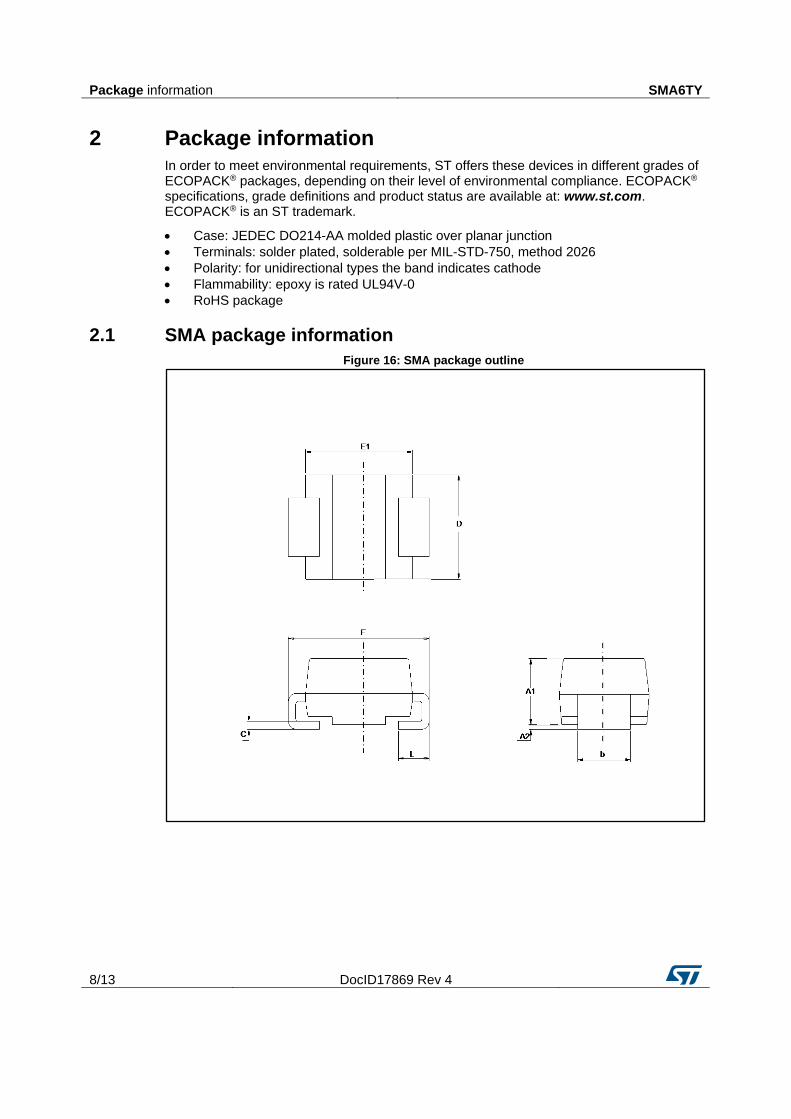
2.1 SMA package information
Figure 16: SMA package outline
SMA6TY Package information
DocID17869 Rev 4 9/13
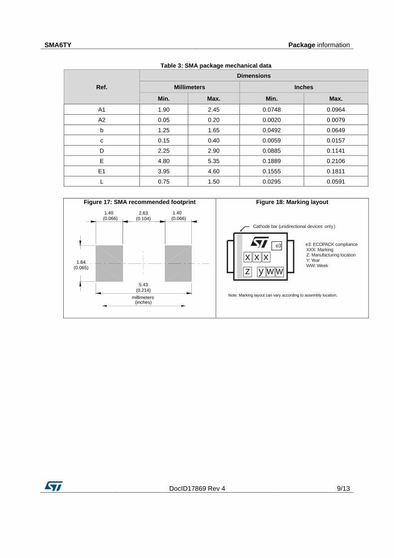
Table 3: SMA package mechanical data
Ref.
Dimensions
Millimeters Inches
Min. Max. Min. Max.
A1 1.90 2.45 0.0748 0.0964
A2 0.05 0.20 0.0020 0.0079
b 1.25 1.65 0.0492 0.0649
c 0.15 0.40 0.0059 0.0157
D 2.25 2.90 0.0885 0.1141
E 4.80 5.35 0.1889 0.2106
E1 3.95 4.60 0.1555 0.1811
L 0.75 1.50 0.0295 0.0591
Figure 17: SMA recommended footprint
Figure 18: Marking layout
millimeters(inches)
1.40
(0.066)
1.40
(0.066)2.63
(0.104)
5.43
(0.214)
1.64
(0.065)y w w
e3
z
x x x
e3: ECOPACK complianceXXX: MarkingZ: Manufacturing locationY: YearWW: Week
Cathode bar (unidirectional devices only )
Note: Marking layout can vary according to assembly location.
Ordering information SMA6TY
10/13 DocID17869 Rev 4
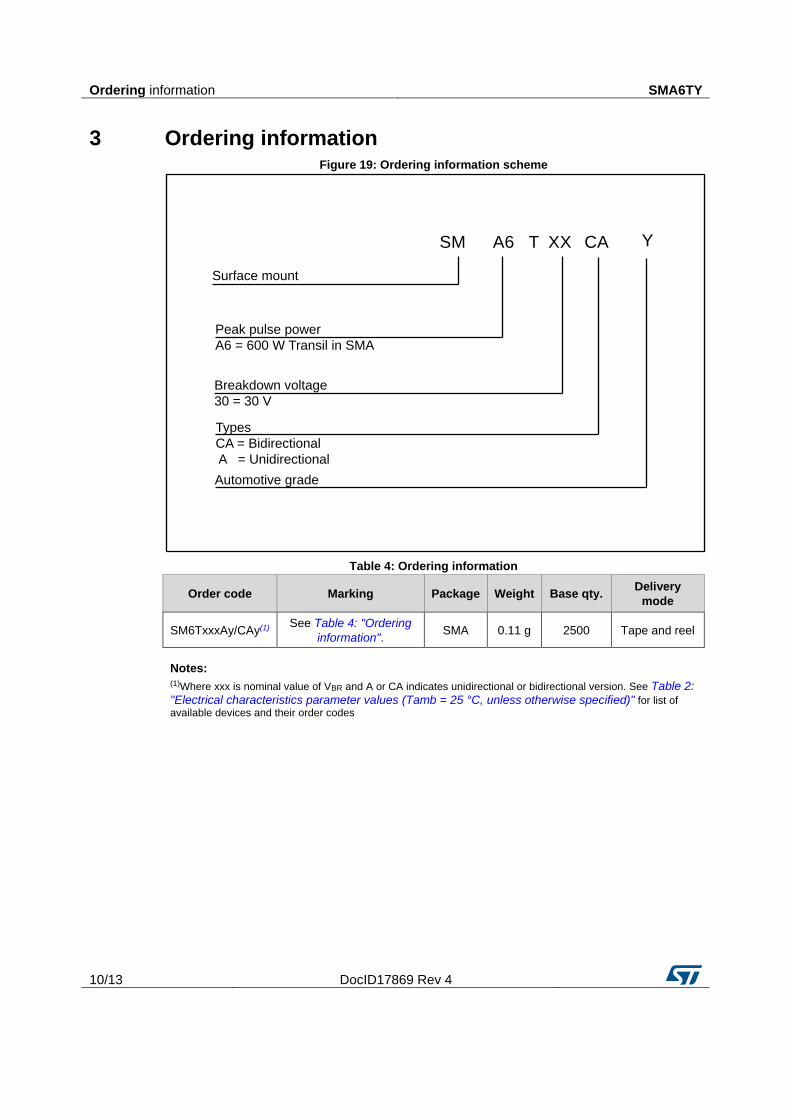
3 Ordering information Figure 19: Ordering information scheme
Table 4: Ordering information
Order code Marking Package Weight Base qty. Delivery
mode
SM6TxxxAy/CAy(1) See Table 4: "Ordering
information". SMA 0.11 g 2500 Tape and reel
Notes: (1)Where xxx is nominal value of VBR and A or CA indicates unidirectional or bidirectional version. See Table 2: "Electrical characteristics parameter values (Tamb = 25 °C, unless otherwise specified)" for list of available devices and their order codes
SM A6 T XX CA
Surface mount
Peak pulse power
A6 = 600 W Transil in SMA
Breakdown voltage
30 = 30 V
Types
CA = Bidirectional
A = Unidirectional
Automotive grade
Y
SMA6TY Ordering information
DocID17869 Rev 4 11/13
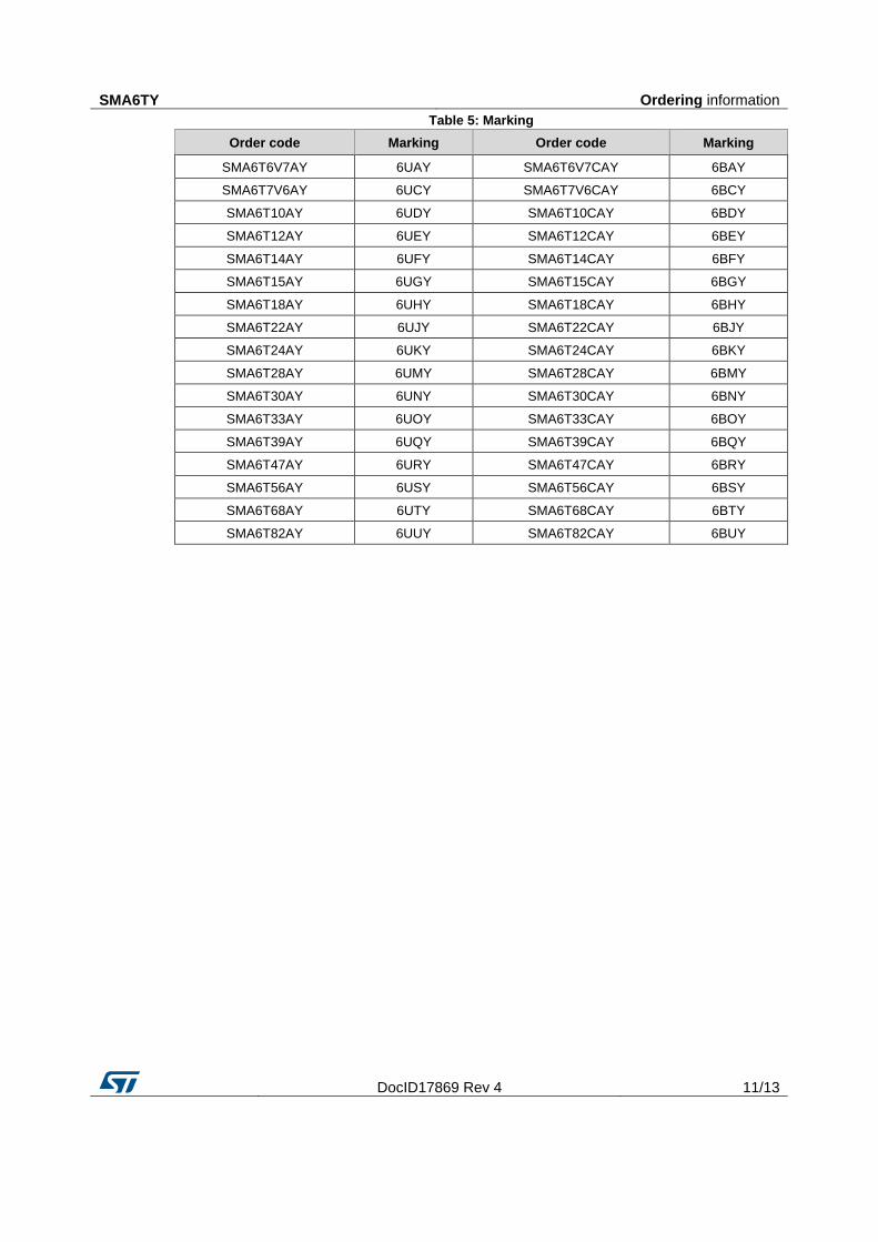
Table 5: Marking
Order code Marking Order code Marking
SMA6T6V7AY 6UAY SMA6T6V7CAY 6BAY
SMA6T7V6AY 6UCY SMA6T7V6CAY 6BCY
SMA6T10AY 6UDY SMA6T10CAY 6BDY
SMA6T12AY 6UEY SMA6T12CAY 6BEY
SMA6T14AY 6UFY SMA6T14CAY 6BFY
SMA6T15AY 6UGY SMA6T15CAY 6BGY
SMA6T18AY 6UHY SMA6T18CAY 6BHY
SMA6T22AY 6UJY SMA6T22CAY 6BJY
SMA6T24AY 6UKY SMA6T24CAY 6BKY
SMA6T28AY 6UMY SMA6T28CAY 6BMY
SMA6T30AY 6UNY SMA6T30CAY 6BNY
SMA6T33AY 6UOY SMA6T33CAY 6BOY
SMA6T39AY 6UQY SMA6T39CAY 6BQY
SMA6T47AY 6URY SMA6T47CAY 6BRY
SMA6T56AY 6USY SMA6T56CAY 6BSY
SMA6T68AY 6UTY SMA6T68CAY 6BTY
SMA6T82AY 6UUY SMA6T82CAY 6BUY
Revision history SMA6TY
12/13 DocID17869 Rev 4
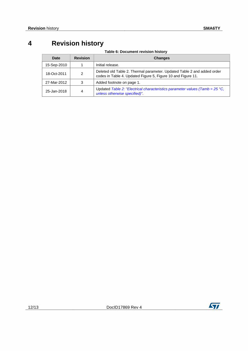
4 Revision history Table 6: Document revision history
Date Revision Changes
15-Sep-2010 1 Initial release.
18-Oct-2011 2 Deleted old Table 2. Thermal parameter. Updated Table 2 and added order
codes in Table 4. Updated Figure 5, Figure 10 and Figure 11.
27-Mar-2012 3 Added footnote on page 1.
25-Jan-2018 4 Updated Table 2: "Electrical characteristics parameter values (Tamb = 25 °C,
unless otherwise specified)".
SMA6TY
DocID17869 Rev 4 13/13
IMPORTANT NOTICE – PLEASE READ CAREFULLY
STMicroelectronics NV and its subsidiaries (“ST”) reserve the right to make changes, corrections, enhancements, modifications , and improvements to ST products and/or to this document at any time without notice. Purchasers should obtain the latest relevant information on ST products before placing orders. ST products are sold pursuant to ST’s terms and conditions of sale in place at the time of order acknowledgement.
Purchasers are solely responsible for the choice, selection, and use of ST products and ST assumes no liability for application assistance or the design of Purchasers’ products.
No license, express or implied, to any intellectual property right is granted by ST herein.
Resale of ST products with provisions different from the information set forth herein shall void any warranty granted by ST for such product.
ST and the ST logo are trademarks of ST. All other product or service names are the property of their respective owners.
Information in this document supersedes and replaces information previously supplied in any prior versions of this document.
© 2018 STMicroelectronics – All rights reserved


![Cyanobacteria [Exetwotion, SMA 1 Depok]](https://static.fdocument.org/doc/165x107/558812e1d8b42a42658b4579/cyanobacteria-exetwotion-sma-1-depok.jpg)