RP111x Series - hu.mouser.com
46
RP111x Series Good Transient Response Low Voltage 500mA LDO NO.EA-241-190523 1 OUTLINE The RP111x Series are CMOS-based LDO regulators featuring 500mA output current. The input voltage is as low as 1.4V and the output voltage can be set from 0.7V. Due to a built-in 0.46Ω (at VOUT=2.8V) on-resistor, RP111x can provide a low dropout voltage. RP111x also features an excellent line transient response, ripple rejection at 75dB, and low noise. The output voltage accuracy is as high as ±0.8% and the temperature drift coefficient of output voltage is low at ±30ppm/°C. The accuracy of the output voltage of RP111x includes the temperature characteristics and the load transient response has been improved. The typ. and max value of under/overshoot for various output current are shown in the typical characteristics in the datasheet, therefore the accuracy of the output voltage estimation will be easy on the actual operating cases. In addition to a fold-back protection circuit built into conventional regulators, RP111x contains a thermal shutdown circuit and an inrush current limit circuit. SOT-23-5 and SOT-89-5 packages, a 1.2mm square DFN1212-6 package are available. FEATURES • Supply Current ...................................................... Typ. 80µA • Standby Current .................................................... Typ. 0.1µA • Dropout Voltage .................................................... Typ. 0.23V (IOUT=500mA, VOUT=2.5V) • Ripple Rejection .................................................... Typ. 75dB (f=1kHz) Typ. 70dB (f=10kHz) • Output Voltage Accuracy....................................... ±0.8% (VOUT ≥1.8V) • Output Voltage Temperature Coefficient ............... Typ. ±30ppm/°C (VOUT ≥1.8V) • Line Regulation ..................................................... Typ. 0.02%/V • Packages .............................................................. DFN1212-6, SOT-23-5, SOT-89-5, • Input Voltage Range ............................................. 1.4V to 5.25V • Output Voltage Range........................................... 0.7V to 3.6V (0.1V steps) (For other voltages, please refer to MARK INFORMATIONS.) • Built-in Foldback Protection Circuit ....................... Typ. 50mA (Current at short mode) • Thermal Shutdown Temperature........................... 165°C • Inrush Current Limit .............................................. Typ.400mA (for 180µs after start-up) • Ceramic capacitors are recommended to be used with this IC ..... 1.0µF or more APPLICATIONS • Power source for portable communication equipment. • Power source for electrical appliances such as cameras, VCRs and camcorders. • Power source for battery-powered equipments. • Power source for electrical home appliances.
Transcript of RP111x Series - hu.mouser.com

RP111x Series
Good Transient Response Low Voltage 500mA LDO
NO.EA-241-190523
1
OUTLINE The RP111x Series are CMOS-based LDO regulators featuring 500mA output current. The input voltage is as
low as 1.4V and the output voltage can be set from 0.7V. Due to a built-in 0.46Ω (at VOUT=2.8V) on-resistor, RP111x can provide a low dropout voltage. RP111x also features an excellent line transient response, ripple rejection at 75dB, and low noise. The output voltage accuracy is as high as ±0.8% and the temperature drift coefficient of output voltage is low at ±30ppm/°C. The accuracy of the output voltage of RP111x includes the temperature characteristics and the load transient response has been improved. The typ. and max value of under/overshoot for various output current are shown in the typical characteristics in the datasheet, therefore the accuracy of the output voltage estimation will be easy on the actual operating cases.
In addition to a fold-back protection circuit built into conventional regulators, RP111x contains a thermal shutdown circuit and an inrush current limit circuit. SOT-23-5 and SOT-89-5 packages, a 1.2mm square DFN1212-6 package are available. FEATURES
• Supply Current ...................................................... Typ. 80µA • Standby Current .................................................... Typ. 0.1µA • Dropout Voltage .................................................... Typ. 0.23V (IOUT=500mA, VOUT=2.5V) • Ripple Rejection .................................................... Typ. 75dB (f=1kHz)
Typ. 70dB (f=10kHz) • Output Voltage Accuracy ....................................... ±0.8% (VOUT ≥1.8V) • Output Voltage Temperature Coefficient ............... Typ. ±30ppm/°C (VOUT ≥1.8V) • Line Regulation ..................................................... Typ. 0.02%/V • Packages .............................................................. DFN1212-6, SOT-23-5, SOT-89-5, • Input Voltage Range ............................................. 1.4V to 5.25V • Output Voltage Range ........................................... 0.7V to 3.6V (0.1V steps) (For other voltages, please refer to MARK INFORMATIONS.) • Built-in Foldback Protection Circuit ....................... Typ. 50mA (Current at short mode) • Thermal Shutdown Temperature ........................... 165°C • Inrush Current Limit .............................................. Typ.400mA (for 180µs after start-up) • Ceramic capacitors are recommended to be used with this IC ..... 1.0µF or more
APPLICATIONS
• Power source for portable communication equipment. • Power source for electrical appliances such as cameras, VCRs and camcorders. • Power source for battery-powered equipments. • Power source for electrical home appliances.
RP111x NO.EA-241-190523
2
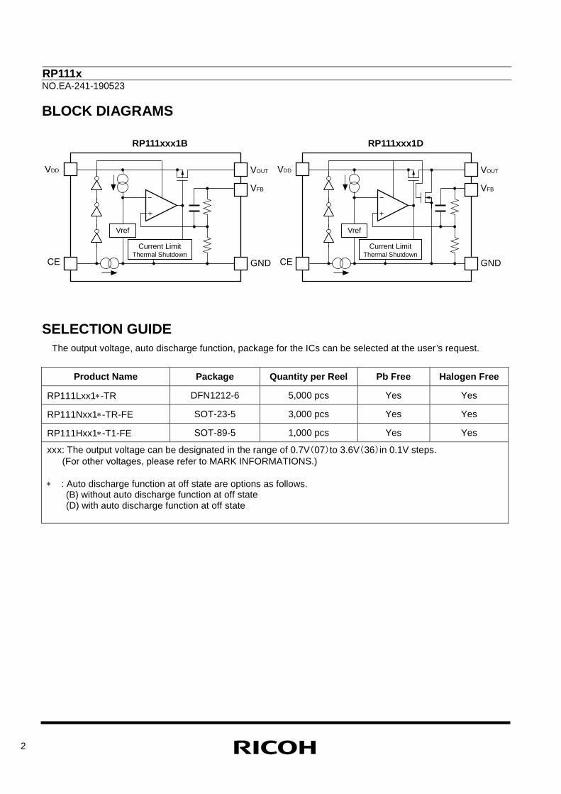
BLOCK DIAGRAMS RP111xxx1B RP111xxx1D VDD
GND
VOUT
CE
Vref
Current Limit Thermal Shutdown
VFB
VDD
GND
VOUT
CE
Vref
Current Limit Thermal Shutdown
VFB
SELECTION GUIDE
The output voltage, auto discharge function, package for the ICs can be selected at the user’s request.
Product Name Package Quantity per Reel Pb Free Halogen Free
RP111Lxx1∗-TR DFN1212-6 5,000 pcs Yes Yes
RP111Nxx1∗-TR-FE SOT-23-5 3,000 pcs Yes Yes
RP111Hxx1∗-T1-FE SOT-89-5 1,000 pcs Yes Yes
xx x: The output voltage can be designated in the range of 0.7V(07)to 3.6V(36)in 0.1V steps. (For other voltages, please refer to MARK INFORMATIONS.) ∗ : Auto discharge function at off state are options as follows. (B) without auto discharge function at off state (D) with auto discharge function at off state
RP111x NO.EA-241-190523
3
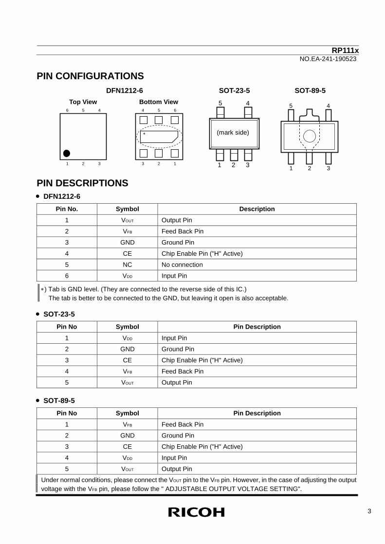
PIN CONFIGURATIONS DFN1212-6 SOT-23-5 SOT-89-5
Top View 6 5 4
1 2 3
Bottom View 4 5 6
3 2 1
∗
1 2 3
4 5
(mark side)
1 3
5 4
2
PIN DESCRIPTIONS • DFN1212-6
Pin No. Symbol Description 1 VOUT Output Pin
2 VFB Feed Back Pin
3 GND Ground Pin
4 CE Chip Enable Pin ("H" Active)
5 NC No connection
6 VDD Input Pin
∗) Tab is GND level. (They are connected to the reverse side of this IC.) The tab is better to be connected to the GND, but leaving it open is also acceptable.
• SOT-23-5
Pin No Symbol Pin Description 1 VDD Input Pin
2 GND Ground Pin
3 CE Chip Enable Pin ("H" Active)
4 VFB Feed Back Pin
5 VOUT Output Pin • SOT-89-5
Pin No Symbol Pin Description 1 VFB Feed Back Pin
2 GND Ground Pin
3 CE Chip Enable Pin ("H" Active)
4 VDD Input Pin
5 VOUT Output Pin
Under normal conditions, please connect the VOUT pin to the VFB pin. However, in the case of adjusting the output voltage with the VFB pin, please follow the " ADJUSTABLE OUTPUT VOLTAGE SETTING".
RP111x NO.EA-241-190523
4
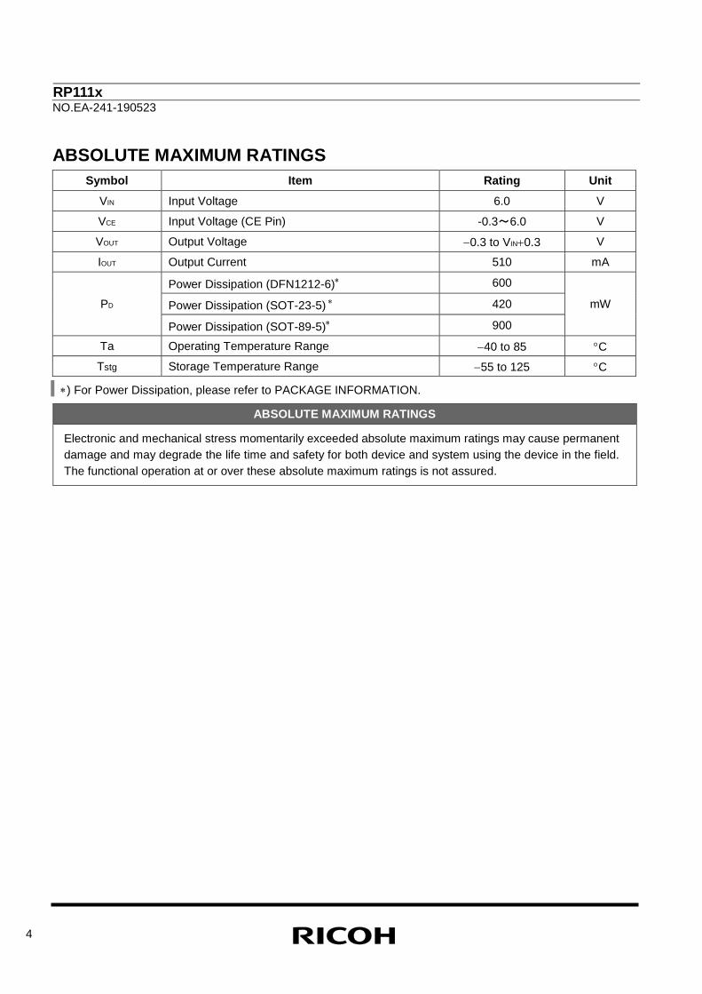
ABSOLUTE MAXIMUM RATINGS Symbol Item Rating Unit
VIN Input Voltage 6.0 V
VCE Input Voltage (CE Pin) -0.3~6.0 V
VOUT Output Voltage −0.3 to VIN+0.3 V
IOUT Output Current 510 mA
PD Power Dissipation (DFN1212-6)∗ 600
mW Power Dissipation (SOT-23-5) ∗ 420
Power Dissipation (SOT-89-5)∗ 900
Ta Operating Temperature Range −40 to 85 °C Tstg Storage Temperature Range −55 to 125 °C
∗) For Power Dissipation, please refer to PACKAGE INFORMATION.
ABSOLUTE MAXIMUM RATINGS
Electronic and mechanical stress momentarily exceeded absolute maximum ratings may cause permanent damage and may degrade the life time and safety for both device and system using the device in the field. The functional operation at or over these absolute maximum ratings is not assured.
RP111x NO.EA-241-190523
5
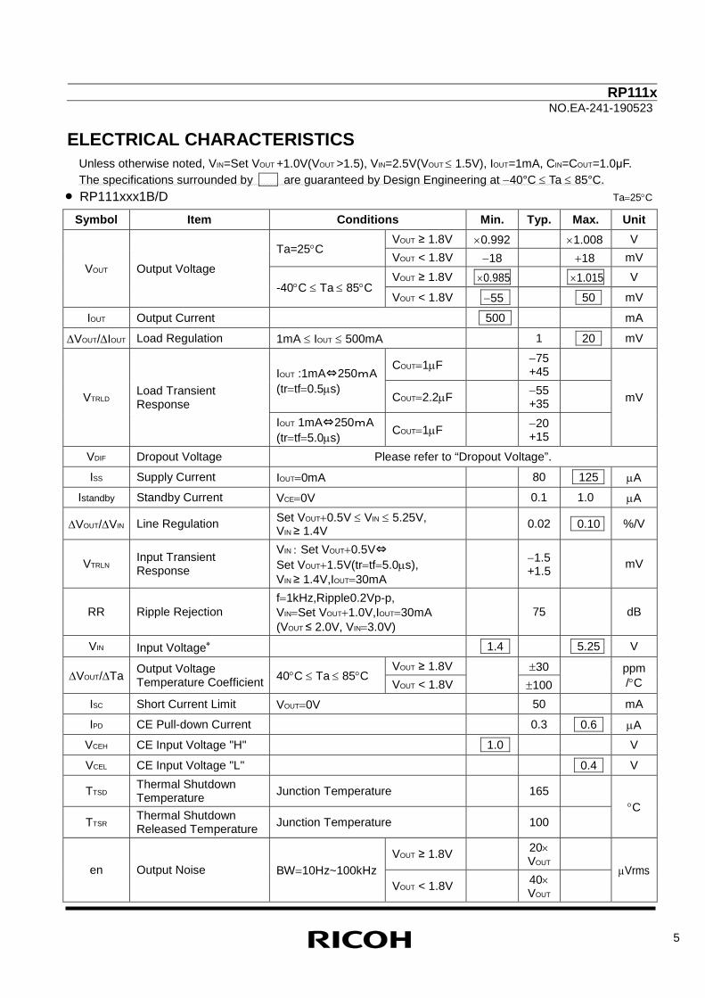
ELECTRICAL CHARACTERISTICS Unless otherwise noted, VIN=Set VOUT +1.0V(VOUT >1.5), VIN=2.5V(VOUT ≤ 1.5V), IOUT=1mA, CIN=COUT=1.0μF. The specifications surrounded by are guaranteed by Design Engineering at −40°C ≤ Ta ≤ 85°C.
• RP111xxx1B/D Ta=25°C
Symbol Item Conditions Min. Typ. Max. Unit
VOUT Output Voltage Ta=25°C
VOUT ≥ 1.8V ×0.992 ×1.008 V VOUT < 1.8V −18 +18 mV
-40°C ≤ Ta ≤ 85°C VOUT ≥ 1.8V ×0.985 ×1.015 V
VOUT < 1.8V −55 50 mV
IOUT Output Current 500 mA
∆VOUT/∆IOUT Load Regulation 1mA ≤ IOUT ≤ 500mA 1 20 mV
VTRLD Load Transient Response
IOUT :1mA⇔250mA (tr=tf=0.5µs)
COUT=1µF −75 +45
mV COUT=2.2µF −55 +35
IOUT 1mA⇔250mA (tr=tf=5.0µs) COUT=1µF −20
+15 VDIF Dropout Voltage Please refer to “Dropout Voltage”.
ISS Supply Current IOUT=0mA 80 125 µA Istandby Standby Current VCE=0V 0.1 1.0 µA
∆VOUT/∆VIN Line Regulation Set VOUT+0.5V ≤ VIN ≤ 5.25V, VIN ≥ 1.4V 0.02 0.10 %/V
VTRLN Input Transient Response
VIN : Set VOUT+0.5V⇔ Set VOUT+1.5V(tr=tf=5.0µs), VIN ≥ 1.4V,IOUT=30mA
−1.5 +1.5 mV
RR Ripple Rejection f=1kHz,Ripple0.2Vp-p, VIN=Set VOUT+1.0V,IOUT=30mA (VOUT ≤ 2.0V, VIN=3.0V)
75 dB
VIN Input Voltage∗ 1.4 5.25 V
∆VOUT/∆Ta Output Voltage Temperature Coefficient 40°C ≤ Ta ≤ 85°C
VOUT ≥ 1.8V ±30 ppm /°C VOUT < 1.8V ±100
ISC Short Current Limit VOUT=0V 50 mA
IPD CE Pull-down Current 0.3 0.6 µA VCEH CE Input Voltage "H" 1.0 V
VCEL CE Input Voltage "L" 0.4 V
TTSD Thermal Shutdown Temperature Junction Temperature 165
°C TTSR Thermal Shutdown
Released Temperature Junction Temperature 100
en Output Noise BW=10Hz~100kHz VOUT ≥ 1.8V 20×
VOUT µVrms
VOUT < 1.8V 40× VOUT
RP111x NO.EA-241-190523
6
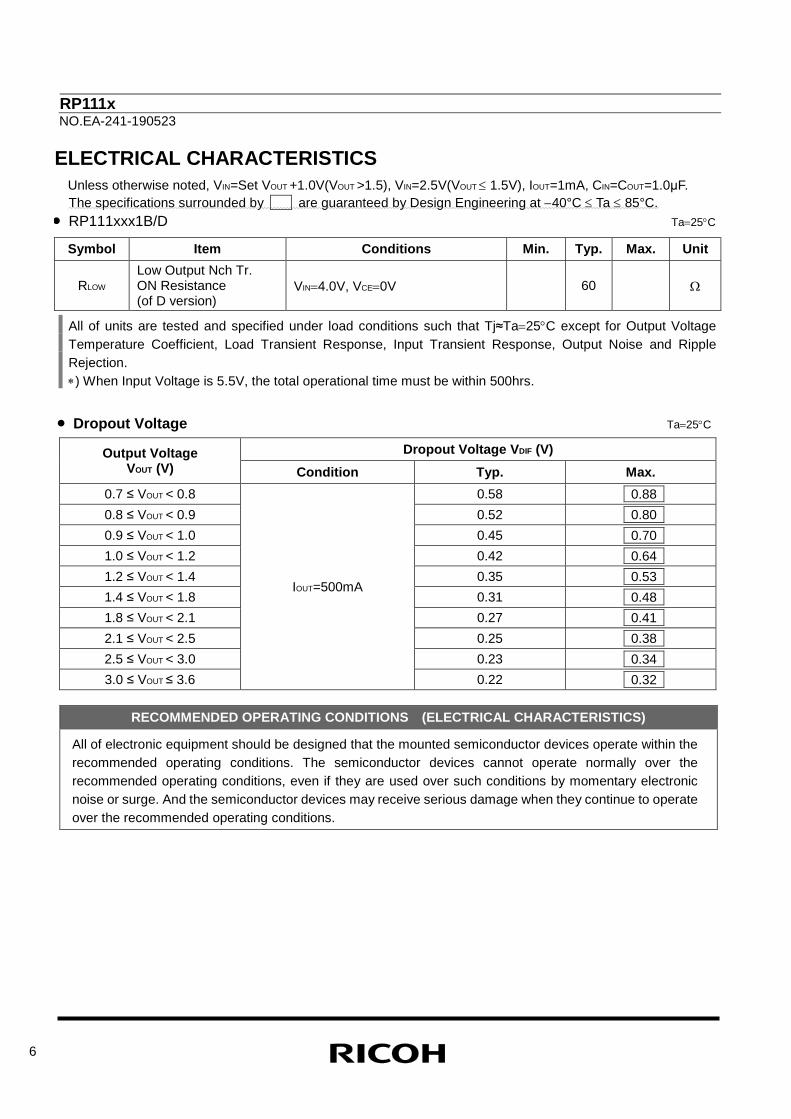
ELECTRICAL CHARACTERISTICS Unless otherwise noted, VIN=Set VOUT +1.0V(VOUT >1.5), VIN=2.5V(VOUT ≤ 1.5V), IOUT=1mA, CIN=COUT=1.0μF. The specifications surrounded by are guaranteed by Design Engineering at −40°C ≤ Ta ≤ 85°C.
• RP111xxx1B/D Ta=25°C
Symbol Item Conditions Min. Typ. Max. Unit
RLOW Low Output Nch Tr. ON Resistance (of D version)
VIN=4.0V, VCE=0V 60 Ω
All of units are tested and specified under load conditions such that Tj≈Ta=25°C except for Output Voltage Temperature Coefficient, Load Transient Response, Input Transient Response, Output Noise and Ripple Rejection. ∗) When Input Voltage is 5.5V, the total operational time must be within 500hrs.
• Dropout Voltage Ta=25°C
Output Voltage VOUT (V)
Dropout Voltage VDIF (V) Condition Typ. Max.
0.7 ≤ VOUT < 0.8
IOUT=500mA
0.58 0.88 0.8 ≤ VOUT < 0.9 0.52 0.80 0.9 ≤ VOUT < 1.0 0.45 0.70 1.0 ≤ VOUT < 1.2 0.42 0.64 1.2 ≤ VOUT < 1.4 0.35 0.53 1.4 ≤ VOUT < 1.8 0.31 0.48 1.8 ≤ VOUT < 2.1 0.27 0.41 2.1 ≤ VOUT < 2.5 0.25 0.38 2.5 ≤ VOUT < 3.0 0.23 0.34 3.0 ≤ VOUT ≤ 3.6 0.22 0.32
RECOMMENDED OPERATING CONDITIONS (ELECTRICAL CHARACTERISTICS)
All of electronic equipment should be designed that the mounted semiconductor devices operate within the recommended operating conditions. The semiconductor devices cannot operate normally over the recommended operating conditions, even if they are used over such conditions by momentary electronic noise or surge. And the semiconductor devices may receive serious damage when they continue to operate over the recommended operating conditions.

RP111x NO.EA-241-190523
7
TYPICAL APPLICATIONS
VOUT
C1 RP111x series
VDD VOUT
GND
C2
CE
VFB
External Parts Example: C1, C2: Ceramic Capacitor 1.0µF, Murata, GRM155B31A105KE15
Under normal conditions, please connect the VOUT pin to the VFB pin. However, in the case of adjusting the output voltage with the VFB pin, please follow the " ADJUSTABLE OUTPUT VOLTAGE SETTING".
TECHNICAL NOTES
Phase Compensation In these ICs, phase compensation is made for securing stable operation even if the load current is varied. For
this purpose, use a 1.0µF or more capacitor C2. In case of using a tantalum capacitor, the output may be unstable due to inappropriate ESR. Therefore, the full
range of operating conditions for the capacitor in the application should be considered.
PCB Layout Make VDD and GND lines sufficient. If their impedance is high, noise pickup or unstable operation may result.
Connect a capacitor C1 with a capacitance value as much as 1.0µF or more between VDD and GND pin, and as close as possible to the pins.
Set external components, especially the output capacitor C2, as close as possible to the ICs, and make wiring as short as possible.
RP111x NO.EA-241-190523
8
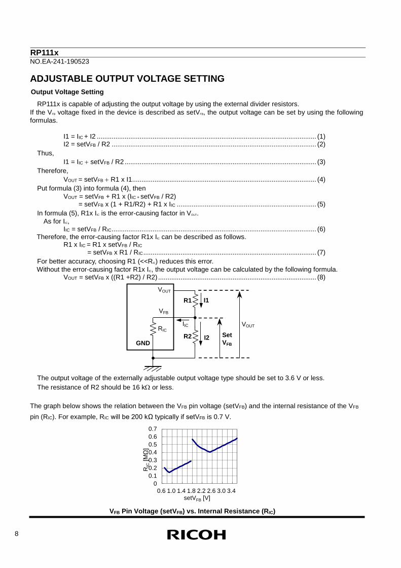
ADJUSTABLE OUTPUT VOLTAGE SETTING Output Voltage Setting
RP111x is capable of adjusting the output voltage by using the external divider resistors. If the VFB voltage fixed in the device is described as setVFB, the output voltage can be set by using the following formulas.
I1 = IIC + I2 ...................................................................................................................... (1) I2 = setVFB / R2 .............................................................................................................. (2)
Thus, I1 = IIC + setVFB / R2 ....................................................................................................... (3)
Therefore, VOUT = setVFB + R1 x I1................................................................................................... (4)
Put formula (3) into formula (4), then VOUT = setVFB + R1 x (IIC + setVFB / R2)
= setVFB x (1 + R1/R2) + R1 x IIC ........................................................................... (5) In formula (5), R1x IIC is the error-causing factor in VOUT. As for IIC,
IIC = setVFB / RIC .............................................................................................................. (6) Therefore, the error-causing factor R1x IIC can be described as follows.
R1 x IIC = R1 x setVFB / RIC= setVFB x R1 / RIC ............................................................................................. (7)
For better accuracy, choosing R1 (<<RIC) reduces this error. Without the error-causing factor R1x IIC, the output voltage can be calculated by the following formula.
VOUT = setVFB x ((R1 +R2) / R2) ..................................................................................... (8)
GND
VOUT
VFB
RIC R2
IIC
I1
I2
R1
Set VFB
VOUT
The output voltage of the externally adjustable output voltage type should be set to 3.6 V or less. The resistance of R2 should be 16 kΩ or less.
The graph below shows the relation between the VFB pin voltage (setVFB) and the internal resistance of the VFB pin (RIC). For example, RIC will be 200 kΩ typically if setVFB is 0.7 V.
VFB Pin Voltage (setVFB) vs. Internal Resistance (RIC)
00.10.20.30.40.50.60.7
0.6 1.0 1.4 1.8 2.2 2.6 3.0 3.4
RIC
[MΩ
]
setVFB [V]

RP111x NO.EA-241-190523
9
Typical Applications for Adjustable Output Voltage Setting
VOUT
C1
RP111x series
VDD VOUT
GND
C2
CE
VFB
R2
R1
1.0 µF
4.7 µF
Phase Compensation Similar to the Fixed Output Voltage Type, Phase compensation is made for the Adjustable Output Voltage Type
for securing stable operation even if the load current is varied. For this purpose, use a 4.7µF or more capacitor C2 between VOUT pin and GND pin, and as close as possible to the pins.
PCB Layout Make VDD and GND lines sufficient. If their impedance is high, noise pickup or unstable operation may result.
Connect a capacitor C1 with a capacitance value as much as 1.0µF or more between VDD and GND pin, and as close as possible to the pins.
Transient Response When using the Adjustable Output Voltage Type, the transient response could be affected by the external
resistors. Evaluate the circuit taking the actual conditions of use into account.

RP111x NO.EA-241-190523
10
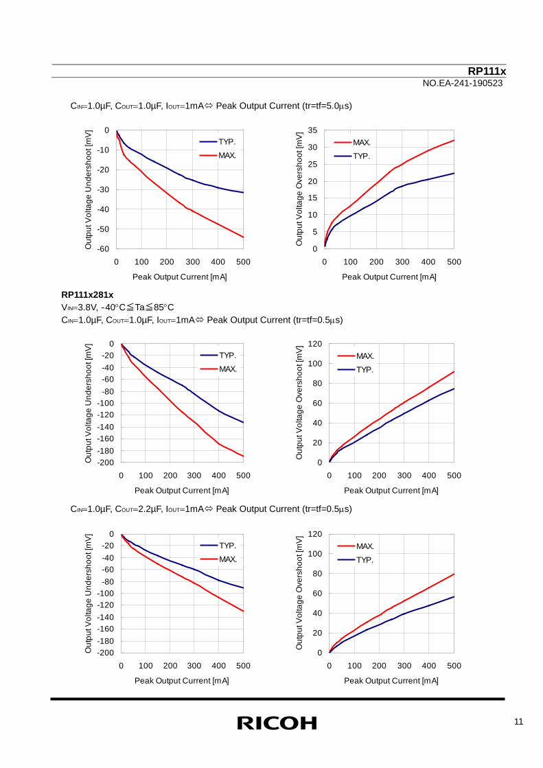
TRANSIENT RESPONSE
The RP111x Series have been improved in overall output voltage characteristics including temperature and transient response. The load transient response indicated under the Electrical Characteristics is guaranteed by design based on the condition when IOUT changes from 1mA to 250mA or 250mA to1mA. The output voltage variations under the other load conditions, the characteristic examples are shown below.
RP111x151x VIN=2.5V, -40°C≦Ta≦85°C CIN=1.0µF, COUT=1.0µF, IOUT=1mAPeak Output Current (tr=tf=0.5µs)
CIN=1.0µF, COUT=2.2µF, IOUT=1mA Peak Output Current (tr=tf=0.5µs)
-200-180-160-140-120-100
-80-60-40-20
0
0 100 200 300 400 500
Peak Output Current [mA]
Out
put V
olta
ge U
nder
shoo
t [m
V]
TYP.MAX.
-200-180-160-140-120-100
-80-60-40-20
0
0 100 200 300 400 500
Peak Output Current [mA]
Out
put V
olta
ge U
nder
shoo
t [m
V]
TYP.MAX.
0
20
40
60
80
100
120
0 100 200 300 400 500
Peak Output Current [mA]
Out
put V
olta
ge O
vers
hoot
[mV] MAX.
TYP.
0
20
40
60
80
100
120
0 100 200 300 400 500
Peak Output Current [mA]
Out
put V
olta
ge O
vers
hoot
[mV] MAX.
TYP.
RP111x NO.EA-241-190523
11
CIN=1.0µF, COUT=1.0µF, IOUT=1mA Peak Output Current (tr=tf=5.0µs) RP111x281x VIN=3.8V, -40°C≦Ta≦85°C CIN=1.0µF, COUT=1.0µF, IOUT=1mA Peak Output Current (tr=tf=0.5µs)
CIN=1.0µF, COUT=2.2µF, IOUT=1mA Peak Output Current (tr=tf=0.5µs)
-60
-50
-40
-30
-20
-10
0
0 100 200 300 400 500
Peak Output Current [mA]
Out
put V
olta
ge U
nder
shoo
t [m
V]
TYP.MAX.
-200-180-160-140-120-100
-80-60-40-20
0
0 100 200 300 400 500
Peak Output Current [mA]
Out
put V
olta
ge U
nder
shoo
t [m
V]
TYP.MAX.
-200-180-160-140-120-100
-80-60-40-20
0
0 100 200 300 400 500
Peak Output Current [mA]
Out
put V
olta
ge U
nder
shoo
t [m
V]
TYP.MAX.
0
20
40
60
80
100
120
0 100 200 300 400 500
Peak Output Current [mA]
Out
put V
olta
ge O
vers
hoot
[mV] MAX.
TYP.
0
20
40
60
80
100
120
0 100 200 300 400 500
Peak Output Current [mA]
Out
put V
olta
ge O
vers
hoot
[mV] MAX.
TYP.
0
5
10
15
20
25
30
35
0 100 200 300 400 500
Peak Output Current [mA]
Out
put V
olta
ge O
vers
hoot
[mV] MAX.
TYP.
RP111x NO.EA-241-190523
12
CIN=1.0µF, COUT=1.0µF, IOUT=1mA Peak Output Current (tr=tf=5.0µs)
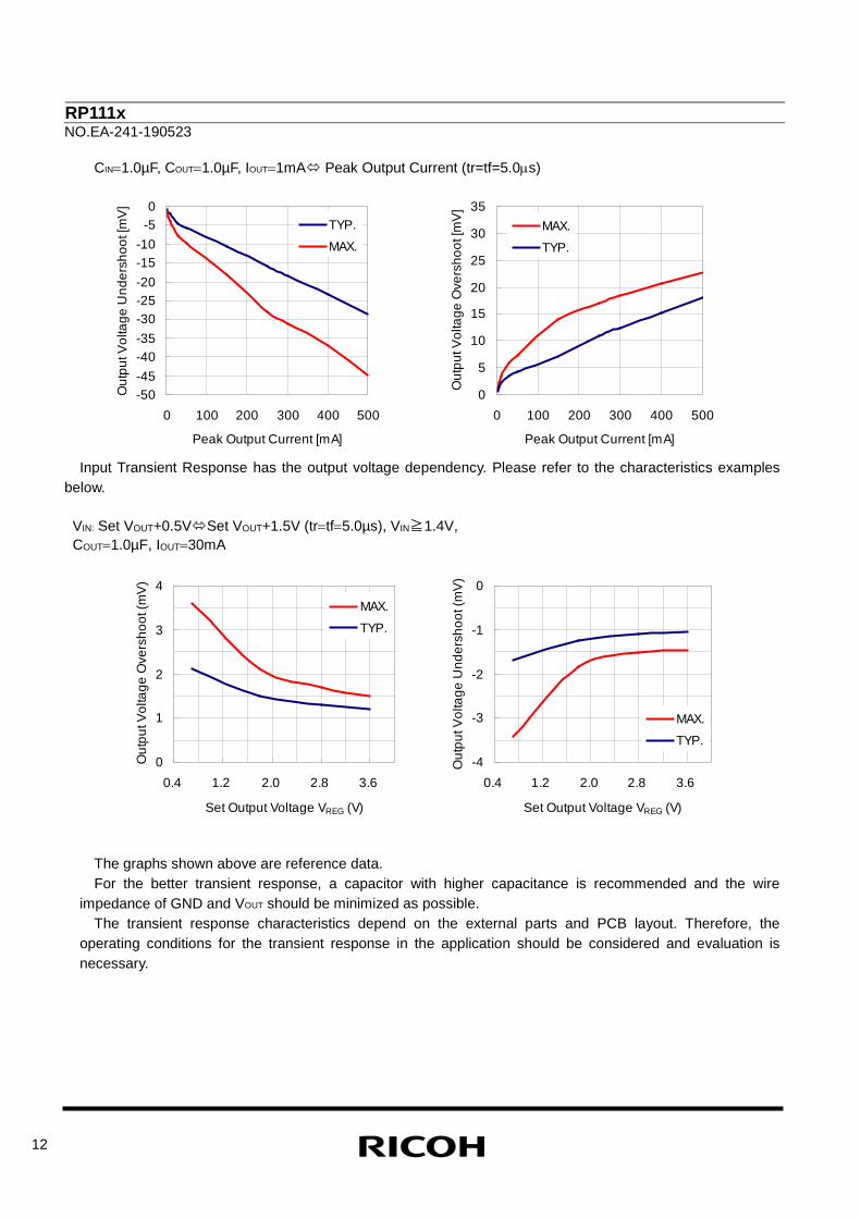
Input Transient Response has the output voltage dependency. Please refer to the characteristics examples below.
VIN: Set VOUT+0.5VSet VOUT+1.5V (tr=tf=5.0µs), VIN≧1.4V, COUT=1.0µF, IOUT=30mA
The graphs shown above are reference data. For the better transient response, a capacitor with higher capacitance is recommended and the wire
impedance of GND and VOUT should be minimized as possible. The transient response characteristics depend on the external parts and PCB layout. Therefore, the
operating conditions for the transient response in the application should be considered and evaluation is necessary.
0
1
2
3
4
0.4 1.2 2.0 2.8 3.6
Set Output Voltage VREG (V)
Out
put V
olta
ge O
vers
hoot
(mV)
MAX.TYP.
-4
-3
-2
-1
0
0.4 1.2 2.0 2.8 3.6
Set Output Voltage VREG (V)
Out
put V
olta
ge U
nder
shoo
t (m
V)
MAX.TYP.
-50-45-40-35-30-25-20-15-10
-50
0 100 200 300 400 500
Peak Output Current [mA]
Out
put V
olta
ge U
nder
shoo
t [m
V]
TYP.MAX.
0
5
10
15
20
25
30
35
0 100 200 300 400 500
Peak Output Current [mA]O
utpu
t Vol
tage
Ove
rsho
ot [m
V] MAX.TYP.
RP111x NO.EA-241-190523
13
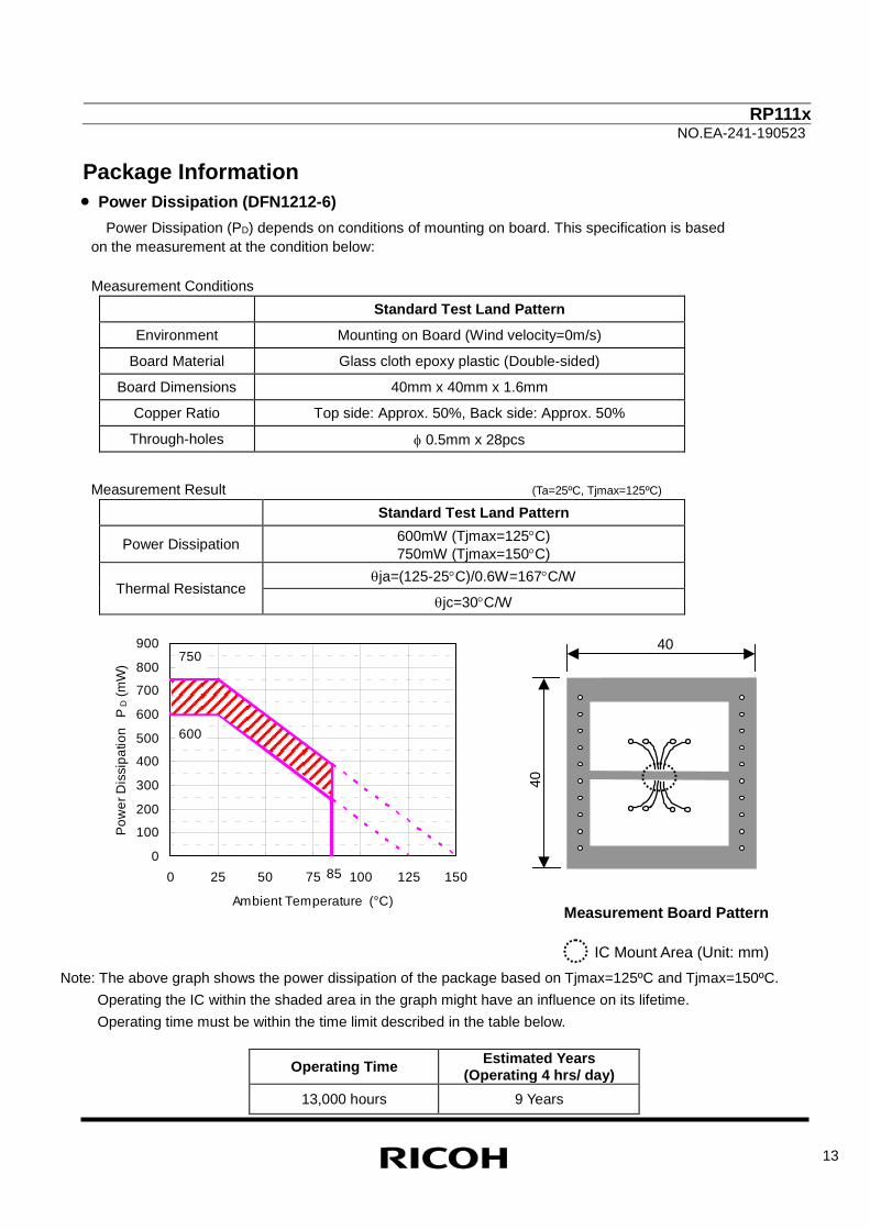
Measurement Board Pattern
IC Mount Area (Unit: mm)
40
40
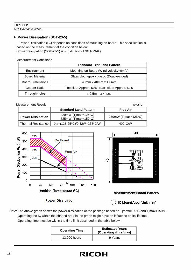
Package Information • Power Dissipation (DFN1212-6)
Power Dissipation (PD) depends on conditions of mounting on board. This specification is based on the measurement at the condition below: Measurement Conditions
Standard Test Land Pattern Environment Mounting on Board (Wind velocity=0m/s)
Board Material Glass cloth epoxy plastic (Double-sided)
Board Dimensions 40mm x 40mm x 1.6mm
Copper Ratio Top side: Approx. 50%, Back side: Approx. 50%
Through-holes φ 0.5mm x 28pcs
Measurement Result (Ta=25ºC, Tjmax=125ºC)
Standard Test Land Pattern
Power Dissipation 600mW (Tjmax=125°C) 750mW (Tjmax=150°C)
Thermal Resistance θja=(125-25°C)/0.6W=167°C/W
θjc=30°C/W
Note: The above graph shows the power dissipation of the package based on Tjmax=125ºC and Tjmax=150ºC. Operating the IC within the shaded area in the graph might have an influence on its lifetime. Operating time must be within the time limit described in the table below.
0
100
200
300
400
500
600
700
800
900
0 25 50 75 100 125 150
Ambient Temperature (°C)
Pow
er D
issi
patio
n P
D (m
W)
85
600
750
Operating Time Estimated Years (Operating 4 hrs/ day)
13,000 hours 9 Years
RP111x NO.EA-241-190523
14
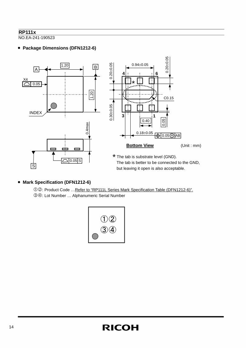
• Package Dimensions (DFN1212-6)
1.20
1.20 A B
0.05 X4
INDEX
S 0.05 S
1
6 4 0.20
± 0.0
5
0.18±0.05 0.05 M AB
C0.15
0.94±0.05
0.30
±0.0
5
0.4m
ax
0.20
±0.0
5
0.40 3
0.05
*
(Unit : mm) Bottom View
* The tab is substrate level (GND). The tab is better to be connected to the GND, but leaving it open is also acceptable.
• Mark Specification (DFN1212-6)
: Product Code …Refer to “RP111L Series Mark Specification Table (DFN1212-6)”. : Lot Number … Alphanumeric Serial Number
①② ③④
RP111x NO.EA-241-190523
15
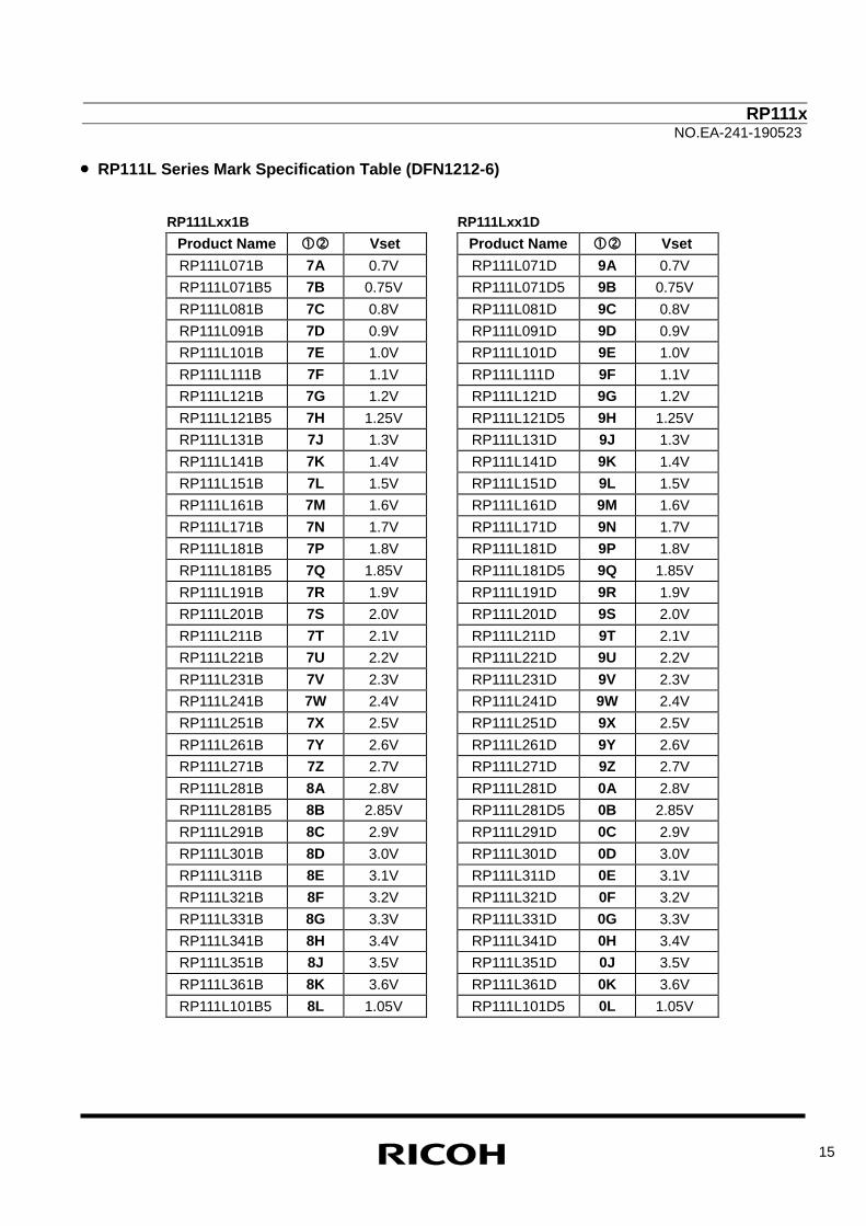
• RP111L Series Mark Specification Table (DFN1212-6)
RP111Lxx1B RP111Lxx1D Product Name Vset Product Name Vset RP111L071B 7A 0.7V RP111L071D 9A 0.7V RP111L071B5 7B 0.75V RP111L071D5 9B 0.75V RP111L081B 7C 0.8V
RP111L081D 9C 0.8V RP111L091B 7D 0.9V RP111L091D 9D 0.9V RP111L101B 7E 1.0V RP111L101D 9E 1.0V RP111L111B 7F 1.1V RP111L111D 9F 1.1V RP111L121B 7G 1.2V RP111L121D 9G 1.2V RP111L121B5 7H 1.25V RP111L121D5 9H 1.25V RP111L131B 7J 1.3V RP111L131D 9J 1.3V RP111L141B 7K 1.4V RP111L141D 9K 1.4V RP111L151B 7L 1.5V RP111L151D 9L 1.5V RP111L161B 7M 1.6V RP111L161D 9M 1.6V RP111L171B 7N 1.7V RP111L171D 9N 1.7V RP111L181B 7P 1.8V RP111L181D 9P 1.8V RP111L181B5 7Q 1.85V RP111L181D5 9Q 1.85V RP111L191B 7R 1.9V RP111L191D 9R 1.9V RP111L201B 7S 2.0V RP111L201D 9S 2.0V RP111L211B 7T 2.1V RP111L211D 9T 2.1V RP111L221B 7U 2.2V RP111L221D 9U 2.2V RP111L231B 7V 2.3V RP111L231D 9V 2.3V RP111L241B 7W 2.4V RP111L241D 9W 2.4V RP111L251B 7X 2.5V RP111L251D 9X 2.5V RP111L261B 7Y 2.6V RP111L261D 9Y 2.6V RP111L271B 7Z 2.7V RP111L271D 9Z 2.7V RP111L281B 8A 2.8V RP111L281D 0A 2.8V RP111L281B5 8B 2.85V RP111L281D5 0B 2.85V RP111L291B 8C 2.9V RP111L291D 0C 2.9V RP111L301B 8D 3.0V RP111L301D 0D 3.0V RP111L311B 8E 3.1V RP111L311D 0E 3.1V RP111L321B 8F 3.2V RP111L321D 0F 3.2V RP111L331B 8G 3.3V RP111L331D 0G 3.3V RP111L341B 8H 3.4V RP111L341D 0H 3.4V RP111L351B 8J 3.5V RP111L351D 0J 3.5V RP111L361B 8K 3.6V RP111L361D 0K 3.6V RP111L101B5 8L 1.05V RP111L101D5 0L 1.05V
RP111x NO.EA-241-190523
16
• Power Dissipation (SOT-23-5) Power Dissipation (PD) depends on conditions of mounting on board. This specification is
based on the measurement at the condition below: (Power Dissipation (SOT-23-5) is substitution of SOT-23-6.) Measurement Conditions
Standard Test Land Pattern Environment Mounting on Board (Wind velocity=0m/s)
Board Material Glass cloth epoxy plastic (Double-sided)
Board Dimensions 40mm x 40mm x 1.6mm
Copper Ratio Top side: Approx. 50%, Back side: Approx. 50%
Through-holes φ 0.5mm x 44pcs
Measurement Result (Ta=25°C)
Standard Land Pattern Free Air
Power Dissipation 420mW (Tjmax=125°C) 525mW (Tjmax=150°C) 250mW (Tjmax=125°C)
Thermal Resistance θja=(125-25°C)/0.42W=238°C/W 400°C/W
Note: The above graph shows the power dissipation of the package based on Tjmax=125ºC and Tjmax=150ºC.
Operating the IC within the shaded area in the graph might have an influence on its lifetime. Operating time must be within the time limit described in the table below.
Operating Time Estimated Years (Operating 4 hrs/ day)
13,000 hours 9 Years
RP111x NO.EA-241-190523
17
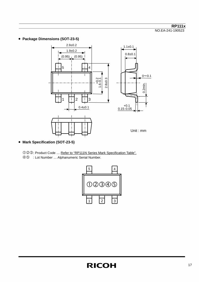
• Package Dimensions (SOT-23-5)
2.9±0.2 1.9±0.2
(0.95) (0.95)
5 4
1 2 3 1.
6-0.
1 +0
.2
2.8±
0.3
0.4±0.1
0.8±0.1
1.1±0.1
0~0.1
0.15-0.05 +0.1
Unit : mm
0.2m
in.
• Mark Specification (SOT-23-5)
: Product Code … Refer to “RP111N Series Mark Specification Table”. : Lot Number … Alphanumeric Serial Number.
5 4
1 2 3
RP111x NO.EA-241-190523
18
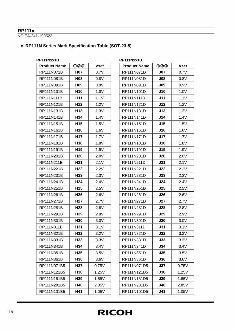
• RP111N Series Mark Specification Table (SOT-23-5)
RP111Nxx1B RP111Nxx1D Product Name Vset Product Name Vset RP111N071B H07 0.7V RP111N071D J07 0.7V RP111N081B H08 0.8V
RP111N081D J08 0.8V RP111N091B H09 0.9V RP111N091D J09 0.9V RP111N101B H10 1.0V RP111N101D J10 1.0V RP111N111B H11 1.1V RP111N111D J11 1.1V RP111N121B H12 1.2V RP111N121D J12 1.2V RP111N131B H13 1.3V RP111N131D J13 1.3V RP111N141B H14 1.4V RP111N141D J14 1.4V RP111N151B H15 1.5V RP111N151D J15 1.5V RP111N161B H16 1.6V RP111N161D J16 1.6V RP111N171B H17 1.7V RP111N171D J17 1.7V RP111N181B H18 1.8V RP111N181D J18 1.8V RP111N191B H19 1.9V RP111N191D J19 1.9V RP111N201B H20 2.0V RP111N201D J20 2.0V RP111N211B H21 2.1V RP111N211D J21 2.1V RP111N221B H22 2.2V RP111N221D J22 2.2V RP111N231B H23 2.3V RP111N231D J23 2.3V RP111N241B H24 2.4V RP111N241D J24 2.4V RP111N251B H25 2.5V RP111N251D J25 2.5V RP111N261B H26 2.6V RP111N261D J26 2.6V RP111N271B H27 2.7V RP111N271D J27 2.7V RP111N281B H28 2.8V RP111N281D J28 2.8V RP111N291B H29 2.9V RP111N291D J29 2.9V RP111N301B H30 3.0V RP111N301D J30 3.0V RP111N311B H31 3.1V RP111N311D J31 3.1V RP111N321B H32 3.2V RP111N321D J32 3.2V RP111N331B H33 3.3V RP111N331D J33 3.3V RP111N341B H34 3.4V RP111N341D J34 3.4V RP111N351B H35 3.5V RP111N351D J35 3.5V RP111N361B H36 3.6V RP111N361D J36 3.6V RP111N071B5 H37 0.75V RP111N071D5 J37 0.75V RP111N121B5 H38 1.25V RP111N121D5 J38 1.25V RP111N181B5 H39 1.85V RP111N181D5 J39 1.85V RP111N281B5 H40 2.85V RP111N281D5 J40 2.85V RP111N101B5 H41 1.05V RP111N101D5 J41 1.05V
RP111x NO.EA-241-190523
19
30 7.5 15
30
7.5
50
50
High Wattage Standard
15
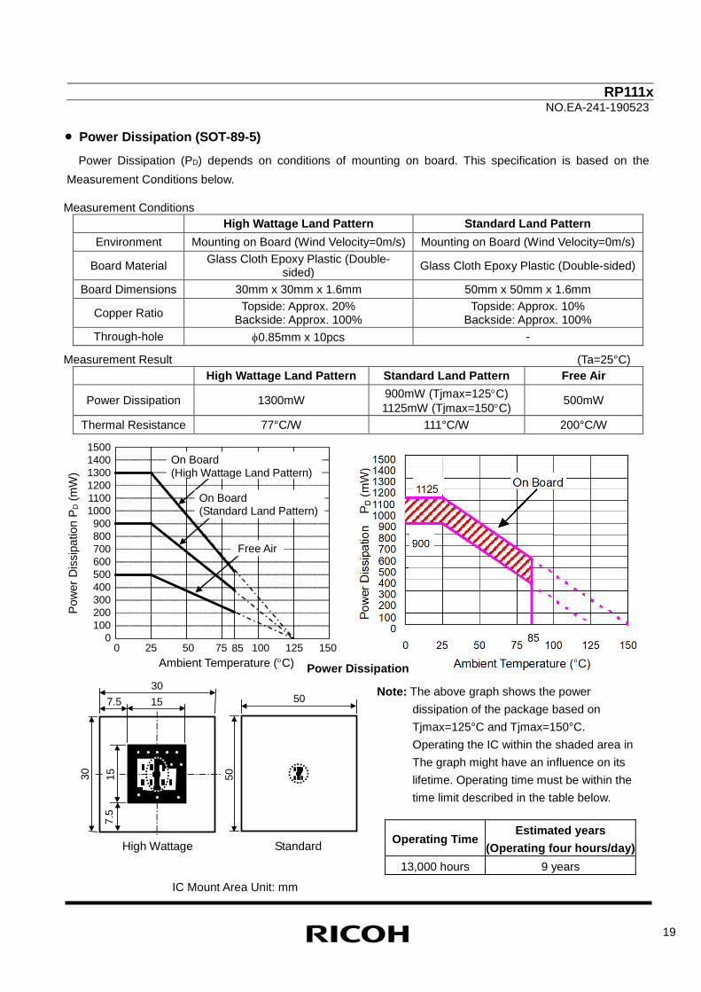
• Power Dissipation (SOT-89-5) Power Dissipation (PD) depends on conditions of mounting on board. This specification is based on the
Measurement Conditions below. Measurement Conditions
High Wattage Land Pattern Standard Land Pattern Environment Mounting on Board (Wind Velocity=0m/s) Mounting on Board (Wind Velocity=0m/s)
Board Material Glass Cloth Epoxy Plastic (Double-sided) Glass Cloth Epoxy Plastic (Double-sided)
Board Dimensions 30mm x 30mm x 1.6mm 50mm x 50mm x 1.6mm
Copper Ratio Topside: Approx. 20% Backside: Approx. 100%
Topside: Approx. 10% Backside: Approx. 100%
Through-hole φ0.85mm x 10pcs -
Measurement Result (Ta=25°C) High Wattage Land Pattern Standard Land Pattern Free Air
Power Dissipation 1300mW 900mW (Tjmax=125°C) 1125mW (Tjmax=150°C) 500mW
Thermal Resistance 77°C/W 111°C/W 200°C/W
Power Dissipation
Measurement Board Pattern
Note: The above graph shows the power dissipation of the package based on Tjmax=125°C and Tjmax=150°C. Operating the IC within the shaded area in The graph might have an influence on its lifetime. Operating time must be within the time limit described in the table below.
Operating Time Estimated years
(Operating four hours/day) 13,000 hours 9 years
Pow
er D
issi
patio
n P D
(mW
)
1500 1400 1300 1200 1100 1000 900 800 700 600 500 400 300 200 100
0 0 25 50 75 100 125 150
Ambient Temperature (°C) 85
On Board (Standard Land Pattern)
On Board (High Wattage Land Pattern)
Free Air
IC Mount Area Unit: mm
RP111x NO.EA-241-190523
20
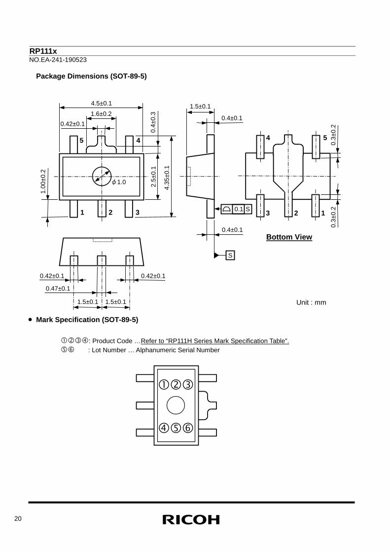
Package Dimensions (SOT-89-5)
1.5±0.1 1.5±0.1
0.47±0.1
0.42±0.1 0.42±0.1
1.5±0.1
0.4±0.1
0.4±0.1
0.1 S
S
0.3±
0.2
0.3±
0.2
4 5
3 2 1
Bottom View
0.42±0.1
4.5±0.1 1.6±0.2
4.35
±0.1
2.5±
0.1
0.4±
0.3
5 4
1 2 3
φ1.0
1.00
±0.2
Unit : mm
• Mark Specification (SOT-89-5) : Product Code …Refer to “RP111H Series Mark Specification Table”. : Lot Number … Alphanumeric Serial Number
RP111x NO.EA-241-190523
21
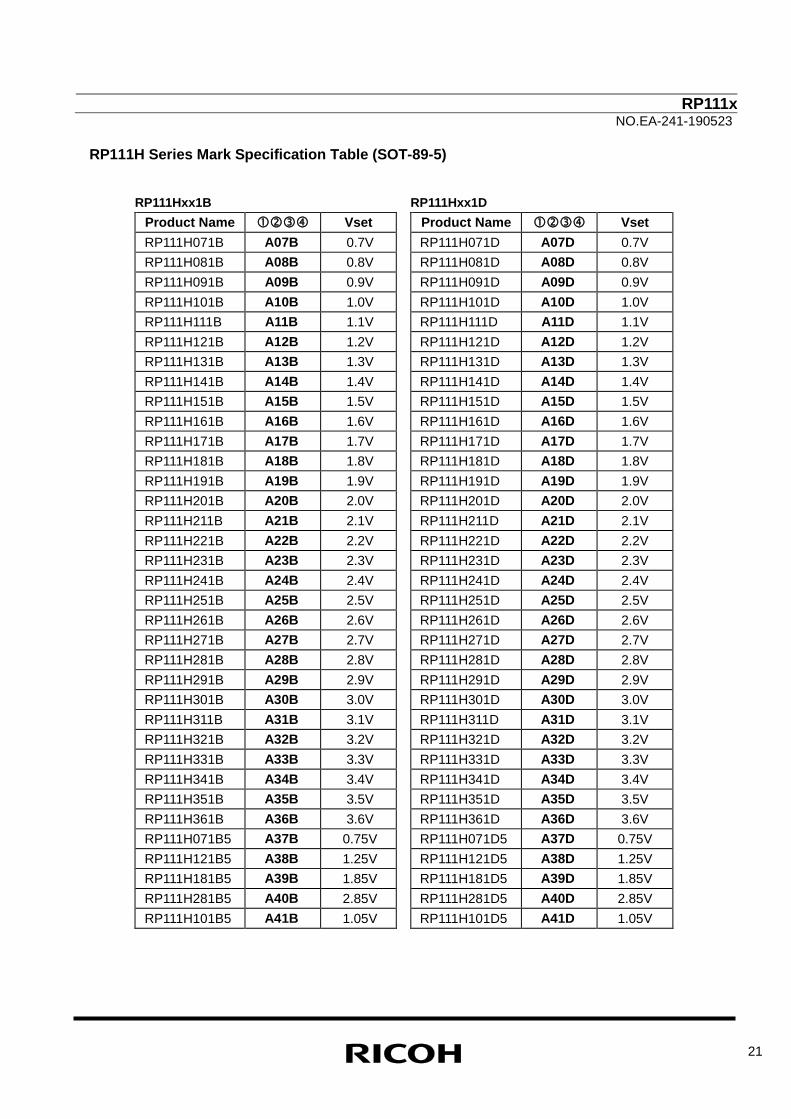
RP111H Series Mark Specification Table (SOT-89-5)
RP111Hxx1B RP111Hxx1D Product Name Vset Product Name Vset RP111H071B A07B 0.7V
RP111H071D A07D 0.7V RP111H081B A08B 0.8V RP111H081D A08D 0.8V RP111H091B A09B 0.9V RP111H091D A09D 0.9V RP111H101B A10B 1.0V RP111H101D A10D 1.0V RP111H111B A11B 1.1V RP111H111D A11D 1.1V RP111H121B A12B 1.2V RP111H121D A12D 1.2V RP111H131B A13B 1.3V RP111H131D A13D 1.3V RP111H141B A14B 1.4V RP111H141D A14D 1.4V RP111H151B A15B 1.5V RP111H151D A15D 1.5V RP111H161B A16B 1.6V RP111H161D A16D 1.6V RP111H171B A17B 1.7V RP111H171D A17D 1.7V RP111H181B A18B 1.8V RP111H181D A18D 1.8V RP111H191B A19B 1.9V RP111H191D A19D 1.9V RP111H201B A20B 2.0V RP111H201D A20D 2.0V RP111H211B A21B 2.1V RP111H211D A21D 2.1V RP111H221B A22B 2.2V RP111H221D A22D 2.2V RP111H231B A23B 2.3V RP111H231D A23D 2.3V RP111H241B A24B 2.4V RP111H241D A24D 2.4V RP111H251B A25B 2.5V RP111H251D A25D 2.5V RP111H261B A26B 2.6V RP111H261D A26D 2.6V RP111H271B A27B 2.7V RP111H271D A27D 2.7V RP111H281B A28B 2.8V RP111H281D A28D 2.8V RP111H291B A29B 2.9V RP111H291D A29D 2.9V RP111H301B A30B 3.0V RP111H301D A30D 3.0V RP111H311B A31B 3.1V RP111H311D A31D 3.1V RP111H321B A32B 3.2V RP111H321D A32D 3.2V RP111H331B A33B 3.3V RP111H331D A33D 3.3V RP111H341B A34B 3.4V RP111H341D A34D 3.4V RP111H351B A35B 3.5V RP111H351D A35D 3.5V RP111H361B A36B 3.6V RP111H361D A36D 3.6V RP111H071B5 A37B 0.75V RP111H071D5 A37D 0.75V RP111H121B5 A38B 1.25V RP111H121D5 A38D 1.25V RP111H181B5 A39B 1.85V RP111H181D5 A39D 1.85V RP111H281B5 A40B 2.85V RP111H281D5 A40D 2.85V RP111H101B5 A41B 1.05V RP111H101D5 A41D 1.05V
RP111x NO.EA-241-190523
22
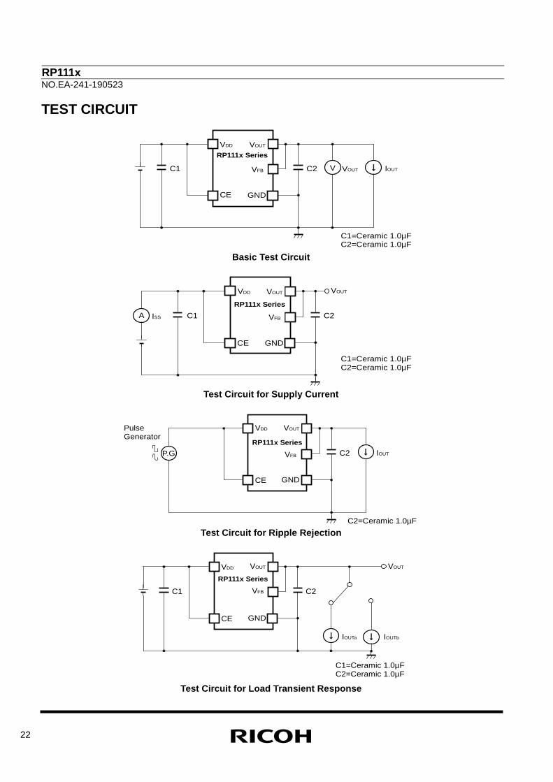
TEST CIRCUIT
C1
RP111x Series VDD VOUT
CE GND
V C2 VOUT IOUT
C1=Ceramic 1.0µF C2=Ceramic 1.0µF
VFB ↓
Basic Test Circuit
VOUT
C1
VDD VOUT
CE GND
C2 A ISS RP111x Series
C1=Ceramic 1.0µF C2=Ceramic 1.0µF
VFB
Test Circuit for Supply Current
RP111x Series
VDD VOUT
CE GND
C2
Pulse Generator
IOUT
C2=Ceramic 1.0µF
P.G. ↓ VFB
Test Circuit for Ripple Rejection
IOUTa IOUTb
C1 RP111x Series VDD VOUT
CE GND
C2
↓
C1=Ceramic 1.0µF C2=Ceramic 1.0µF
↓
VOUT
VFB
Test Circuit for Load Transient Response
RP111x NO.EA-241-190523
23
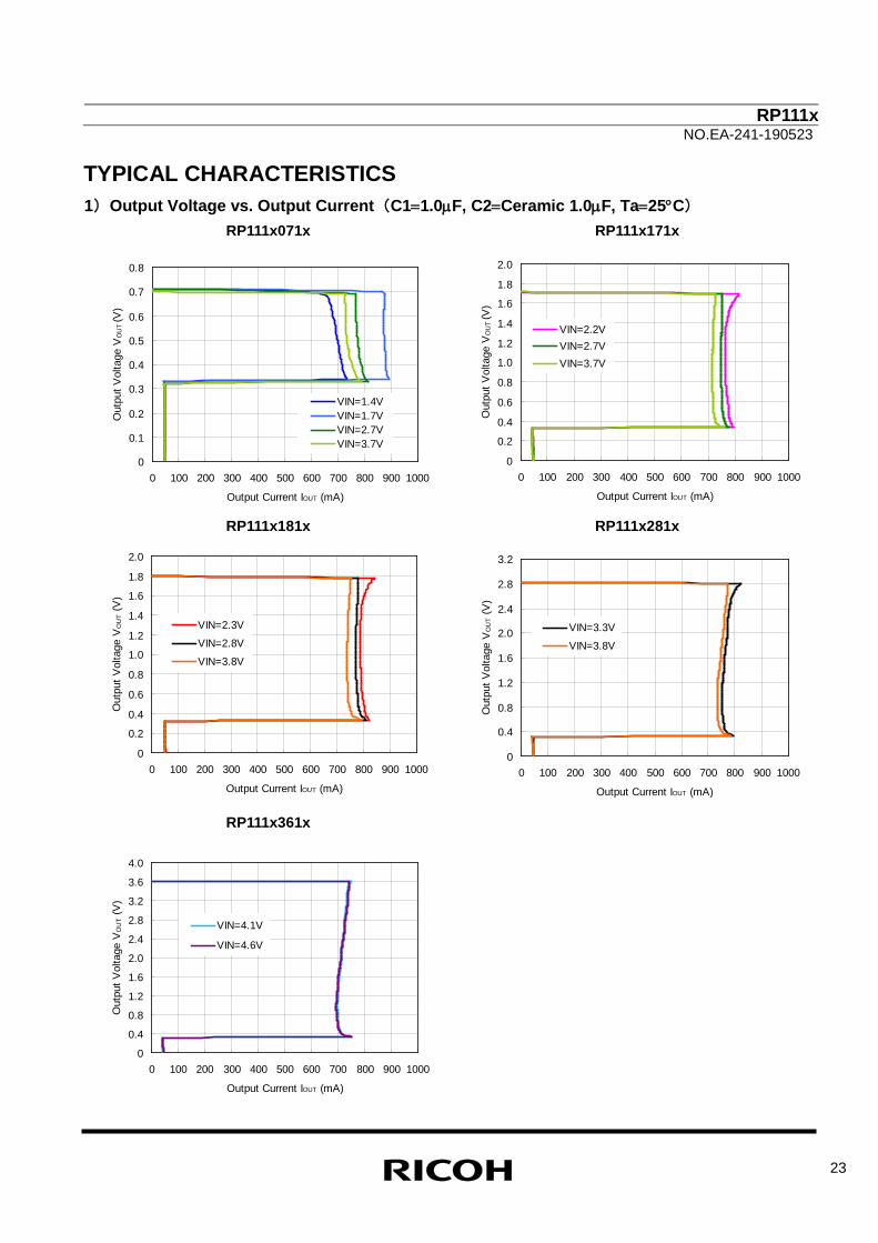
TYPICAL CHARACTERISTICS 1) Output Voltage vs. Output Current (C1=1.0µF, C2=Ceramic 1.0µF, Ta=25°C) RP111x071x RP111x171x
RP111x181x RP111x281x
RP111x361x
0
0.1
0.2
0.3
0.4
0.5
0.6
0.7
0.8
0 100 200 300 400 500 600 700 800 900 1000
Output Current IOUT (mA)
Out
put V
olta
ge V
OU
T (V
)
VIN=1.4VVIN=1.7VVIN=2.7VVIN=3.7V
0
0.2
0.4
0.6
0.8
1.0
1.2
1.4
1.6
1.8
2.0
0 100 200 300 400 500 600 700 800 900 1000
Output Current IOUT (mA)O
utpu
t Vol
tage
VO
UT (V
)
VIN=2.2VVIN=2.7VVIN=3.7V
0
0.2
0.4
0.6
0.8
1.0
1.2
1.4
1.6
1.8
2.0
0 100 200 300 400 500 600 700 800 900 1000
Output Current IOUT (mA)
Out
put V
olta
ge V
OU
T (V
)
VIN=2.3VVIN=2.8VVIN=3.8V
0
0.4
0.8
1.2
1.6
2.0
2.4
2.8
3.2
0 100 200 300 400 500 600 700 800 900 1000
Output Current IOUT (mA)
Out
put V
olta
ge V
OU
T (V
)
VIN=3.3VVIN=3.8V
0
0.4
0.8
1.2
1.6
2.0
2.4
2.8
3.2
3.6
4.0
0 100 200 300 400 500 600 700 800 900 1000
Output Current IOUT (mA)
Out
put V
olta
ge V
OU
T (V
)
VIN=4.1V
VIN=4.6V
RP111x NO.EA-241-190523
24
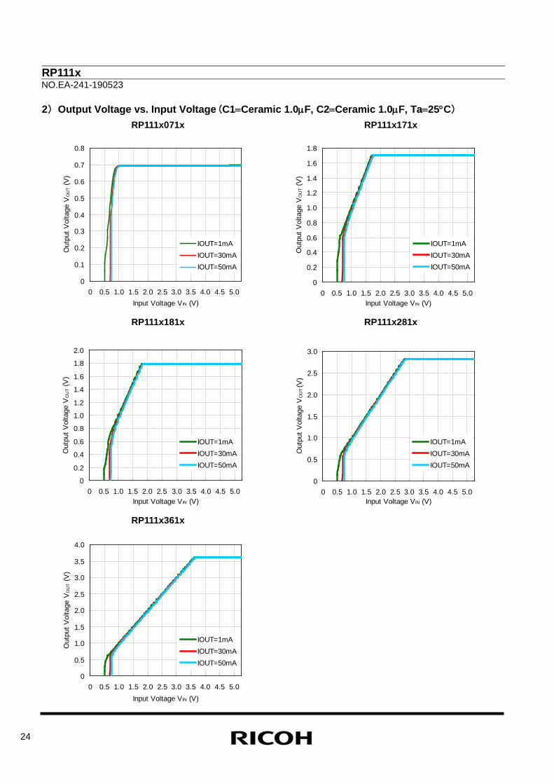
2) Output Voltage vs. Input Voltage (C1=Ceramic 1.0µF, C2=Ceramic 1.0µF, Ta=25°C) RP111x071x RP111x171x
RP111x181x RP111x281x
RP111x361x
0
0.1
0.2
0.3
0.4
0.5
0.6
0.7
0.8
0 0.5 1.0 1.5 2.0 2.5 3.0 3.5 4.0 4.5 5.0Input Voltage VIN (V)
Out
put V
olta
ge V
OU
T (V
)
IOUT=1mAIOUT=30mAIOUT=50mA
0
0.2
0.4
0.6
0.8
1.0
1.2
1.4
1.6
1.8
0 0.5 1.0 1.5 2.0 2.5 3.0 3.5 4.0 4.5 5.0Input Voltage VIN (V)
Out
put V
olta
ge V
OU
T (V
)
IOUT=1mAIOUT=30mAIOUT=50mA
0
0.2
0.4
0.6
0.8
1.0
1.2
1.4
1.6
1.8
2.0
0 0.5 1.0 1.5 2.0 2.5 3.0 3.5 4.0 4.5 5.0Input Voltage VIN (V)
Out
put V
olta
ge V
OU
T (V
)
IOUT=1mAIOUT=30mAIOUT=50mA
0
0.5
1.0
1.5
2.0
2.5
3.0
0 0.5 1.0 1.5 2.0 2.5 3.0 3.5 4.0 4.5 5.0Input Voltage VIN (V)
Out
put V
olta
ge V
OU
T (V
)
IOUT=1mAIOUT=30mAIOUT=50mA
0
0.5
1.0
1.5
2.0
2.5
3.0
3.5
4.0
0 0.5 1.0 1.5 2.0 2.5 3.0 3.5 4.0 4.5 5.0Input Voltage VIN (V)
Out
put V
olta
ge V
OU
T (V
)
IOUT=1mAIOUT=30mAIOUT=50mA
RP111x NO.EA-241-190523
25
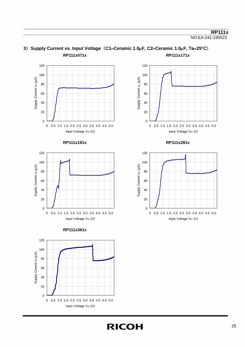
3) Supply Current vs. Input Voltage (C1=Ceramic 1.0µF, C2=Ceramic 1.0µF, Ta=25°C) RP111x071x RP111x171x
RP111x181x RP111x281x
RP111x361x
0
20
40
60
80
100
120
0 0.5 1.0 1.5 2.0 2.5 3.0 3.5 4.0 4.5 5.0
Input Voltage VIN (V)
Sup
ply
Cur
rent
I SS
(µA
)
0
20
40
60
80
100
120
0 0.5 1.0 1.5 2.0 2.5 3.0 3.5 4.0 4.5 5.0
Input Voltage VIN (V)
Sup
ply
Cur
rent
I SS
(µA
)
0
20
40
60
80
100
120
0 0.5 1.0 1.5 2.0 2.5 3.0 3.5 4.0 4.5 5.0
Input Voltage VIN (V)
Sup
ply
Cur
rent
I SS (µ
A)
0
20
40
60
80
100
120
0 0.5 1.0 1.5 2.0 2.5 3.0 3.5 4.0 4.5 5.0
Input Voltage VIN (V)
Sup
ply
Cur
rent
I SS
(µA
)
0
20
40
60
80
100
120
0 0.5 1.0 1.5 2.0 2.5 3.0 3.5 4.0 4.5 5.0
Input Voltage VIN (V)
Sup
ply
Cur
rent
I SS (µ
A)
RP111x NO.EA-241-190523
26
4) Output Voltage vs. Temperature (C1=Ceramic 1.0µF, C2=Ceramic 1.0µF, IOUT=1mA) RP111x071x RP111x171x
RP111x181x RP111x281x
RP111x361x
0.65
0.660.67
0.680.69
0.700.71
0.720.73
0.740.75
-50 -25 0 25 50 75 100
Temperature Topt (゚C)
Out
put V
olta
ge V
OU
T (V
)
VIN=1.7V
1.651.66
1.671.68
1.691.70
1.711.72
1.731.74
1.75
-50 -25 0 25 50 75 100
Temperature Topt (゚C)O
utpu
t Vol
tage
VO
UT
(V)
VIN=2.7V
1.751.76
1.771.78
1.791.80
1.811.82
1.831.84
1.85
-50 -25 0 25 50 75 100
Temperature Topt (゚C)
Out
put V
olta
ge V
OU
T (V
)
VIN=2.8V
2.752.76
2.772.78
2.792.80
2.812.82
2.832.84
2.85
-50 -25 0 25 50 75 100
Temperature Topt (゚C)
Out
put V
olta
ge V
OU
T (V
)
VIN=3.8V
3.553.56
3.573.58
3.593.60
3.613.62
3.633.64
3.65
-50 -25 0 25 50 75 100
Temperature Topt (゚C)
Out
put V
olta
ge V
OU
T (V
)
VIN=4.6V
Temperature Ta (°C)
Ta (°C)
Temperature Ta (°C)
Temperature Ta (°C) Temperature Ta (°C)
Temperature Ta (°C)
RP111x NO.EA-241-190523
27
5) Supply Current vs. Temperature (C1=Ceramic 1.0µF, C2=Ceramic 1.0µF, IOUT=0mA) RP111x071x RP111x171x
RP111x181x RP111x281x
RP111x361x
60
65
70
75
80
85
90
-50 -25 0 25 50 75 100
Temperature Topt (゚C)
Sup
ply
Cur
rent
ISS
(µA
)
VIN=1.7V
60
65
70
75
80
85
90
-50 -25 0 25 50 75 100
Temperature Topt (゚C)
Sup
ply
Cur
rent
ISS
(µA
)
VIN=2.7V
60
65
70
75
80
85
90
-50 -25 0 25 50 75 100
Temperature Topt (゚C)
Sup
ply
Cur
rent
ISS
(µA
)
VIN=2.8V
60
65
70
75
80
85
90
-50 -25 0 25 50 75 100
Temperature Topt (゚C)
Sup
ply
Cur
rent
ISS
(µA
)
VIN=3.8V
60
65
70
75
80
85
90
-50 -25 0 25 50 75 100
Temperature Topt (゚C)
Sup
ply
Cur
rent
ISS
(µA
)
VIN=4.6V
Temperature Ta (°C) Temperature Ta (°C)
Temperature Ta (°C) Temperature Ta (°C)
Temperature Ta (°C)

RP111x NO.EA-241-190523
28
6) Dropout Voltage vs. Output Current (C1=Ceramic 1.0µF, C2=Ceramic 1.0µF) RP111x071x RP111x171x
RP111x181x RP111x281x
RP111x361x
0
100
200
300
400
500
600
700
0 50 100 150 200 250 300 350 400 450 500Output Current IOUT (mA)
Dro
pout
Vol
tage
VD
IF (m
V)
85゚C25゚C-40゚C
0
50
100
150
200
250
300
350
0 50 100 150 200 250 300 350 400 450 500Output Current IOUT(mA)
Dro
pout
Vol
tage
VD
IF (m
V)
85゚C25゚C-40゚C
0
50
100
150
200
250
300
350
0 50 100 150 200 250 300 350 400 450 500Output Current IOUT (mA)
Dro
pout
Vol
tage
VD
IF (m
V) 85゚C
25゚C-40゚C
0
50
100
150
200
250
300
350
0 50 100 150 200 250 300 350 400 450 500
Output Current IOUT (mA)
Dro
pout
Vol
tage
VD
IF (m
V)
85゚C25゚C-40゚C
0
50
100
150
200
250
0 50 100 150 200 250 300 350 400 450 500
Output Current IOUT (mA)
Dro
pout
Vol
tage
VD
IF (m
V)
85゚C25゚C-40゚C

RP111x NO.EA-241-190523
29
7) Dropout Voltage vs. Set Output Voltage (C1=Ceramic 1.0µF, C2=Ceramic 1.0µF, Ta=25°C)
8)Dropout Voltage vs. Temperature(C1=Ceramic 1.0µF, C2=Ceramic 1.0µF) RP111x071x RP111x171xx
RP111x181x RP111x281x
0
100
200
300
400
500
600
0.4 0.8 1.2 1.6 2.0 2.4 2.8 3.2 3.6 4.0Set Output Voltage VREG (V)
Dro
pout
Vol
tage
VD
IF (m
V)
500mA400mA300mA200mA150mA100mA50mA30mA10mA
0
100
200
300
400
500
600
700
-50 -25 0 25 50 75 100Temperature Topt (゚C)
Dro
pout
Vol
tage
VD
IF (m
V)
500mA 400mA300mA 200mA100mA 50mA
0
50
100
150
200
250
300
350
-50 -25 0 25 50 75 100Temperature Topt (゚C)
Dro
pout
Vol
tage
VD
IF (m
V)
500mA 400mA300mA 200mA100mA 50mA
0
50
100
150
200
250
300
350
-50 -25 0 25 50 75 100
Temperature Topt (゚C)
Dro
pout
Vol
tage
VD
IF (m
V)
500mA 400mA300mA 200mA100mA 50mA
0
50
100
150
200
250
300
350
-50 -25 0 25 50 75 100Temperature Topt (゚C)
Dro
pout
Vol
tage
VD
IF (m
V)
500mA 400mA300mA 200mA100mA 50mA
Temperature Ta (°C) Temperature Ta (°C)
Temperature Ta (°C) Temperature Ta (°C)
RP111x NO.EA-241-190523
30
RP111x361x
9) Ripple Rejection vs. Input Voltage (C1=none, C2=Ceramic 1.0µF, Ripple=0.2Vp-p, Ta=25°C) RP111x071x RP111x071x
RP111x171x RP111x171x
0
50
100
150
200
250
300
350
-50 -25 0 25 50 75 100
Temperature Topt (゚C)
Dro
pout
Vol
tage
VD
IF (m
V)
500mA 400mA300mA 200mA100mA 50mA
0
10
20
30
40
50
60
70
80
90
100
0.5 1.0 1.5 2.0 2.5 3.0 3.5 4.0 4.5 5.0Input Voltage VIN (V)
Rip
ple
Rej
ectio
n R
R (d
B)
f=100Hzf=1kHzf=10kHzf=100kHz
IOUT=1mA
0
10
20
30
40
50
60
70
80
90
100
0.5 1.0 1.5 2.0 2.5 3.0 3.5 4.0 4.5 5.0
Input Voltage VIN (V)
Rip
ple
Rej
ectio
n R
R (d
B)
f=100Hzf=1kHzf=10kHzf=100kHz
IOUT=30mA
0
10
20
30
40
50
60
70
80
90
100
1.5 2.0 2.5 3.0 3.5 4.0 4.5 5.0Input Voltage VIN (V)
Rip
ple
Rej
ectio
n R
R (d
B)
f=100Hzf=1kHzf=10kHzf=100kHz
IOUT=1mA
0
10
20
30
40
50
60
70
80
90
100
1.5 2.0 2.5 3.0 3.5 4.0 4.5 5.0 5.5Input Voltage VIN (V)
Rip
ple
Rej
ectio
n R
R (d
B)
f=100Hzf=1kHzf=10kHzf=100kHz
IOUT=30mA
Temperature Ta (°C)
RP111x NO.EA-241-190523
31
RP111x181x RP111x181x
RP111x281x RP111x281x
RP111x361x RP111x361x
0
10
20
30
40
50
60
70
80
90
100
1.5 2.0 2.5 3.0 3.5 4.0 4.5 5.0Input Voltage VIN (V)
Rip
ple
Rej
ectio
n R
R (d
B)
f=100Hzf=1kHzf=10kHzf=100kHz
IOUT=1mA
0
10
20
30
40
50
60
70
80
90
100
1.5 2.0 2.5 3.0 3.5 4.0 4.5 5.0Input Voltage VIN (V)
Rip
ple
Rej
ectio
n R
R (d
B)
f=100Hzf=1kHzf=10kHzf=100kHz
IOUT=30mA
0
10
20
30
40
50
60
70
80
90
100
2.5 3.0 3.5 4.0 4.5 5.0Input Voltage VIN (V)
Rip
ple
Rej
ectio
n R
R (d
B)
f=100Hzf=1kHzf=10kHzf=100kHz
IOUT=1mA
0
10
20
30
40
50
60
70
80
90
100
2.5 3.0 3.5 4.0 4.5 5.0 5.5Input Voltage VIN (V)
Rip
ple
Rej
ectio
n R
R (d
B)
f=100Hzf=1kHzf=10kHzf=100kHz
IOUT=30mA
0
10
20
30
40
50
60
70
80
90
100
3.5 4.0 4.5 5.0Input Voltage VIN (V)
Rip
ple
Rej
ectio
n R
R (d
B)
f=100Hzf=1kHzf=10kHzf=100kHz
IOUT=1mA
0
10
20
30
40
50
60
70
80
90
100
3.5 4.0 4.5 5.0Input Voltage VIN (V)
Rip
ple
Rej
ectio
n R
R (d
B)
f=100Hzf=1kHzf=10kHzf=100kHz
IOUT=30mA
RP111x NO.EA-241-190523
32
10)Ripple Rejection vs. Frequency (C1=none, C2=Ceramic 1.0µF, Ripple=0.2Vp-p, Ta=25°C) RP111x071x RP111x171x
RP111x181x RP111x281x
RP111x361x
010
203040
5060
708090
100110
0.1 1 10 100 1000Frequency f (kHz)
Rip
ple
Rej
ectio
n R
R (d
B)
1mA30mA150mA
VIN=1.7V
010
203040
5060
708090
100110
0.1 1 10 100 1000Frequency f (kHz)
Rip
ple
Rej
ectio
n R
R (d
B)
1mA30mA150mA
VIN=2.7V
010
20304050
60708090
100110
0.1 1 10 100 1000Frequency f (kHz)
Rip
ple
Rej
ectio
n R
R (d
B)
1mA30mA150mA
VIN=2.8V
01020304050
60708090
100110
0.1 1 10 100 1000Frequency f (kHz)
Rip
ple
Rej
ectio
n R
R (d
B)
1mA30mA150mA
VIN=3.8V
010
203040
5060
708090
100110
0.1 1 10 100 1000Frequency f (kHz)
Rip
ple
Rej
ectio
n R
R (d
B)
1mA30mA150mA
VIN=4.6V
RP111x NO.EA-241-190523
33
11) Input Transient Response (C1=none, C2=Ceramic 1.0µF, IOUT=30mA, tr=tf=5µs, Ta=25°C) RP111x071x RP111x171x
RP111x181x RP111x281x
RP111x361x
0.6850.6900.6950.7000.705
0 10 20 30 40 50 60 70 80 90 100
Time t (µs)
Out
put V
olta
ge V
OU
T (V
)
1.01.52.02.53.0
Inpu
t Vol
tage
VIN
(V)
Output Voltage
Input Voltage1.4V ⇔ 2.4V
1.6851.6901.6951.7001.705
0 10 20 30 40 50 60 70 80 90 100
Time t (µs)
Out
put V
olta
ge V
OU
T (V
)
1.01.52.02.53.03.5
Inpu
t Vol
tage
VIN
(V)
Output Voltage
Input Voltage2.2V ⇔ 3.2V
1.7851.7901.7951.8001.805
0 10 20 30 40 50 60 70 80 90 100
Time t (µs)
Out
put V
olta
ge V
OU
T (V
)
1.01.52.02.53.03.5
Inpu
t Vol
tage
VIN
(V)
Output Voltage
Input Voltage2.3V ⇔ 3.3V
2.7852.7902.7952.8002.805
0 10 20 30 40 50 60 70 80 90 100
Time t (µs)
Out
put V
olta
ge V
OU
T (V
)
1.01.52.02.53.03.54.04.5
Inpu
t Vol
tage
VIN
(V)
Output Voltage
Input Voltage3.3V ⇔ 4.3V
3.5853.5903.5953.6003.605
0 10 20 30 40 50 60 70 80 90 100
Time t (µs)
Out
put V
olta
ge V
OU
T (V
)
1.01.52.02.53.03.54.04.55.05.5
Inpu
t Vol
tage
VIN
(V)
Output Voltage
Input Voltage4.1V ⇔ 5.1V
RP111x NO.EA-241-190523
34
12) Load Transient Response (C1=Ceramic 1.0µF, C2=Ceramic 1.0µF, Ta=25°C) RP111x071x RP111x071x
RP111x071x RP111x071x
RP111x071x RP111x071x
0.670.680.690.700.710.72
0 5 10 15 20 25 30 35 40 45 50
Time t (µs)
Out
put V
olta
ge V
OU
T (V
)
050100150
Out
put C
urre
nt I O
UT
(mA
)Output Voltage
Output Current50mA ⇔ 100mA
tr=tf=0.5Vµs,VIN=1.7V
0.670.680.690.700.710.72
0 20 40 60 80 100 120 140 160 180 200
Time t (µs)O
utpu
t Vol
tage
VO
UT
(V)
050100150
Out
put C
urre
nt I O
UT (m
A)
Output Voltage
Output Current50mA ⇔ 100mA
tr=tf=5.0µs,VIN=1.7V
0.640.660.680.700.720.74
0 20 40 60 80 100 120 140 160
Time t (µs)
Out
put V
olta
ge V
OU
T (V
)
050100150200
Out
put C
urre
nt I O
UT
(mA
)
Output Voltage
Output Current1mA ⇔ 150mA
tr=tf=0.5Vµs,VIN=1.7V
0.670.680.690.700.710.72
0 20 40 60 80 100 120 140 160 180 200
Time t (µs)
Out
put V
olta
ge V
OU
T (V
)
050100150200
Out
put C
urre
nt I O
UT
(mA
)
Output Voltage
Output Current1mA ⇔ 150mA
tr=tf=5.0µs,VIN=1.7V
0.550.600.650.700.750.80
0 20 40 60 80 100 120 140 160
Time t (µs)
Out
put V
olta
ge V
OU
T (V
)
0100200300
Out
put C
urre
nt I O
UT
(mA
)
Output Voltage
Output Current1mA ⇔ 250mA
tr=tf=0.5Vµs,VIN=1.7V
0.670.680.690.700.710.72
0 20 40 60 80 100 120 140 160 180 200
Time t (µs)
Out
put V
olta
ge V
OU
T (V
)
0100200300
Out
put C
urre
nt I O
UT
(mA
)
Output Voltage
Output Current1mA ⇔ 250mA
tr=tf=5.0µs,VIN=1.7V
RP111x NO.EA-241-190523
35
RP111x171x RP111x171x
RP111x171x RP111x171x
RP111x171x RP111x171x
1.671.681.691.701.711.72
0 5 10 15 20 25 30 35 40 45 50
Time t (µs)
Out
put V
olta
ge V
OU
T (V
)
050100150
Out
put C
urre
nt I O
UT
(mA
)
Output Voltage
Output Current50mA ⇔ 100mA
tr=tf=0.5µs,VIN=2.7V
1.671.681.691.701.711.72
0 20 40 60 80 100 120 140 160 180 200
Time t (µs)
Out
put V
olta
ge V
OU
T (V
)
050100150
Out
put C
urre
nt I O
UT
(mA
)
Output Voltage
Output Current50mA ⇔ 100mA
tr=tf=5.0µs,VIN=2.7V
1.641.661.681.701.721.74
0 20 40 60 80 100 120 140 160
Time t (µs)
Out
put V
olta
ge V
OU
T (V
)
050100150200
Out
put C
urre
nt I O
UT (m
A)
Output Voltage
Output Current1mA ⇔ 150mA
tr=tf=0.5µs,VIN=2.7V
1.671.681.691.701.711.72
0 20 40 60 80 100 120 140 160 180 200
Time t (µs)
Out
put V
olta
ge V
OU
T (V
)
050100150200
Out
put C
urre
nt I O
UT
(mA
)
Output Voltage
Output Current1mA ⇔ 150mA
tr=tf=5.0µs,VIN=2.7V
1.551.601.651.701.751.80
0 20 40 60 80 100 120 140 160
Time t (µs)
Out
put V
olta
ge V
OU
T (V
)
0100200300
Out
put C
urre
nt I O
UT
(mA
)
Output Voltage
Output Current1mA ⇔ 250mA
tr=tf=0.5µs,VIN=2.7V
1.671.681.691.701.711.72
0 20 40 60 80 100 120 140 160 180 200
Time t (µs)
Out
put V
olta
ge V
OU
T (V
)
0100200300
Out
put C
urre
nt I O
UT
(mA
)
Output Voltage
Output Current1mA ⇔ 250mA
tr=tf=5.0µs,VIN=2.7V
RP111x NO.EA-241-190523
36
RP111x181x RP111x181x
RP111x181x RP111x181x
RP111x181x RP111x181x
1.771.781.791.801.811.82
0 5 10 15 20 25 30 35 40 45 50
Time t (µs)
Out
put V
olta
ge V
OU
T (V
)
050100150
Out
put C
urre
nt I O
UT
(mA
)
Output Voltage
Output Current50mA ⇔ 100mA
tr=tf=0.5µs,VIN=2.8V
1.771.781.791.801.811.82
0 20 40 60 80 100 120 140 160 180 200
Time t (µs)
Out
put V
olta
ge V
OU
T (V
)
050100150
Out
put C
urre
nt I O
UT (m
A)
Output Voltage
Output Current50mA ⇔ 100mA
tr=tf=5.0µs,VIN=2.8V
1.741.761.781.801.821.84
0 20 40 60 80 100 120 140 160
Time t (µs)
Out
put V
olta
ge V
OU
T (V
)
050100150200
Out
put C
urre
nt I O
UT
(mA
)
Output Voltage
Output Current1mA ⇔ 150mA
tr=tf=0.5µs,VIN=2.8V
1.771.781.791.801.811.82
0 20 40 60 80 100 120 140 160 180 200
Time t (µs)
Out
put V
olta
ge V
OU
T (V
)
050100150200
Out
put C
urre
nt I O
UT
(mA
)
Output Voltage
Output Current1mA ⇔ 150mA
tr=tf=5.0µs,VIN=2.8V
1.651.701.751.801.85
0 20 40 60 80 100 120 140 160
Time t (µs)
Out
put V
olta
ge V
OU
T (V
)
0100200300
Out
put C
urre
nt I O
UT
(mA
)
Output Voltage
Output Current1mA ⇔ 250mA
tr=tf=0.5µs,VIN=2.8V
1.771.781.791.801.811.82
0 20 40 60 80 100 120 140 160 180 200
Time t (µs)
Out
put V
olta
ge V
OU
T (V
)
0100200300
Out
put C
urre
nt I O
UT
(mA
)
Output Voltage
Output Current1mA ⇔ 250mA
tr=tf=5.0µs,VIN=2.8V

RP111x NO.EA-241-190523
37
RP111x281x RP111x281x
RP111x281x RP111x281x
RP111x281x RP111x281x
2.772.782.792.802.812.82
0 5 10 15 20 25 30 35 40 45 50
Time t (µs)
Out
put V
olta
ge V
OU
T (V
)
050100150
Out
put C
urre
nt I O
UT
(mA
)
Output Voltage
Output Current50mA ⇔ 100mA
tr=tf=0.5µs,VIN=3.8V
2.772.782.792.802.812.82
0 20 40 60 80 100 120 140 160 180 200
Time t (µs)
Out
put V
olta
ge V
OU
T (V
)
050100150
Out
put C
urre
nt I O
UT
(mA
)
Output Voltage
Output Current50mA ⇔ 100mA
tr=tf=5.0µs,VIN=3.8V
2.742.762.782.802.822.84
0 20 40 60 80 100 120 140 160
Time t (µs)
Out
put V
olta
ge V
OU
T (V
)
050100150200
Out
put C
urre
nt I O
UT
(mA
)
Output Voltage
Output Current1mA ⇔ 150mA
tr=tf=0.5µs,VIN=3.8V
2.772.782.792.802.812.82
0 20 40 60 80 100 120 140 160 180 200
Time t (µs)
Out
put V
olta
ge V
OU
T (V
)
050100150200
Out
put C
urre
nt I O
UT
(mA
)
Output Voltage
Output Current1mA ⇔ 150mA
tr=tf=5.0µs,VIN=3.8V
2.652.702.752.802.852.90
0 20 40 60 80 100 120 140 160
Time t (µs)
Out
put V
olta
ge V
OU
T (V
)
0100200300
Out
put C
urre
nt I O
UT
(mA
)
Output Voltage
Output Current1mA ⇔ 250mA
tr=tf=0.5µs,VIN=3.8V
2.772.782.792.802.812.82
0 20 40 60 80 100 120 140 160 180 200
Time t (µs)
Out
put V
olta
ge V
OU
T (V
)
0100200300
Out
put C
urre
nt I O
UT (m
A)
Output Voltage
Output Current1mA ⇔ 250mA
tr=tf=5.0µs,VIN=3.8V
RP111x NO.EA-241-190523
38
RP111x361x RP111x361x
RP111x361x RP111x361x
RP111x361x RP111x361x
3.573.583.593.603.613.62
0 5 10 15 20 25 30 35 40 45 50
Time t (µs)
Out
put V
olta
ge V
OU
T (V
)
050100150
Out
put C
urre
nt I O
UT
(mA
)
Output Voltage
Output Current50mA ⇔ 100mA
tr=tf=0.5µs,VIN=4.6V
3.573.583.593.603.613.62
0 20 40 60 80 100 120 140 160 180 200
Time t (µs)
Out
put V
olta
ge V
OU
T (V
)
050100150
Out
put C
urre
nt I O
UT (m
A)
Output Voltage
Output Current50mA ⇔ 100mA
tr=tf=5.0µs,VIN=4.6V
3.523.543.563.583.603.623.64
0 20 40 60 80 100 120 140 160
Time t (µs)
Out
put V
olta
ge V
OU
T (V
)
050100150200
Out
put C
urre
nt I O
UT
(mA
)
Output Voltage
Output Current1mA ⇔ 150mA
tr=tf=0.5µs,VIN=4.6V
3.573.583.593.603.613.62
0 20 40 60 80 100 120 140 160 180 200
Time t (µs)
Out
put V
olta
ge V
OU
T (V
)
050100150200
Out
put C
urre
nt I O
UT
(mA
)
Output Voltage
Output Current1mA ⇔ 150mA
tr=tf=5.0µs,VIN=4.6V
3.453.503.553.603.653.70
0 20 40 60 80 100 120 140 160
Time t (µs)
Out
put V
olta
ge V
OU
T (V
)
0100200300
Out
put C
urre
nt I O
UT
(mA
)
Output Voltage
Output Current1mA ⇔ 250mA
tr=tf=0.5µs,VIN=4.6V
3.573.583.593.603.613.62
0 20 40 60 80 100 120 140 160 180 200
Time t (µs)
Out
put V
olta
ge V
OU
T (V
)
0100200300
Out
put C
urre
nt I O
UT
(mA
)
Output Voltage
Output Current1mA ⇔ 250mA
tr=tf=5.0µs,VIN=4.6V
RP111x NO.EA-241-190523
39
13) Turn on Speed with CE pin (C1=Ceramic 1.0µF, C2=Ceramic 1.0µF, Ta=25°C) RP111x071x RP111x171x
RP111x181x RP111x281x
RP111x361
0.00.2
0.40.6
0.8
0 10 20 30 40 50 60 70 80 90
Time t (µs)
Out
put V
olta
ge V
OU
T (V
)
01
2
CE
Inpu
t Vol
tage
VC
E (V
)
IOUT=0mAIOUT=30mAIOUT=150mA
Output Voltage
CE Input Voltage0V ⇒ 1.7V
VIN=1.7V
0 0.0
0.4
0.8
1.21.6
2.0
0 10 20 30 40 50 60 70 80 90
Time t (µs)
Out
put V
olta
ge V
OU
T (V
)
0
1
2
3
CE
Inpu
t Vol
tage
VC
E (V
)
IOUT=0mAIOUT=30mAIOUT=150mA
Output Voltage
CE Input Voltage0V ⇒ 2.7V
VIN=2.7V
0
0.00.4
0.81.21.6
2.0
0 10 20 30 40 50 60 70 80 90
Time t (µs)
Out
put V
olta
ge V
OU
T (V
)
01
23
CE
Inpu
t Vol
tage
VC
E (V
)
IOUT=0mAIOUT=30mAIOUT=150mA
Output Voltage
CE Input Voltage0V ⇒ 2.8V
VIN=2.8V
0 0.00.6
1.21.82.4
3.0
0 10 20 30 40 50 60 70 80 90
Time t (µs)
Out
put V
olta
ge V
OU
T (V
)
0
24
CE
Inpu
t Vol
tage
VC
E (V
)
IOUT=0mAIOUT=30mAIOUT=150mA
Output Voltage
CE Input Voltage0V ⇒ 3.8V
VIN=3.8V
0
0.01.0
2.03.0
4.0
0 10 20 30 40 50 60 70 80 90
Time t (µs)
Out
put V
olta
ge V
OU
T (V
)
0
24
6
CE
Inpu
t Vol
tage
VC
E (V
)
IOUT=0mAIOUT=30mAIOUT=150mA
Output Voltage
CE Input Voltage0V ⇒ 4.6V
VIN=4.6V
0
RP111x NO.EA-241-190523
40
14) Turn off Speed with CE pin (C1=Ceramic 1.0µF, C2=Ceramic 1.0µF, Ta=25°C) RP111x071D RP111x171D
RP111x181D RP111x281D
RP111x361D
0.00.20.4
0.60.8
0 0.4 0.8 1.2 1.6 2.0
Time t (ms)
Out
put V
olta
ge V
OU
T (V
)
0
12
CE
Inpu
t Vol
tage
VC
E (V
)IOUT=0mAIOUT=30mAIOUT=150mA
Output Voltage
CE Input Voltage1.7V ⇒ 0V
VIN=1.7V
0 0.0
0.4
0.8
1.2
1.6
2.0
0 0.4 0.8 1.2 1.6 2.0
Time t (ms)O
utpu
t Vol
tage
VO
UT
(V)
0
1
2
3
CE
Inpu
t Vol
tage
VC
E (V
)
IOUT=0mAIOUT=30mAIOUT=150mA
Output Voltage
CE Input Voltage2.7V ⇒ 0V
VIN=2.7V
0
0.0
0.40.8
1.21.6
2.0
0 0.4 0.8 1.2 1.6 2.0
Time t (ms)
Out
put V
olta
ge V
OU
T (V
)
0
12
3
CE
Inpu
t Vol
tage
VC
E (V
)
IOUT=0mAIOUT=30mAIOUT=150mA
Output Voltage
CE Input Voltage2.8V ⇒ 0V
VIN=2.8V
0 0.00.61.21.82.4
3.0
0 0.4 0.8 1.2 1.6 2.0
Time t (ms)
Out
put V
olta
ge V
OU
T (V
)
024
CE
Inpu
t Vol
tage
VC
E (V
)
IOUT=0mAIOUT=30mAIOUT=150mA
Output Voltage
CE Input Voltage3.8V ⇒ 0V
VIN=3.8V
0
0.01.0
2.03.0
4.0
0 0.4 0.8 1.2 1.6 2.0
Time t (ms)
Out
put V
olta
ge V
OU
T (V
)
0
24
6
CE
Inpu
t Vol
tage
VC
E (V
)
IOUT=0mAIOUT=30mAIOUT=150mA
Output Voltage
CE Input Voltage4.6V ⇒ 0V
VIN=4.6V
0
RP111x NO.EA-241-190523
41
15) Inrush Current (C1=Ceramic 1.0µF, IOUT=0mA, Ta=25°C) RP111x071x RP111x071x
RP111x171x RP111x171x
0
0.3
0.6
0.9
1.2
1.5
1.8
0 20 40 60 80 100 120 140
Time t (µs)
CE
Inpu
t Vol
tage
VC
E (V
) / O
utpu
t Vol
tage
VO
UT
(V)
-400
0
400
800
1200
Inru
sh C
urre
nt Ir
ush
(mA
)
VCEC2=1.0µFC2=2.2µFC2=4.7µFC2=10µFC2=22µF
VIN=1.7V
Output Voltage
Inrush Current
CE Input Voltage0V ⇔ 1.7V
0
0.3
0.6
0.9
1.2
1.5
1.8
0 100 200 300 400 500 600 700 800
Time t (µs)
CE
Inpu
t Vol
tage
VC
E (V
) / O
utpu
t Vol
tage
VO
UT
(V)
-400
0
400
800
1200
Inru
sh C
urre
nt Ir
ush
(mA
)
VCEC2=47µFC2=100µFC2=122µF
VIN=1.7V
Inrush Current
Output Voltage
CE Input Voltage0V ⇔ 1.7V
0
0.6
1.2
1.8
2.4
3.0
0 20 40 60 80 100 120 140
Time t (µs)
CE
Inpu
t Vol
tage
VC
E (V
) / O
utpu
t Vol
tage
VO
UT
(V)
-400
0
400
800
1200
Inru
sh C
urre
nt Ir
ush
(mA
)
VCEC2=1.0µFC2=2.2µFC2=4.7µFC2=10µF
VIN=2.7V
Output Voltage
Inrush Current
CE Input Voltage0V ⇔ 2.7V
0
0.6
1.2
1.8
2.4
3.0
0 100 200 300 400 500 600 700 800
Time t (µs)
CE
Inpu
t Vol
tage
VC
E (V
) / O
utpu
t Vol
tage
VO
UT
(V)
-400
0
400
800
1200
Inru
sh C
urre
nt Ir
ush
(mA
)
VCEC2=22µFC2=47µFC2=100µF
VIN=2.7V
Output Voltage
Inrush Current
CE Input Voltage0V ⇔ 2.7V
RP111x NO.EA-241-190523
42
RP111x181x RP111x181x
RP111x281x RP111x281x
0
0.6
1.2
1.8
2.4
3.0
0 20 40 60 80 100 120 140
Time t (µs)
CE
Inpu
t Vol
tage
VC
E (V
) / O
utpu
t Vol
tage
VO
UT
(V)
-400
0
400
800
1200In
rush
Cur
rent
Irus
h (m
A)
VCEC2=1.0µFC2=2.2µFC2=4.7µFC2=10µF
VIN=2.8V
Output Voltage
Inrush Current
CE Input Voltage0V ⇔ 2.8V
0
0.6
1.2
1.8
2.4
3.0
0 100 200 300 400 500 600 700 800
Time t (µs)
CE
Inpu
t Vol
tage
VC
E (V
) / O
utpu
t Vol
tage
VO
UT
(V)
-400
0
400
800
1200
Inru
sh C
urre
nt Ir
ush
(mA
)
VCEC2=22µFC2=47µFC2=100µF
VIN=2.8V
Output Voltage
Inrush Current
CE InputVoltage
0
1.0
2.0
3.0
4.0
5.0
6.0
0 20 40 60 80 100 120 140
Time t (µs)
CE
Inpu
t Vol
tage
VC
E (V
) / O
utpu
t Vol
tage
VO
UT
(V)
-400
0
400
800
1200
Inru
sh C
urre
nt Ir
ush
(mA
)
VCEC2=1.0µFC2=2.2µFC2=4.7µFC2=10µF
VIN=3.8V
Output Voltage
Inrush Current
CE Input Voltage0V ⇔ 3.8V
0
1.0
2.0
3.0
4.0
5.0
6.0
0 100 200 300 400 500 600 700 800
Time t (µs)
CE
Inpu
t Vol
tage
VC
E (V
) / O
utpu
t Vol
tage
VO
UT
(V)
-400
0
400
800
1200
Inru
sh C
urre
nt Ir
ush
(mA
)
VCEC2=22µFC2=47µFC2=100µF
VIN=3.8V
Output Voltage
Inrush Current
CE Input Voltage0V ⇔ 3.8V
RP111x NO.EA-241-190523
43
RP111x361x RP111x361x
ESR vs. Output Current
When using these ICs, consider the following points: The relations between IOUT (Output Current) and ESR of an output capacitor are shown below. The conditions when the white noise level is under 40μV (Avg.) are marked as the hatched area in the graph.
Measurement Conditions Frequency Band : 10Hz to 2MHz Temperature : −40゚C to 85゚C C1,C2 :1.0µF or more
RP111x071x RP111x171x
0
1.0
2.0
3.0
4.0
5.0
6.0
0 20 40 60 80 100 120 140
Time t (µs)
CE
Inpu
t Vol
tage
VC
E (V
) / O
utpu
t Vol
tage
VO
UT
(V)
-400
0
400
800
1200In
rush
Cur
rent
Irus
h (m
A)
VCEC2=1.0µFC2=2.2µFC2=4.7µFC2=10µF
VIN=4.6V
Output Voltage
Inrush Current
CE Input Voltage0V ⇔ 4.6V
0
1.0
2.0
3.0
4.0
5.0
6.0
0 100 200 300 400 500 600 700 800
Time t (µs)
CE
Inpu
t Vol
tage
VC
E (V
) / O
utpu
t Vol
tage
VO
UT
(V)
-400
0
400
800
1200
Inru
sh C
urre
nt Ir
ush
(mA
)
VCEC2=22µFC2=47µFC2=100µF
VIN=4.6V
Output Voltage
Inrush Current
CE Input Voltage0V ⇔ 4.6V
0.01
0.1
1
10
100
1000
0 50 100 150 200 250 300 350 400 450 500Output Current IOUT (mA)
ES
R (Ω
)
VIN=1.4V to 5.25V
0.01
0.1
1
10
100
1000
0 50 100 150 200 250 300 350 400 450 500Output Current IOUT (mA)
ES
R (Ω
)
VIN=1.7V to 5.25V

RP111x NO.EA-241-190523
44
RP111x181x RP111x281x
RP111x361x
0.01
0.1
1
10
100
1000
0 50 100 150 200 250 300 350 400 450 500Output Current IOUT (mA)
ES
R (Ω
)
VIN=2.0V to 5.25V
0.01
0.1
1
10
100
1000
0 50 100 150 200 250 300 350 400 450 500Output Current IOUT (mA)
ES
R (Ω
)
VIN=2.8V to 5.25V
0.01
0.1
1
10
100
1000
0 50 100 150 200 250 300 350 400 450 500Output Current IOUT (mA)
ES
R (Ω
)
VIN=3.6V to 5.25V

Ricoh is committed to reducing the environmental loading materials in electrical deviceswith a view to contributing to the protection of human health and the environment. Ricoh has been providing RoHS compliant products since April 1, 2006 and Halogen-free products since April 1, 2012.Halogen Free
https://www.e-devices.ricoh.co.jp/en/
Sales & Support OfficesRicoh Electronic Devices Co., Ltd.Shin-Yokohama Office (International Sales)2-3, Shin-Yokohama 3-chome, Kohoku-ku, Yokohama-shi, Kanagawa, 222-8530, JapanPhone: +81-50-3814-7687 Fax: +81-45-474-0074
Ricoh Americas Holdings, Inc.675 Campbell Technology Parkway, Suite 200 Campbell, CA 95008, U.S.A.Phone: +1-408-610-3105
Ricoh Europe (Netherlands) B.V.Semiconductor Support CentreProf. W.H. Keesomlaan 1, 1183 DJ Amstelveen, The Netherlands Phone: +31-20-5474-309
Ricoh International B.V. - German BranchSemiconductor Sales and Support CentreOberrather Strasse 6, 40472 Düsseldorf, GermanyPhone: +49-211-6546-0
Ricoh Electronic Devices Korea Co., Ltd.3F, Haesung Bldg, 504, Teheran-ro, Gangnam-gu, Seoul, 135-725, KoreaPhone: +82-2-2135-5700 Fax: +82-2-2051-5713
Ricoh Electronic Devices Shanghai Co., Ltd.Room 403, No.2 Building, No.690 Bibo Road, Pu Dong New District, Shanghai 201203, People's Republic of ChinaPhone: +86-21-5027-3200 Fax: +86-21-5027-3299
Ricoh Electronic Devices Shanghai Co., Ltd.Shenzhen Branch1205, Block D(Jinlong Building), Kingkey 100, Hongbao Road, Luohu District, Shenzhen, China Phone: +86-755-8348-7600 Ext 225
Ricoh Electronic Devices Co., Ltd.Taipei officeRoom 109, 10F-1, No.51, Hengyang Rd., Taipei City, TaiwanPhone: +886-2-2313-1621/1622 Fax: +886-2-2313-1623
1. The products and the product specifications described in this document are subject to change or discontinuation of production without notice for reasons such as improvement. Therefore, before deciding to use the products, please refer to Ricoh sales representatives for the latest information thereon.
2. The materials in this document may not be copied or otherwise reproduced in whole or in part without prior written consent of Ricoh.
3. Please be sure to take any necessary formalities under relevant laws or regulations before exporting or otherwise taking out of your country the products or the technical information described herein.
4. The technical information described in this document shows typical characteristics of and example application circuits for the products. The release of such information is not to be construed as a warranty of or a grant of license under Ricoh's or any third party's intellectual property rights or any other rights.
5. The products listed in this document are intended and designed for use as general electronic components in standard applications (office equipment, telecommunication equipment, measuring instruments, consumer electronic products, amusement equipment etc.). Those customers intending to use a product in an application requiring extreme quality and reliability, for example, in a highly specific application where the failure or misoperation of the product could result in human injury or death (aircraft, spacevehicle, nuclear reactor control system, traffic control system, automotive and transportation equipment, combustion equipment, safety devices, life support system etc.) should first contact us.
6. We are making our continuous effort to improve the quality and reliability of our products, but semiconductor products are likely to fail with certain probability. In order to prevent any injury to persons or damages to property resulting from such failure, customers should be careful enough to incorporate safety measures in their design, such as redundancy feature, fire containment feature and fail-safe feature. We do not assume any liability or responsibility for any loss or damage arising from misuse or inappropriate use of the products.
7. Anti-radiation design is not implemented in the products described in this document. 8. The X-ray exposure can influence functions and characteristics of the products. Confirm the product functions and
characteristics in the evaluation stage. 9. WLCSP products should be used in light shielded environments. The light exposure can influence functions and
characteristics of the products under operation or storage. 10. There can be variation in the marking when different AOI (Automated Optical Inspection) equipment is used. In the
case of recognizing the marking characteristic with AOI, please contact Ricoh sales or our distributor before attempting to use AOI.
11. Please contact Ricoh sales representatives should you have any questions or comments concerning the products or the technical information.
Mouser Electronics
Authorized Distributor
Click to View Pricing, Inventory, Delivery & Lifecycle Information: Ricoh Electronics:
RP111N121D-TR-FE RP111N101B-TR-FE RP111N181D-TR-FE RP111H121D-T1-FE RP111H331D-T1-FE
RP111N151D-TR-FE RP111H281D-T1-FE RP111H181B-T1-FE RP111H121B-T1-FE RP111N181B-TR-FE
RP111H181D-T1-FE RP111N101D-TR-FE RP111N301D-TR-FE RP111H151D-T1-FE RP111H251D-T1-FE
RP111N331D-TR-FE RP111N251D-TR-FE RP111N331B-TR-FE RP111N251B-TR-FE RP111L281D-TR
RP111L301D-TR RP111N071D-TR-FE RP111L331D-TR RP111L151D-TR RP111N361D-TR-FE RP111L311D-TR
RP111L121D-TR RP111L281D5-TR RP111H071D-T1-FE RP111L101D-TR RP111L101D5-TR RP111N071D5-TR-
FE RP111L321D-TR RP111L131D-TR RP111L291D-TR RP111N281D-TR-FE RP111N131D-TR-FE RP111H101B-
T1-FE RP111L201D-TR RP111L361D-TR RP111L091B-TR RP111L121D5-TR RP111H071B-T1-FE RP111H081B-
T1-FE RP111H101D-T1-FE RP111H151B-T1-FE RP111H191D-T1-FE RP111H251B-T1-FE RP111H281B-T1-FE
RP111N311D-TR-FE RP111N361B-TR-FE RP111N081B-TR-FE RP111N111D-TR-FE RP111N191D-TR-FE
RP111N221D-TR-FE RP111N261D-TR-FE RP111N291D-TR-FE RP111L251B-TR RP111L251D-TR RP111L271D-
TR RP111L331B-TR RP111L361B-TR RP111N071B-TR-FE RP111L071D-TR RP111L091D-TR RP111L111D-TR
RP111L131B-TR RP111L181B-TR RP111L181D-TR RP111H301B-T1-FE RP111H331B-T1-FE RP111H361B-T1-FE
RP111H361D-T1-FE RP111L071B-TR RP111L071D5-TR RP111H161D-T1-FE RP111N131D5-TRFE