R41 A SAR-ΔΣADC with Dynamic Integrator for Low … Workshops/2017 Workshop… · ·...
18
A SAR-ΔΣADC with Dynamic Integrator for Low-Noise CMOS Image Sensors Akira Matsuzawa and Masaya Miyahara Tokyo Institute of Technology R41
Transcript of R41 A SAR-ΔΣADC with Dynamic Integrator for Low … Workshops/2017 Workshop… · ·...
A SAR-ΔΣADC with Dynamic Integrator for Low-Noise CMOS Image Sensors
Akira Matsuzawa and Masaya Miyahara
Tokyo Institute of Technology
R41
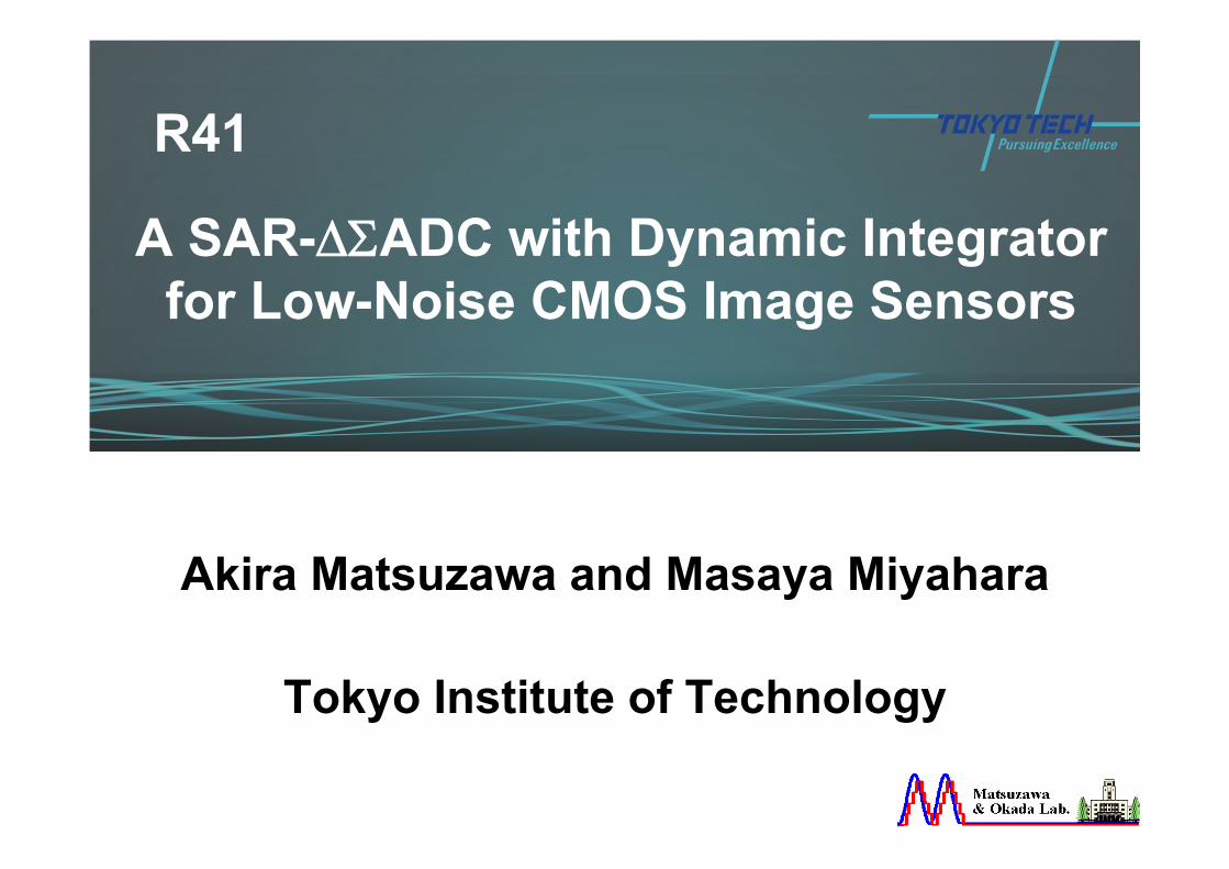
1Contents
• Performance limitation of the SS ADC• General purpose SAR+ΔΣADC• Proposed SAR+ΔΣADC for CIS
– Multiple sampling– CDS and ΔΣ ADC (Avoid Capacitor mismatch)
• Proposed open loop dynamic integrator– Open loop integrator– Dynamic amplifier
• Performance– Simulated– Measured
• SummaryTokyo Tech. A. Matsuzawa
2Attention and apology
• In the proceeding, no simulated data and measured data but only estimated data are used.
• In my presentation, I will use the simulated data and the measured data. The estimated data will not be used, since the noise voltage in my estimation is very optimistic due to neglecting the noise of the integrator.
• I deeply apologize my mistake and your confusion.
Tokyo Tech. A. Matsuzawa
3
1
1
1
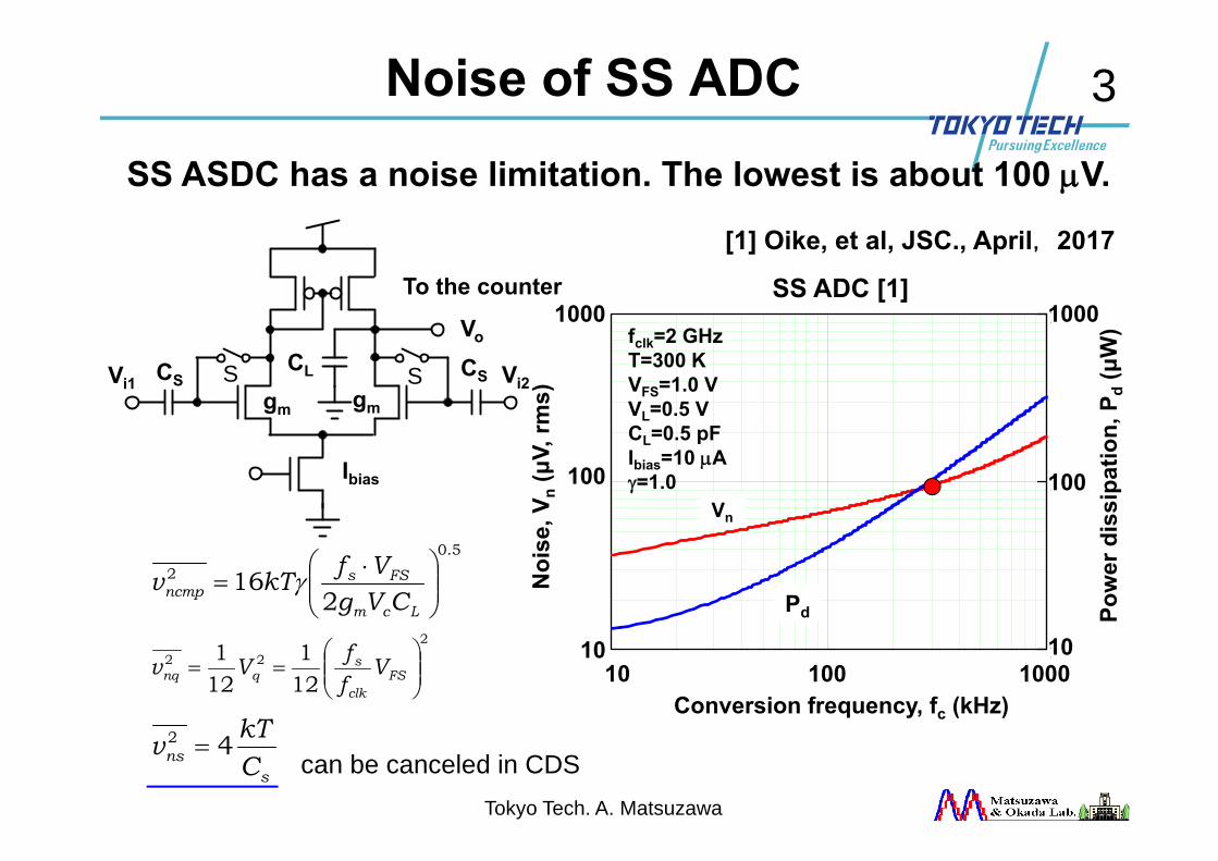
Noise of SS ADC
Tokyo Tech. A. Matsuzawa
Conversion frequency, fc (kHz)
Noi
se, V
n(μ
V, rm
s)
Pow
er d
issi
patio
n, P
d(μ
W)
Pd
fclk=2 GHzT=300 KVFS=1.0 VVL=0.5 VCL=0.5 pFIbias=10 μAγ=1.0
Vn
5.02
216 ⎟⎟
⎠
⎞⎜⎜⎝
⎛ ⋅=
Lcm
FSsncmp CVg
VfkTv γ
sns C
kTv 42 =
222
121
121
⎟⎟⎠
⎞⎜⎜⎝
⎛== FS
clk
sqnq V
ffVv
Vi1 Vi2S SCS CSCL
Vo
Ibias
gm gm
To the counter
can be canceled in CDS
SS ASDC has a noise limitation. The lowest is about 100 μV.
SS ADC [1]
[1] Oike, et al, JSC., April, 2017
1000
100
1010 100 1000
1000
100
10
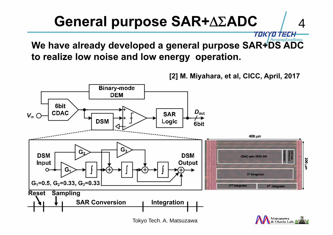
4General purpose SAR+ΔΣADC
Reset SamplingSAR Conversion Integration
We have already developed a general purpose SAR+DS ADCto realize low noise and low energy operation.
[2] M. Miyahara, et al, CICC, April, 2017
Tokyo Tech. A. Matsuzawa
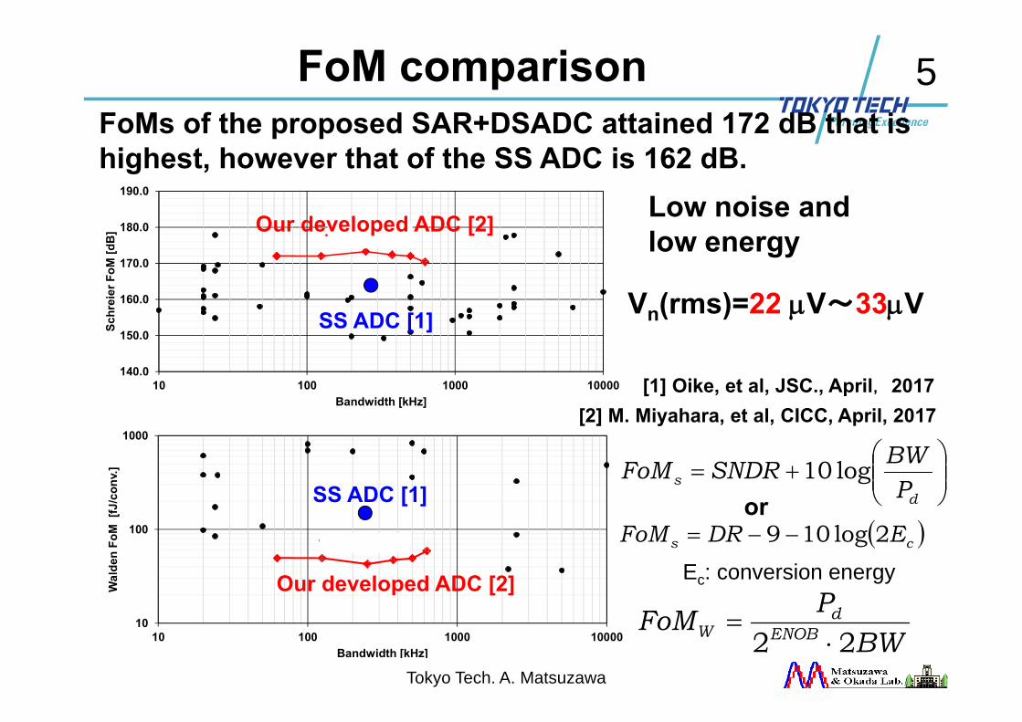
5FoM comparison
Tokyo Tech. A. Matsuzawa
10
100
1000
10 100 1000 10000
Wal
den
FoM
[fJ
/con
v.]
Bandwidth [kHz]
This work
140.0
150.0
160.0
170.0
180.0
190.0
10 100 1000 10000
Schr
eier
FoM
[dB
]
Bandwidth [kHz]
This work
⎟⎟⎠
⎞⎜⎜⎝
⎛+=
ds P
BWSNDRFoM log10
BWPFoM ENOBd
W 22 ⋅=
SS ADC [1]
Our developed ADC [2]
Our developed ADC [2]
SS ADC [1]
[2] M. Miyahara, et al, CICC, April, 2017
FoMs of the proposed SAR+DSADC attained 172 dB that ishighest, however that of the SS ADC is 162 dB.
[1] Oike, et al, JSC., April, 2017
Vn(rms)=22 μV~33μV
Low noise and low energy
( )cs EDRFoM 2log109 −−=or
Ec: conversion energy
6
∫ ∫
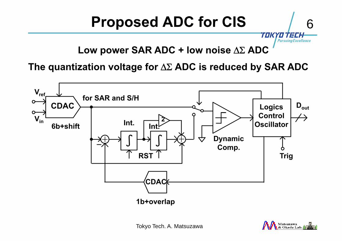
Proposed ADC for CIS
Tokyo Tech. A. Matsuzawa
CDAC
6b+shift
CDAC
Int. Int.
RST
DynamicComp.
Vin
Vref
Trig
LogicsControl
Oscillator
Dout
2
for SAR and S/H
Low power SAR ADC + low noise ΔΣ ADCThe quantization voltage for ΔΣ ADC is reduced by SAR ADC
1b+overlap
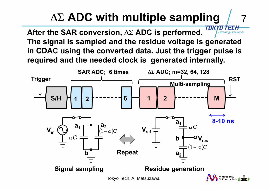
7ΔΣ ADC with multiple sampling
Tokyo Tech. A. Matsuzawa
Vin Vrefa1 a2
b
b
a1
a2
Cα( )Cα−1
( )Cα−1
Cα
Repeat
Vres
Signal sampling Residue generation
S/H 1 2 6 1 2 M
SAR ADC; 6 times ΔΣ ADC; m=32, 64, 128
Multi-samplingTrigger RST
After the SAR conversion, ΔΣ ADC is performed.The signal is sampled and the residue voltage is generated in CDAC using the converted data. Just the trigger pulse is required and the needed clock is generated internally.
8-10 ns
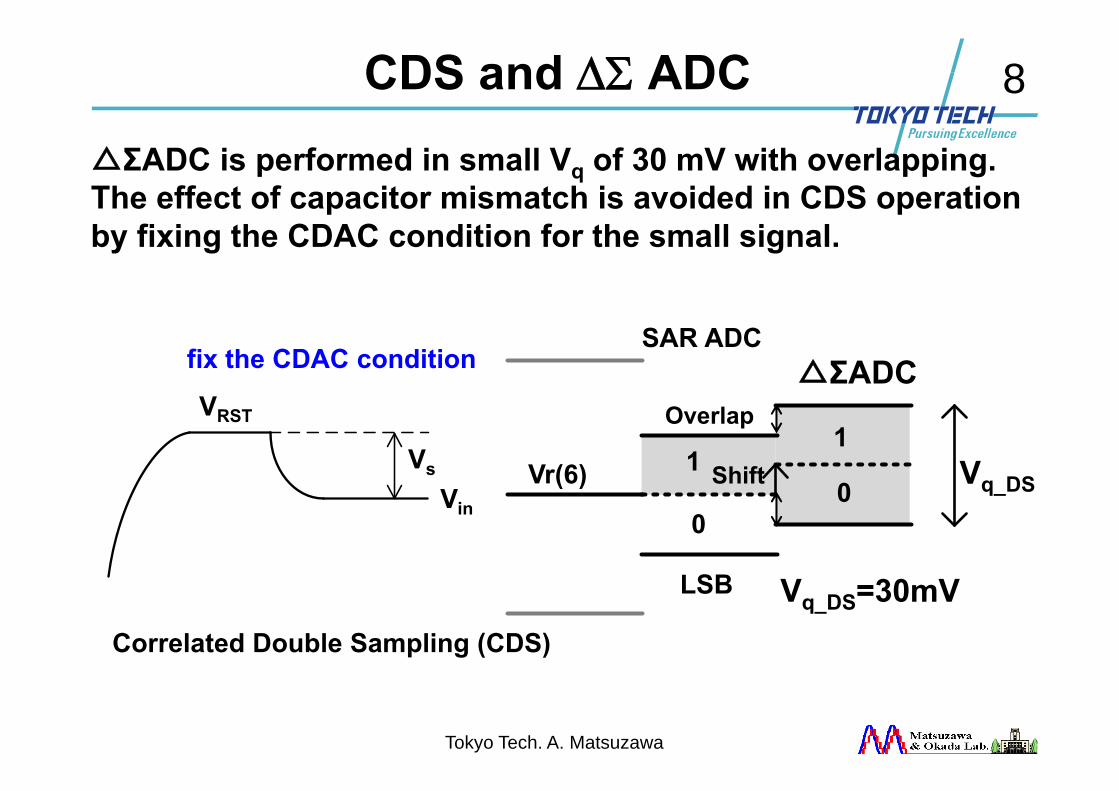
8CDS and ΔΣ ADC
Tokyo Tech. A. Matsuzawa
1
01
0
Vr(6) Vq_DS
VRST
Vin
Vs
LSB
Shift
△ΣADCOverlap
Correlated Double Sampling (CDS)
SAR ADC
Vq_DS=30mV
△ΣADC is performed in small Vq of 30 mV with overlapping.The effect of capacitor mismatch is avoided in CDS operationby fixing the CDAC condition for the small signal.
fix the CDAC condition
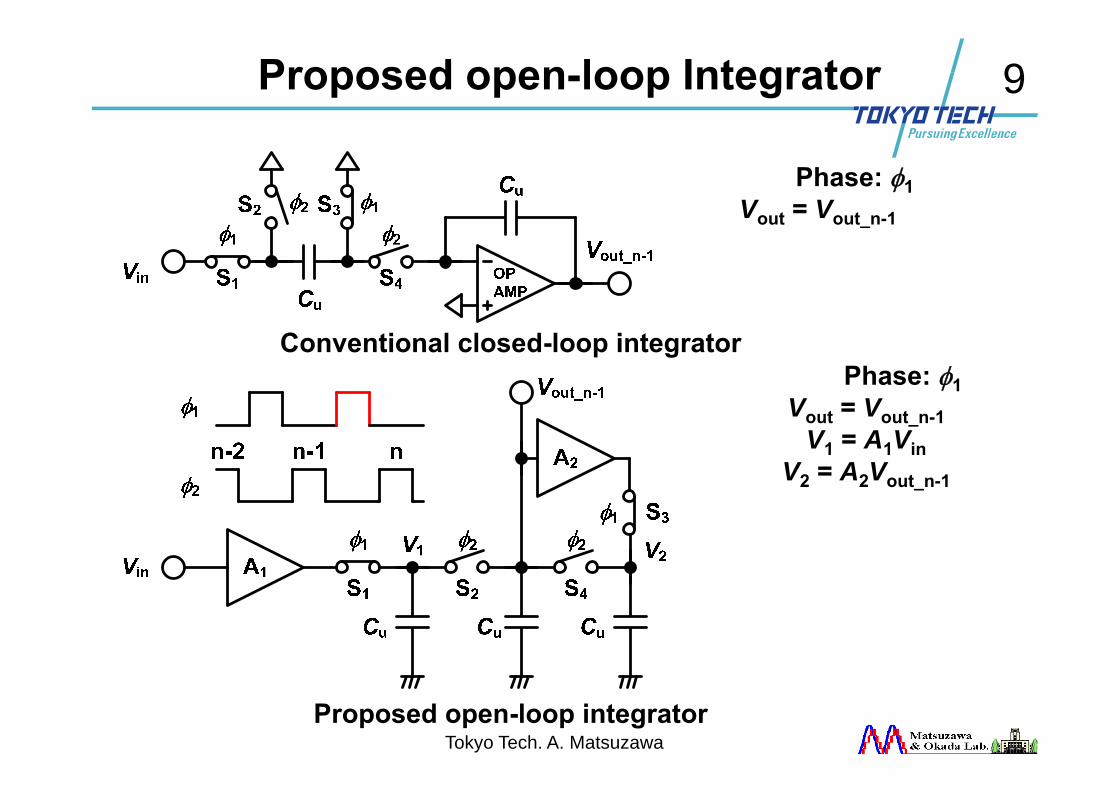
9Proposed open-loop Integrator
Phase: φ1Vout = Vout_n-1
Phase: φ1Vout = Vout_n-1
V1 = A1VinV2 = A2Vout_n-1
Tokyo Tech. A. Matsuzawa
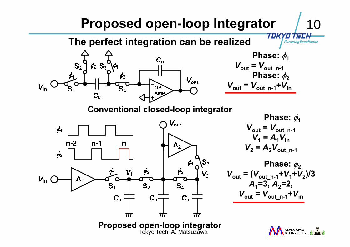
10Proposed open-loop Integrator
Phase: φ1Vout = Vout_n-1
Phase: φ2Vout = Vout_n-1+Vin
Phase: φ1Vout = Vout_n-1
V1 = A1VinV2 = A2Vout_n-1
Phase: φ2Vout = (Vout_n-1+V1+V2)/3
A1=3, A2=2,Vout = Vout_n-1+Vin
The perfect integration can be realized
Tokyo Tech. A. Matsuzawa
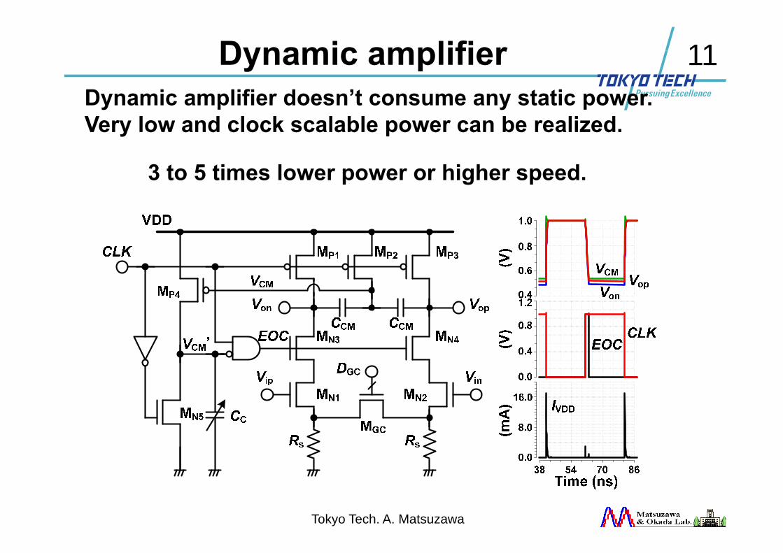
11Dynamic amplifier
Tokyo Tech. A. Matsuzawa
Dynamic amplifier doesn’t consume any static power.Very low and clock scalable power can be realized.
3 to 5 times lower power or higher speed.
12
0
0
3
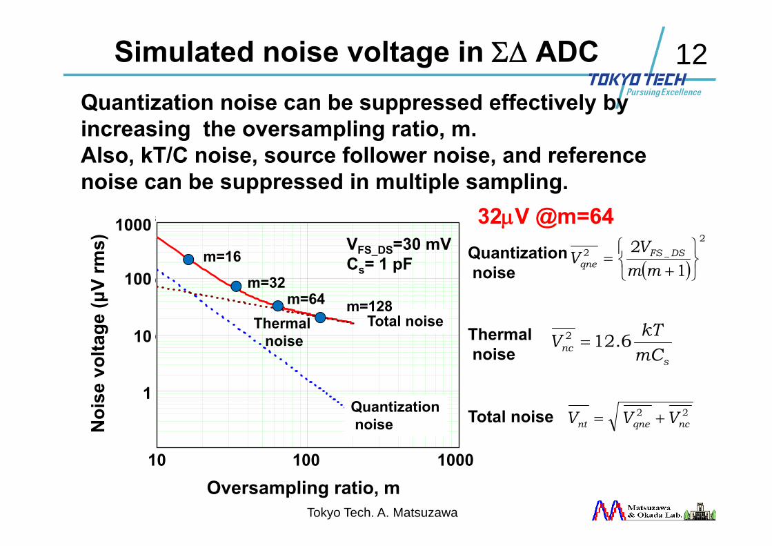
Simulated noise voltage in ΣΔ ADC
Tokyo Tech. A. Matsuzawa
Total noise
Quantizationnoise
Oversampling ratio, m
Thermalnoise
Noi
se v
olta
ge (μ
Vrm
s)
m=16
m=32m=64 m=128
VFS_DS=30 mVCs= 1 pF ( )
2_2
12
⎭⎬⎫
⎩⎨⎧
+=
mmV
V DSFSqne
snc mC
kTV 6.122 =
22ncqnent VVV +=
Quantization noise can be suppressed effectively byincreasing the oversampling ratio, m.Also, kT/C noise, source follower noise, and reference noise can be suppressed in multiple sampling.
Total noise
Thermalnoise
Quantizationnoise
32μV @m=641000
100
10
10 100 1000
1
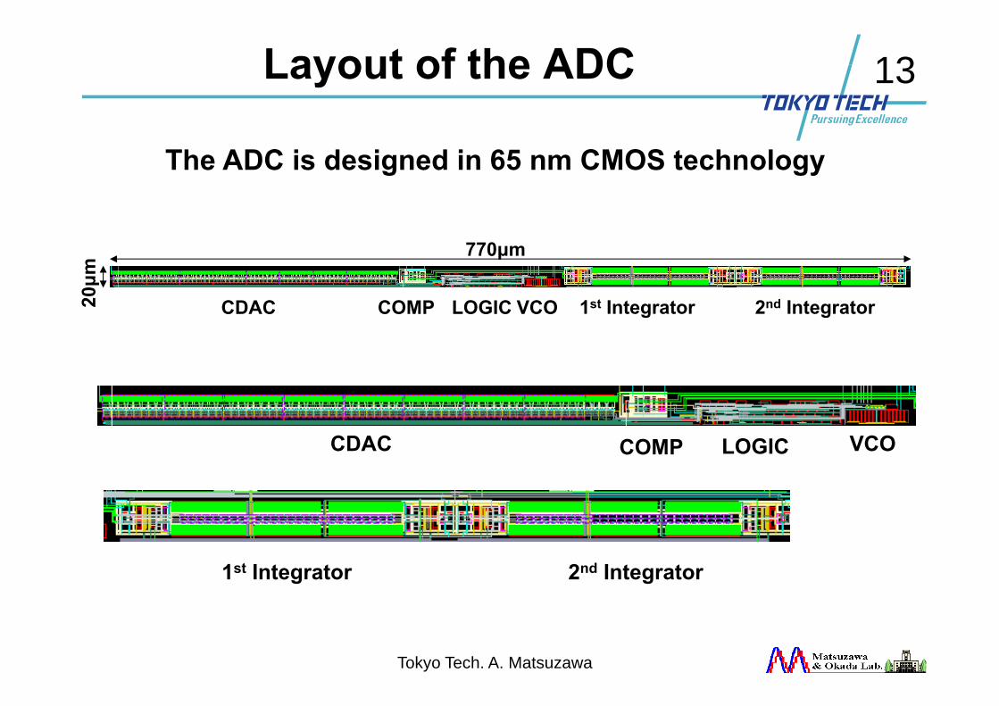
13Layout of the ADC20μm
770μm
CDAC COMP LOGIC VCO 1st Integrator 2nd Integrator
Tokyo Tech. A. Matsuzawa
The ADC is designed in 65 nm CMOS technology
CDAC COMP LOGIC VCO
1st Integrator 2nd Integrator
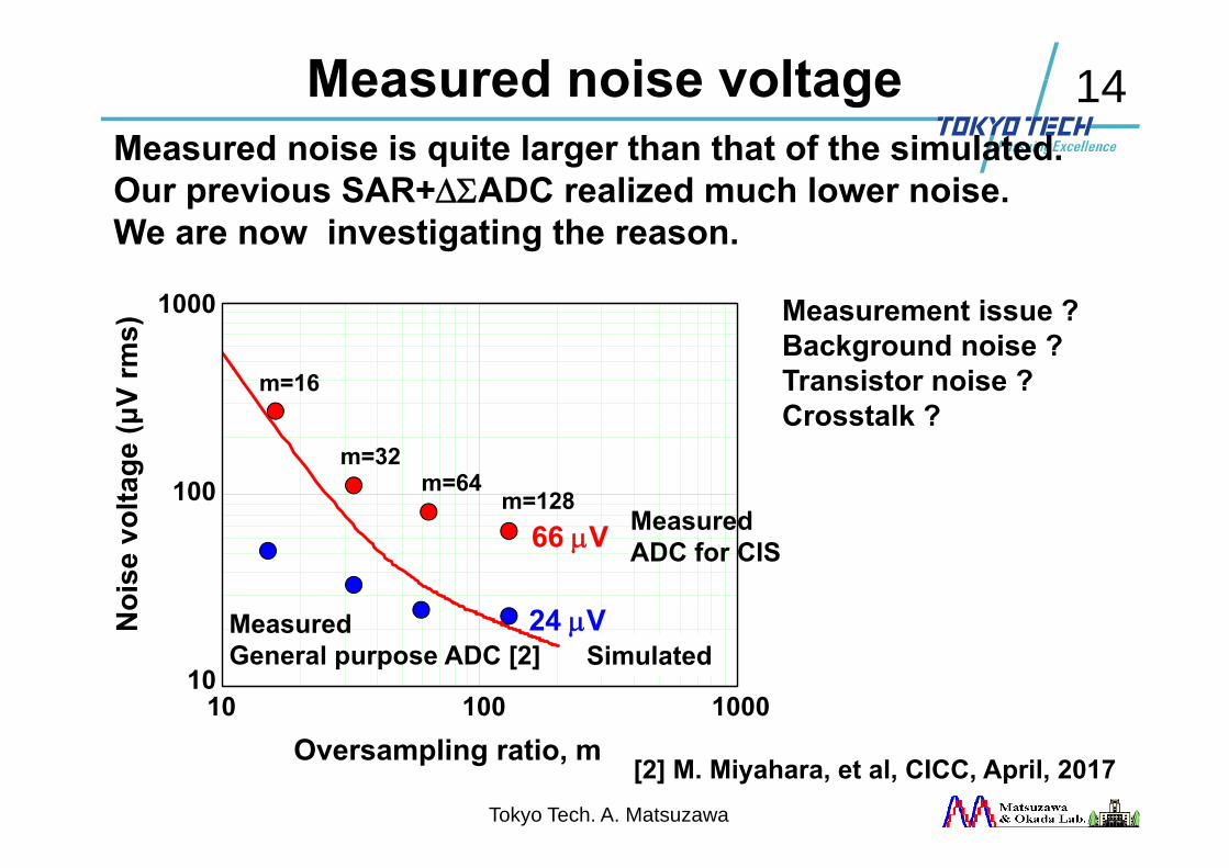
14Measured noise voltage
Tokyo Tech. A. Matsuzawa
MeasuredADC for CIS
SimulatedMeasuredGeneral purpose ADC [2]
[2] M. Miyahara, et al, CICC, April, 2017
Measured noise is quite larger than that of the simulated. Our previous SAR+ΔΣADC realized much lower noise.We are now investigating the reason.
66 μV
24 μV
Measurement issue ?Background noise ?Transistor noise ?Crosstalk ?
Oversampling ratio, m
Noi
se v
olta
ge (μ
Vrm
s)
m=16
m=32m=64
m=128
1000
100
1010 100 1000
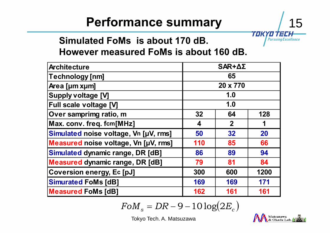
15Performance summary
Tokyo Tech. A. Matsuzawa
( )cs EDRFoM 2log109 −−=
Simulated FoMs is about 170 dB.However measured FoMs is about 160 dB.
ArchitectureTechnology [nm]Area [μm xμm]Supply voltage [V]Full scale voltage [V]Over samprimg ratio, m 32 64 128Max. conv. freq. fcm[MHz] 4 2 1Simulated noise voltage, Vn [μV, rms] 50 32 20Measured noise voltage, Vn [μV, rms] 110 85 66Simulated dynamic range, DR [dB] 86 89 94Measured dynamic range, DR [dB] 79 81 84Coversion energy, Ec [pJ] 300 600 1200Simurated FoMs [dB] 169 169 171Measured FoMs [dB] 162 161 161
SAR+∆Σ65
20 x 7701.01.0
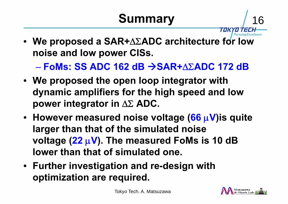
16Summary
• We proposed a SAR+ΔΣADC architecture for low noise and low power CISs.– FoMs: SS ADC 162 dB SAR+ΔΣADC 172 dB
• We proposed the open loop integrator with dynamic amplifiers for the high speed and low power integrator in ΔΣ ADC.
• However measured noise voltage (66 μV)is quite larger than that of the simulated noisevoltage (22 μV). The measured FoMs is 10 dB lower than that of simulated one.
• Further investigation and re-design with optimization are required.
Tokyo Tech. A. Matsuzawa
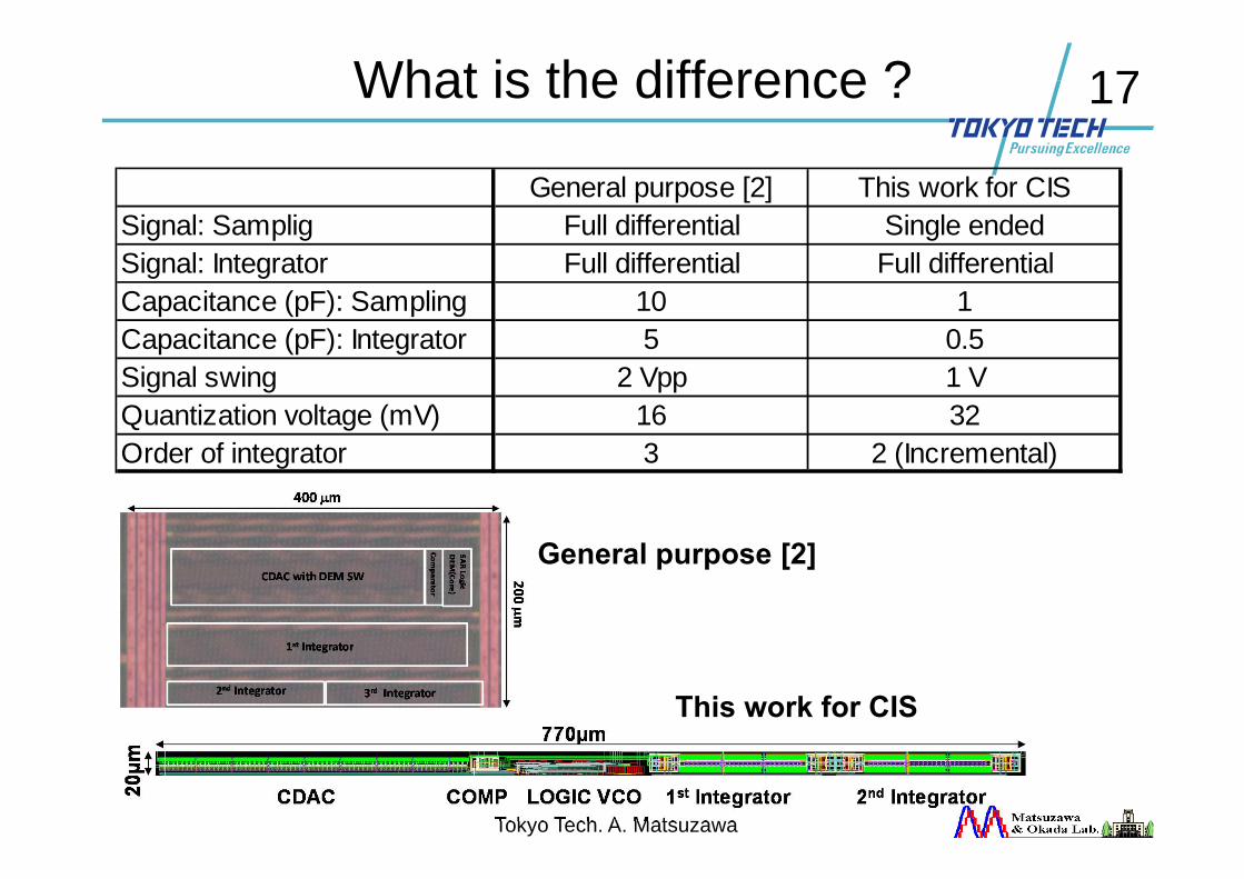
17What is the difference ?
Tokyo Tech. A. Matsuzawa
General purpose [2]
This work for CIS
General purpose [2] This work for CISSignal: Samplig Full differential Single endedSignal: Integrator Full differential Full differentialCapacitance (pF): Sampling 10 1Capacitance (pF): Integrator 5 0.5Signal swing 2 Vpp 1 VQuantization voltage (mV) 16 32Order of integrator 3 2 (Incremental)