Optimize Your SAR ADC Design - Texas...
44
1 Optimize Your SAR ADC Design Bonnie Baker Senior Applications Engineer [email protected] Special Thanks for Inputs from Tim Green Rick Downs Miro Oljaca The most popular and versatile Analog-to-Digital Converter (ADC) has a Successive Approximation Register (SAR) topology. These converters work by comparing an analog voltage signal to known fractions of the full-scale input voltage and then setting or clearing bits in the ADC’s data register. Modern SAR converters use a Capacitive Data Acquisition Converter (C-DAC) to successively compare bit combinations. Usually these devices have an integrated sample/hold input function. It is common to use an operational amplifier (Op Amp) to directly drive the input of a SAR Analog-to-digital converter (SAR-ADC). Although this configuration is an acceptable practice in manufacturer’s data sheets, it has the potential to create circuit performance limitations. For optimum performance, C-DAC SAR-ADCs require the correct front-end buffer and filter. The additional input filter or RC- network will relax the driving Op Amp requirements. This presentation details the reasons for an input filter and buffer amplifier to the C-DAC SAR-ADC along with an analytical approach to selecting the filter components and op amp characteristics.
Transcript of Optimize Your SAR ADC Design - Texas...
1
Optimize Your SAR ADC Design
Bonnie BakerSenior Applications Engineer
[email protected] Special Thanks for Inputs fromTim Green
Rick DownsMiro Oljaca
The most popular and versatile Analog-to-Digital Converter (ADC) has a Successive Approximation Register (SAR) topology. These converters work by comparing an analog voltage signal to known fractions of the full-scale input voltage and then setting or clearing bits in the ADC’s data register. Modern SAR converters use a Capacitive Data Acquisition Converter (C-DAC) to successively compare bit combinations. Usually these devices have an integrated sample/hold input function. It is common to use an operational amplifier (Op Amp) to directly drive the input of a SAR Analog-to-digital converter (SAR-ADC). Although this configuration is an acceptable practice in manufacturer’s data sheets, it has the potential to create circuit performance limitations. For optimum performance, C-DAC SAR-ADCs require the correct front-end buffer and filter. The additional input filter or RC-network will relax the driving Op Amp requirements. This presentation details the reasons for an input filter and buffer amplifier to the C-DAC SAR-ADC along with an analytical approach to selecting the filter components and op amp characteristics.
2
SAR ADC System Design
OpAmpSignal Bandwidth
Slew Rate
Output Impedance
+
-
VS
A/DOp AmpFilter
DOUT
FilterCharge Reservoir
Capacitor Load Isolation
Noise Filtering
ADCAcquisition Time
Data Rate
Resolution
ADC Input Topology
ADC Ref In
SAR
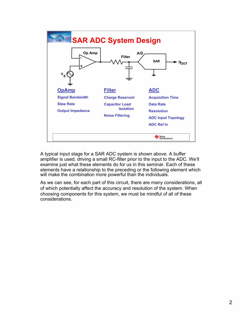
A typical input stage for a SAR ADC system is shown above. A buffer amplifier is used, driving a small RC-filter prior to the input to the ADC. We’ll examine just what these elements do for us in this seminar. Each of these elements have a relationship to the preceding or the following element which will make the combination more powerful than the individuals.
As we can see, for each part of this circuit, there are many considerations, all of which potentially affect the accuracy and resolution of the system. When choosing components for this system, we must be mindful of all of these considerations.

3
The Design Tools We Will Use
• Data Sheet Parameters .
• Rules of Thumb .
• Tricks and Tips .
• Testing .
Many articles have been written about choosing op amps for use in driving ADCs (see last page of this presentation). All of the articles point out things that we should watch out for. From these articles and this seminar, we will observe some guidelines and make it easier and faster to get to a good design.
The design procedure we will present contains some rigorous analysis, but also observes rules of thumb, some “tricks”, and of course refers to the datasheets of the products in our circuit. As always with analog circuitry and proof of function will be required with some testing and prototyping.
4
Design Procedure
+
-
VS
A/DOp AmpFilter
RFLTCFLT
+VCC +VREF
DOUT
A
Signal (1)BandwidthFull-scale
Range
?
E
Op amp (5)Input StageBandwidthOutput ROSettling Time
?
C
?
D
RC pair (3,4)ADC vs capCap qualityOpa vs Resistor
?
B
ADC (2)Full-scale input rangeAcquisition timeKick Back Voltage &
Charge
0 V
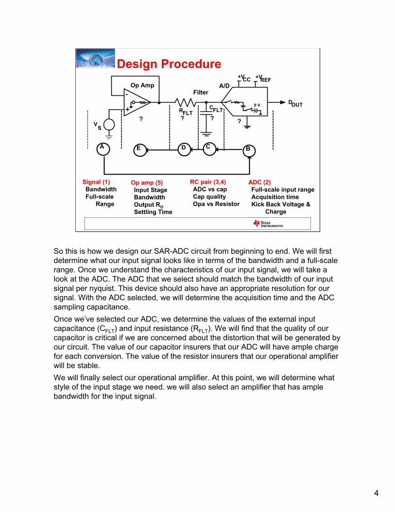
So this is how we design our SAR-ADC circuit from beginning to end. We will first determine what our input signal looks like in terms of the bandwidth and a full-scale range. Once we understand the characteristics of our input signal, we will take a look at the ADC. The ADC that we select should match the bandwidth of our input signal per nyquist. This device should also have an appropriate resolution for our signal. With the ADC selected, we will determine the acquisition time and the ADC sampling capacitance. Once we’ve selected our ADC, we determine the values of the external input capacitance (CFLT) and input resistance (RFLT). We will find that the quality of our capacitor is critical if we are concerned about the distortion that will be generated by our circuit. The value of our capacitor insurers that our ADC will have ample charge for each conversion. The value of the resistor insurers that our operational amplifier will be stable. We will finally select our operational amplifier. At this point, we will determine what style of the input stage we need. we will also select an amplifier that has ample bandwidth for the input signal.
5
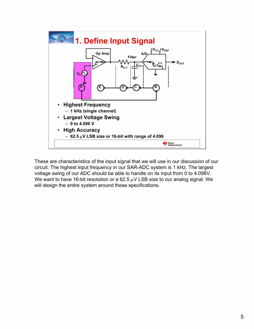
1. Define Input Signal
• Highest Frequency– 1 kHz (single channel)
• Largest Voltage Swing– 0 to 4.096 V
• High Accuracy– 62.5 μV LSB size or 16-bit with range of 4.096
+
-
VS
A/DOp AmpFilter
RFLTCFLT
+VCC +VREF
DOUT
A E CD B
0 V
These are characteristics of the input signal that we will use in our discussion of our circuit. The highest input frequency in our SAR-ADC system is 1 kHz. The largest voltage swing of our ADC should be able to handle on its input from 0 to 4.096V. We want to have 16-bit resolution or a 62.5 μV LSB size to our analog signal. We will design the entire system around these specifications.
6
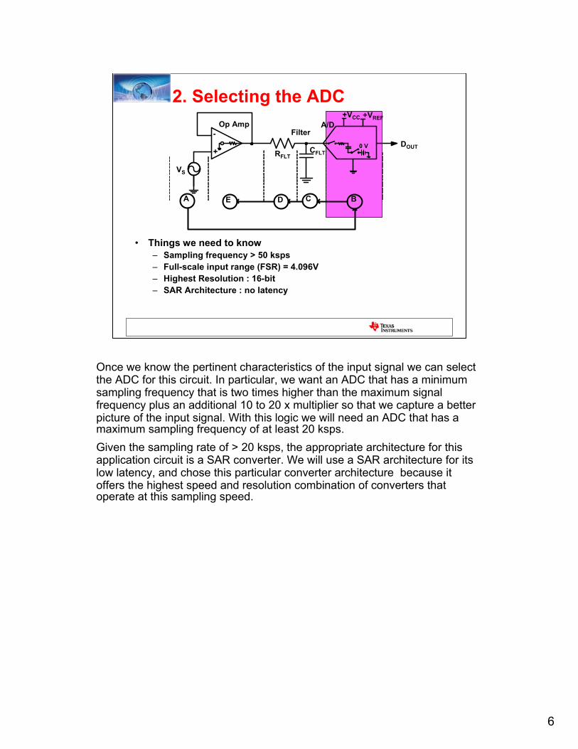
2. Selecting the ADC
• Things we need to know– Sampling frequency > 50 ksps– Full-scale input range (FSR) = 4.096V– Highest Resolution : 16-bit– SAR Architecture : no latency
+
-
VS
A/DOp AmpFilter
RFLTCFLT
+VCC +VREF
DOUT
A E CD B
0 V
Once we know the pertinent characteristics of the input signal we can select the ADC for this circuit. In particular, we want an ADC that has a minimum sampling frequency that is two times higher than the maximum signal frequency plus an additional 10 to 20 x multiplier so that we capture a better picture of the input signal. With this logic we will need an ADC that has a maximum sampling frequency of at least 20 ksps. Given the sampling rate of > 20 ksps, the appropriate architecture for this application circuit is a SAR converter. We will use a SAR architecture for its low latency, and chose this particular converter architecture because it offers the highest speed and resolution combination of converters that operate at this sampling speed.
7
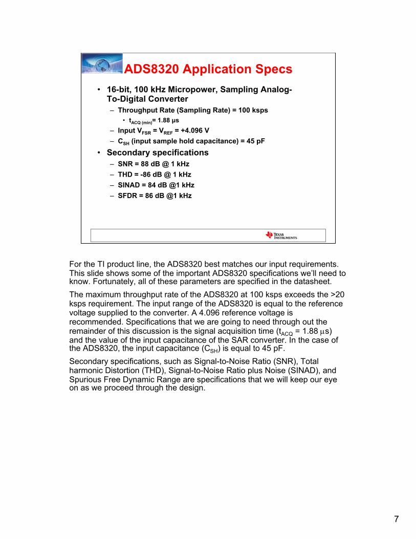
ADS8320 Application Specs• 16-bit, 100 kHz Micropower, Sampling Analog-
To-Digital Converter– Throughput Rate (Sampling Rate) = 100 ksps
• tACQ (min)= 1.88 μs– Input VFSR = VREF = +4.096 V– CSH (input sample hold capacitance) = 45 pF
• Secondary specifications– SNR = 88 dB @ 1 kHz– THD = -86 dB @ 1 kHz– SINAD = 84 dB @1 kHz– SFDR = 86 dB @1 kHz
For the TI product line, the ADS8320 best matches our input requirements. This slide shows some of the important ADS8320 specifications we’ll need to know. Fortunately, all of these parameters are specified in the datasheet.The maximum throughput rate of the ADS8320 at 100 ksps exceeds the >20 ksps requirement. The input range of the ADS8320 is equal to the reference voltage supplied to the converter. A 4.096 reference voltage is recommended. Specifications that we are going to need through out the remainder of this discussion is the signal acquisition time (tACQ = 1.88 μs) and the value of the input capacitance of the SAR converter. In the case of the ADS8320, the input capacitance (CSH) is equal to 45 pF.Secondary specifications, such as Signal-to-Noise Ratio (SNR), Total harmonic Distortion (THD), Signal-to-Noise Ratio plus Noise (SINAD), and Spurious Free Dynamic Range are specifications that we will keep our eye on as we proceed through the design.
8
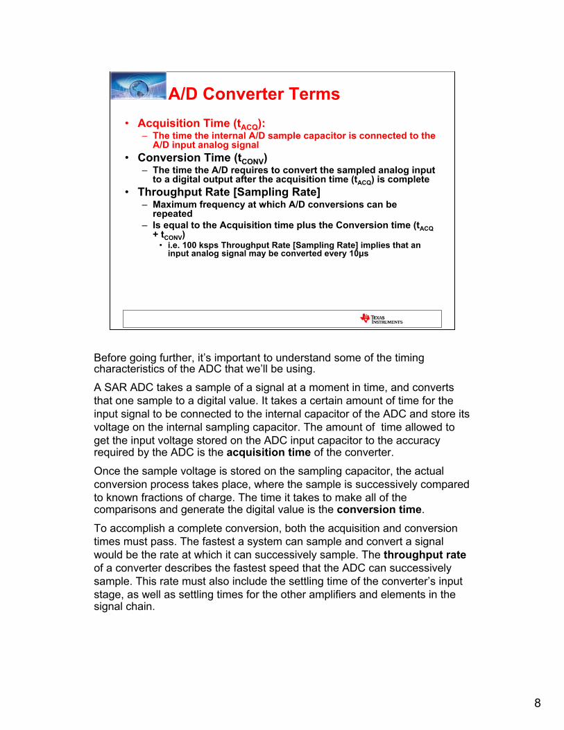
A/D Converter Terms• Acquisition Time (tACQ):
– The time the internal A/D sample capacitor is connected to the A/D input analog signal
• Conversion Time (tCONV)– The time the A/D requires to convert the sampled analog input
to a digital output after the acquisition time (tACQ) is complete• Throughput Rate [Sampling Rate]
– Maximum frequency at which A/D conversions can be repeated
– Is equal to the Acquisition time plus the Conversion time (tACQ+ tCONV)
• i.e. 100 ksps Throughput Rate [Sampling Rate] implies that an input analog signal may be converted every 10μs
Before going further, it’s important to understand some of the timing characteristics of the ADC that we’ll be using.
A SAR ADC takes a sample of a signal at a moment in time, and converts that one sample to a digital value. It takes a certain amount of time for the input signal to be connected to the internal capacitor of the ADC and store its voltage on the internal sampling capacitor. The amount of time allowed to get the input voltage stored on the ADC input capacitor to the accuracy required by the ADC is the acquisition time of the converter.
Once the sample voltage is stored on the sampling capacitor, the actual conversion process takes place, where the sample is successively compared to known fractions of charge. The time it takes to make all of the comparisons and generate the digital value is the conversion time.
To accomplish a complete conversion, both the acquisition and conversion times must pass. The fastest a system can sample and convert a signal would be the rate at which it can successively sample. The throughput rateof a converter describes the fastest speed that the ADC can successively sample. This rate must also include the settling time of the converter’s input stage, as well as settling times for the other amplifiers and elements in the signal chain.
9
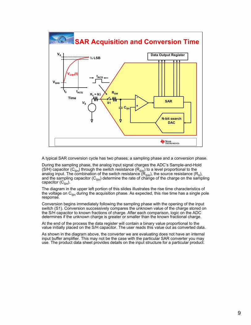
SAR Acquisition and Conversion TimeVS
VSH0
½ LSB
Time
tACQt0
VCSH(t)
CSH
VS
N-bit searchDAC
SAR+
-
Data Output Register
RSW
tACQ
RS = 0Ω
S1
A typical SAR conversion cycle has two phases; a sampling phase and a conversion phase.During the sampling phase, the analog input signal charges the ADC’s Sample-and-Hold (S/H) capacitor (CSH) through the switch resistance (RSW) to a level proportional to the analog input. The combination of the switch resistance (RSW), the source resistance (RS), and the sampling capacitor (CSH) determine the rate of change of the charge on the sampling capacitor (CSH).The diagram in the upper left portion of this slides illustrates the rise time characteristics of the voltage on CSH during the acquisition phase. As expected, this rise time has a single pole response. Conversion begins immediately following the sampling phase with the opening of the input switch (S1). Conversion successively compares the unknown value of the charge stored on the S/H capacitor to known fractions of charge. After each comparison, logic on the ADC determines if the unknown charge is greater or smaller than the known fractional charge. At the end of the process the data register will contain a binary value proportional to the value initially placed on the S/H capacitor. The user reads this value out as converted data.As shown in the diagram above, the converter we are evaluating does not have an internal input buffer amplifier. This may not be the case with the particular SAR converter you may use. The product data sheet provides details on the input structure for a particular product.
10
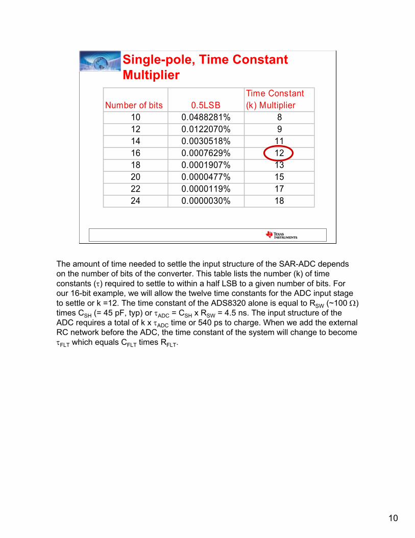
Single-pole, Time Constant Multiplier
Number of bits 0.5LSBTime Constant (k) Multiplier
10 0.0488281% 812 0.0122070% 914 0.0030518% 1116 0.0007629% 1218 0.0001907% 1320 0.0000477% 1522 0.0000119% 1724 0.0000030% 18
The amount of time needed to settle the input structure of the SAR-ADC depends on the number of bits of the converter. This table lists the number (k) of time constants (τ) required to settle to within a half LSB to a given number of bits. For our 16-bit example, we will allow the twelve time constants for the ADC input stage to settle or k =12. The time constant of the ADS8320 alone is equal to RSW (~100 Ω) times CSH (= 45 pF, typ) or τADC = CSH x RSW = 4.5 ns. The input structure of the ADC requires a total of k x τADC time or 540 ps to charge. When we add the external RC network before the ADC, the time constant of the system will change to become τFLT which equals CFLT times RFLT.
11
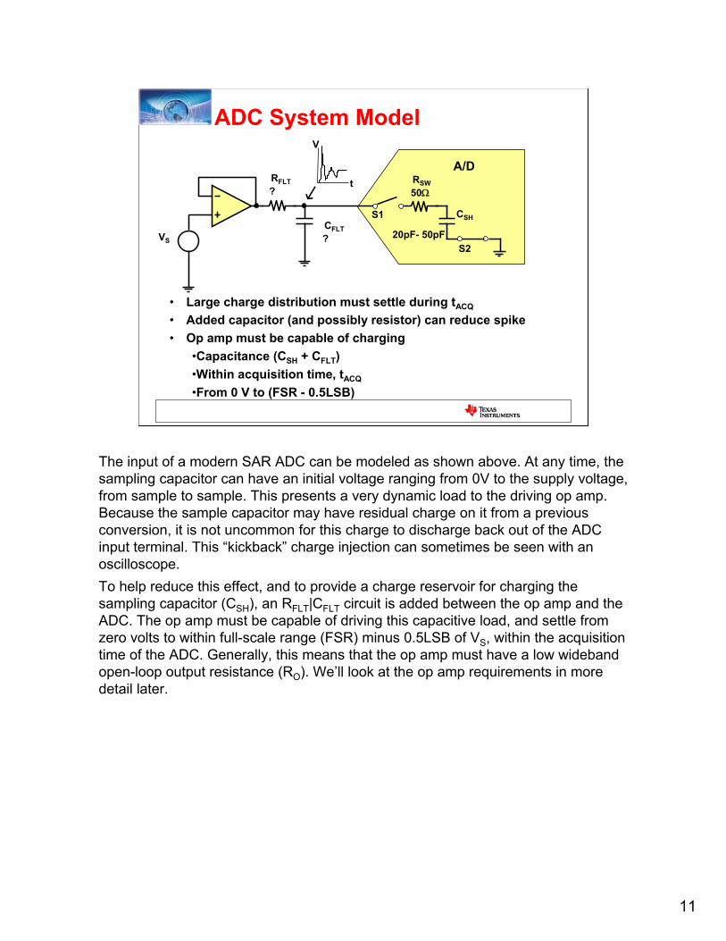
ADC System Model
• Large charge distribution must settle during tACQ
• Added capacitor (and possibly resistor) can reduce spike• Op amp must be capable of charging
•Capacitance (CSH + CFLT) •Within acquisition time, tACQ
•From 0 V to (FSR - 0.5LSB)
RSW
S1
S2
CSH
50Ω
20pF- 50pF
A/DRFLT?
CFLT?
V
t
VS
The input of a modern SAR ADC can be modeled as shown above. At any time, the sampling capacitor can have an initial voltage ranging from 0V to the supply voltage, from sample to sample. This presents a very dynamic load to the driving op amp. Because the sample capacitor may have residual charge on it from a previous conversion, it is not uncommon for this charge to discharge back out of the ADC input terminal. This “kickback” charge injection can sometimes be seen with an oscilloscope.To help reduce this effect, and to provide a charge reservoir for charging the sampling capacitor (CSH), an RFLT|CFLT circuit is added between the op amp and the ADC. The op amp must be capable of driving this capacitive load, and settle from zero volts to within full-scale range (FSR) minus 0.5LSB of VS, within the acquisition time of the ADC. Generally, this means that the op amp must have a low wideband open-loop output resistance (RO). We’ll look at the op amp requirements in more detail later.
12
SAR ADC Input Charge Distribution
• Op amp requirements
– Must charge the ADC cap quickly & accurately
ADS8361
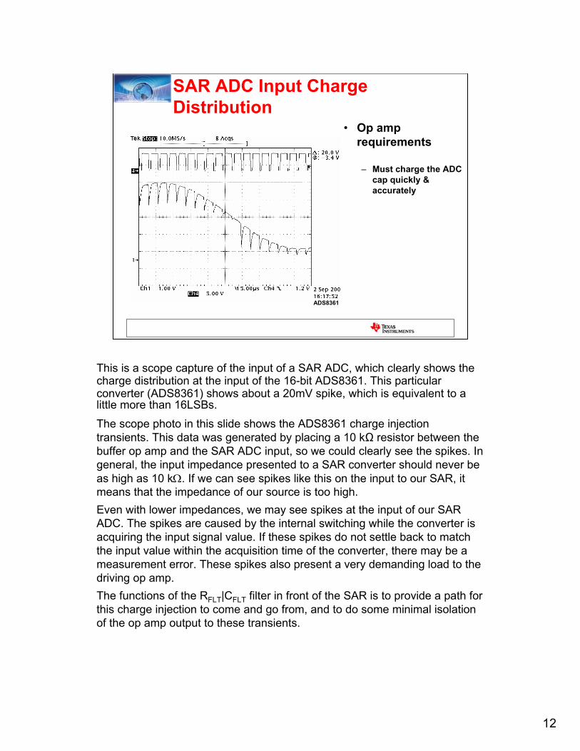
This is a scope capture of the input of a SAR ADC, which clearly shows the charge distribution at the input of the 16-bit ADS8361. This particular converter (ADS8361) shows about a 20mV spike, which is equivalent to a little more than 16LSBs.
The scope photo in this slide shows the ADS8361 charge injectiontransients. This data was generated by placing a 10 kΩ resistor between the buffer op amp and the SAR ADC input, so we could clearly see the spikes. In general, the input impedance presented to a SAR converter should never be as high as 10 kΩ. If we can see spikes like this on the input to our SAR, it means that the impedance of our source is too high.Even with lower impedances, we may see spikes at the input of our SAR ADC. The spikes are caused by the internal switching while the converter is acquiring the input signal value. If these spikes do not settle back to match the input value within the acquisition time of the converter, there may be a measurement error. These spikes also present a very demanding load to the driving op amp. The functions of the RFLT|CFLT filter in front of the SAR is to provide a path for this charge injection to come and go from, and to do some minimal isolation of the op amp output to these transients.
13
ADC Conclusion
• Key ADC specifications per Input Signal– Sampling Rate ≤ 100 ksps– Full-scale input range = 4.096 V
• In following discussion we will use the ADS8320 – tACQ : ADC acquisition time– CSH : ADC input capacitance– k : 16-bit time constant multiplier– VFSR : Full-scale input range of ADC
The converter that we have chosen for our example circuit is the ADS8320. This converter is capable of converting at a 100 ksps rate. The ADS8320 can also operate with a full-scale voltage input range of 4.096V if the reference to the converter, VREF, is equal to 4.096V. As we define the value of the external capacitor, CFLT, we need to know the acquisition time of the converter (tACQ), the ADC input capacitance (CSH), the time constant multiplier for an 16-bit converter (k), and the converter full-scale input voltage range (VFSR).
14
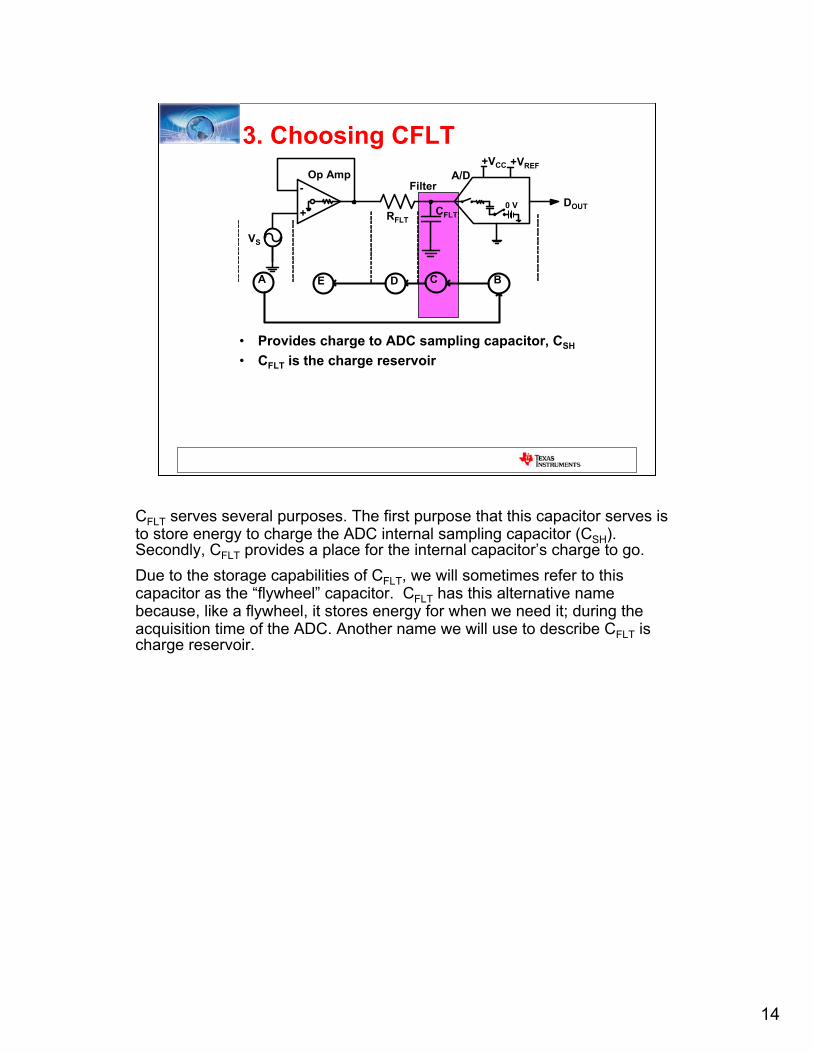
3. Choosing CFLT
• Provides charge to ADC sampling capacitor, CSH
• CFLT is the charge reservoir
+
-
VS
A/DOp AmpFilter
RFLTCFLT
+VCC +VREF
DOUT
A E CD B
0 V
CFLT serves several purposes. The first purpose that this capacitor serves is to store energy to charge the ADC internal sampling capacitor (CSH). Secondly, CFLT provides a place for the internal capacitor’s charge to go. Due to the storage capabilities of CFLT, we will sometimes refer to this capacitor as the “flywheel” capacitor. CFLT has this alternative name because, like a flywheel, it stores energy for when we need it; during the acquisition time of the ADC. Another name we will use to describe CFLT is charge reservoir.
15
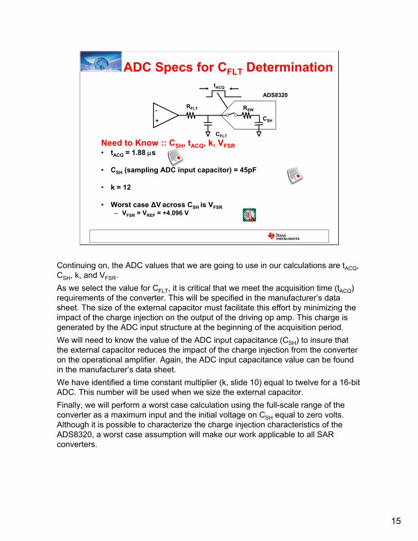
ADC Specs for CFLT Determination
Need to Know :: CSH, tACQ, k, VFSR• tACQ = 1.88 μs
• CSH (sampling ADC input capacitor) = 45pF
• k = 12
• Worst case ΔV across CSH is VFSR – VFSR = VREF = +4.096 V
tACQ
CFLT
RSW
CSH
RFLT
+
-
ADS8320
Continuing on, the ADC values that we are going to use in our calculations are tACQ, CSH, k, and VFSR. As we select the value for CFLT, it is critical that we meet the acquisition time (tACQ) requirements of the converter. This will be specified in the manufacturer’s data sheet. The size of the external capacitor must facilitate this effort by minimizing the impact of the charge injection on the output of the driving op amp. This charge is generated by the ADC input structure at the beginning of the acquisition period. We will need to know the value of the ADC input capacitance (CSH) to insure that the external capacitor reduces the impact of the charge injection from the converter on the operational amplifier. Again, the ADC input capacitance value can be found in the manufacturer’s data sheet. We have identified a time constant multiplier (k, slide 10) equal to twelve for a 16-bit ADC. This number will be used when we size the external capacitor. Finally, we will perform a worst case calculation using the full-scale range of the converter as a maximum input and the initial voltage on CSH equal to zero volts. Although it is possible to characterize the charge injection characteristics of the ADS8320, a worst case assumption will make our work applicable to all SAR converters.
16
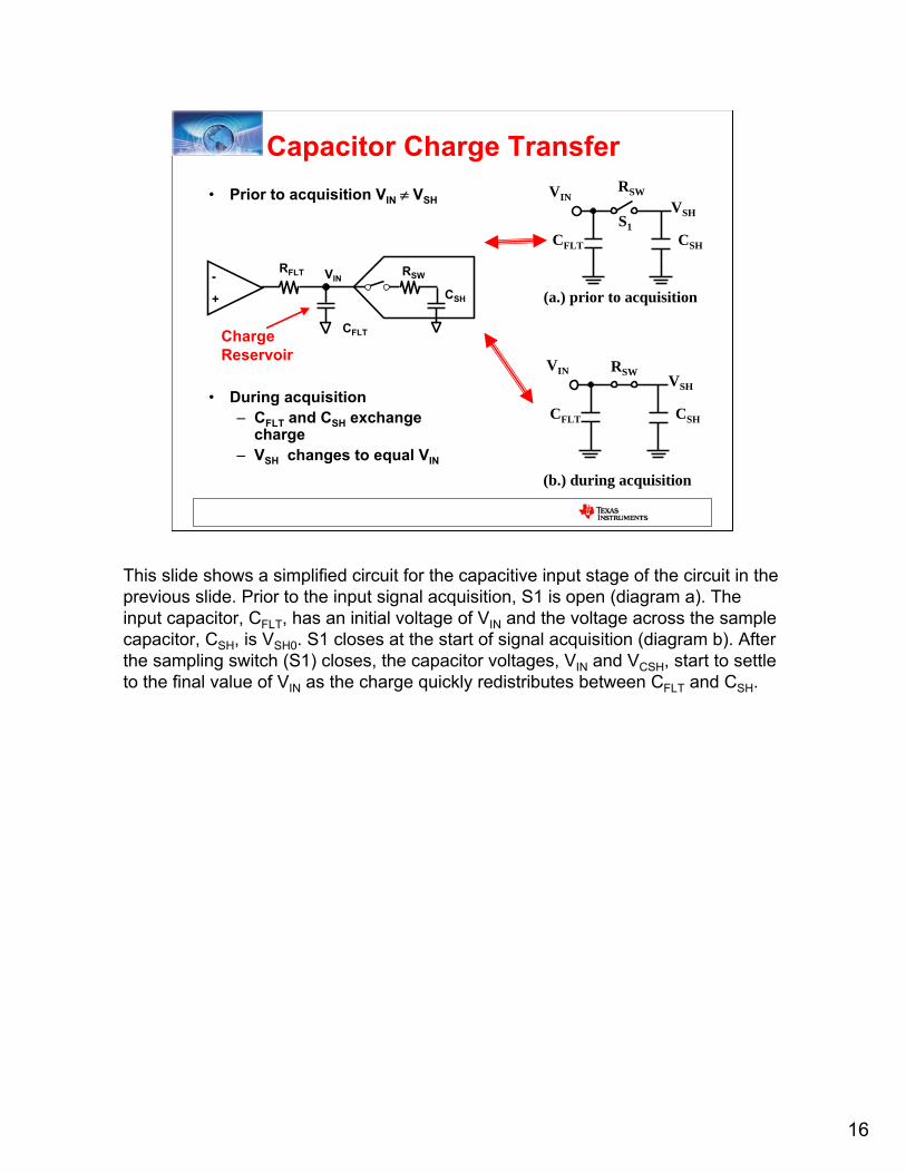
Capacitor Charge Transfer• Prior to acquisition VIN ≠ VSH
• During acquisition – CFLT and CSH exchange
charge– VSH changes to equal VIN
VIN
CFLT CSH
RSW
VSH
(a.) prior to acquisition
S1
VIN
CFLT CSH
RSWVSH
(b.) during acquisition
CFLT
RSW
CSH
RFLT
+
-
ChargeReservoir
VIN
This slide shows a simplified circuit for the capacitive input stage of the circuit in the previous slide. Prior to the input signal acquisition, S1 is open (diagram a). The input capacitor, CFLT, has an initial voltage of VIN and the voltage across the sample capacitor, CSH, is VSH0. S1 closes at the start of signal acquisition (diagram b). After the sampling switch (S1) closes, the capacitor voltages, VIN and VCSH, start to settle to the final value of VIN as the charge quickly redistributes between CFLT and CSH.
17
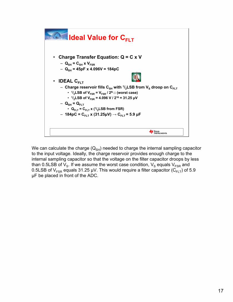
Ideal Value for CFLT
• Charge Transfer Equation: Q = C x V– QSH = CSH x VFSR
– QSH = 45pF x 4.096V = 184pC
• IDEAL CFLT– Charge reservoir fills CSH with 1/2LSB from VS droop on CFLT
• 1/2LSB of VFSR = VFSR / 2N :: (worst case)• 1/2LSB of VFSR = 4.096 V / 216 = 31.25 μV
– QSH = QFLT• QFLT = CFLT x (1/2LSB from FSR)
– 184pC = CFLT x (31.25μV) → CFLT = 5.9 μF
We can calculate the charge (QSH) needed to charge the internal sampling capacitor to the input voltage. Ideally, the charge reservoir provides enough charge to the internal sampling capacitor so that the voltage on the filter capacitor droops by less than 0.5LSB of VS. If we assume the worst case condition, VS equals VFSR and 0.5LSB of VFSR equals 31.25 µV. This would require a filter capacitor (CFLT) of 5.9 µF be placed in front of the ADC.
18
IDEAL CFLT = 5.9 μF: Assessment
• The Driving Op Amp probably – Can not directly drive a 5.9 mF capacitor– Circuit may be marginally stable – Could have transient current problems
• With resistor between Op Amp and capacitor– Resistor and capacitor still need to meet signal
bandwidth– Resistor may not be large enough to help isolate
CFLT
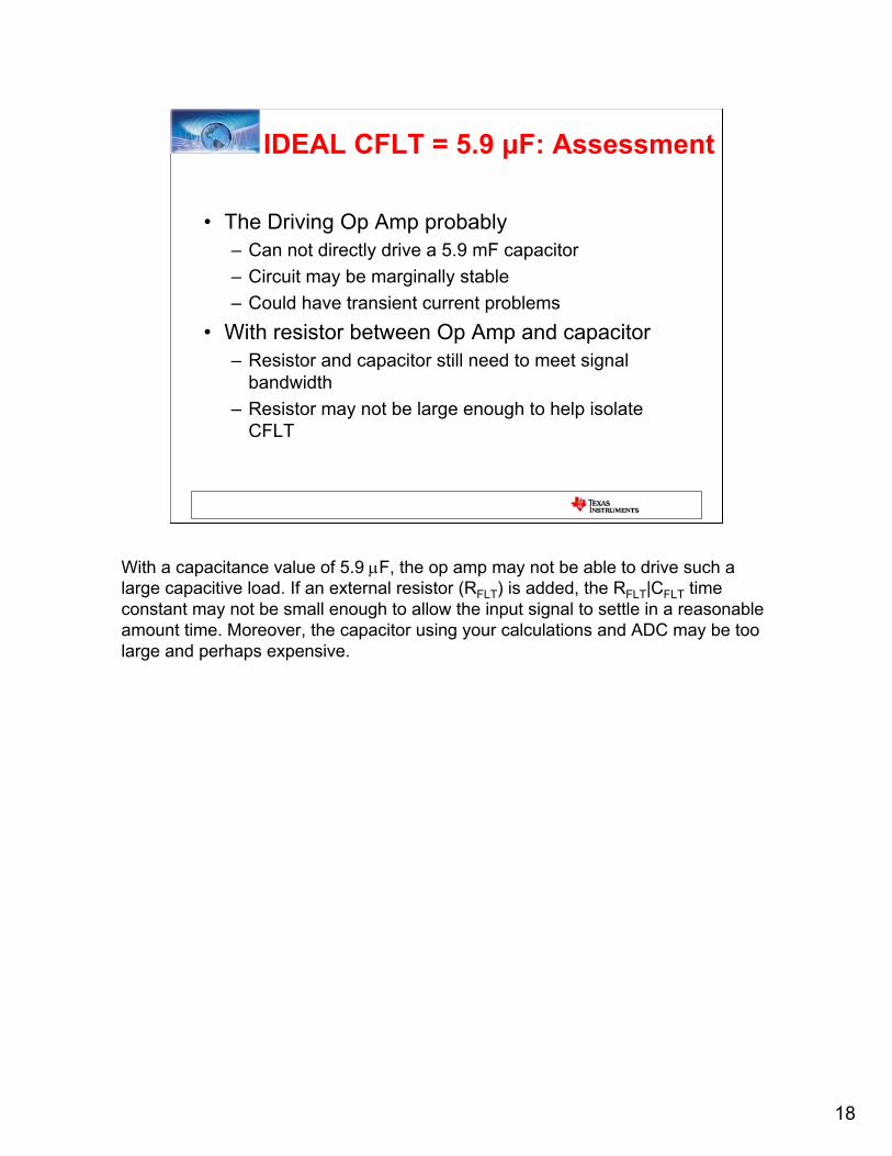
With a capacitance value of 5.9 μF, the op amp may not be able to drive such a large capacitive load. If an external resistor (RFLT) is added, the RFLT|CFLT time constant may not be small enough to allow the input signal to settle in a reasonable amount time. Moreover, the capacitor using your calculations and ADC may be too large and perhaps expensive.
19
CFLT Suggested Modification• Starting Point :: Partition the charge reservoir
– 95% from CFLT– 5% from Op Amp
• CFLT value provides QSH with <5% droop on CFLT– QFLT = QSH– QFLT = CFLT x (0.05 VFSR)– 184pC = CFLT x (0.05 x 4.096V) → CFLT = 898 pF– We’ll use 1000pF or 1 nF
• Ensure CFLT ≥ 20 x CSH– During tACQ the Op Amp must be able to replace 5% VFSR on CFLT
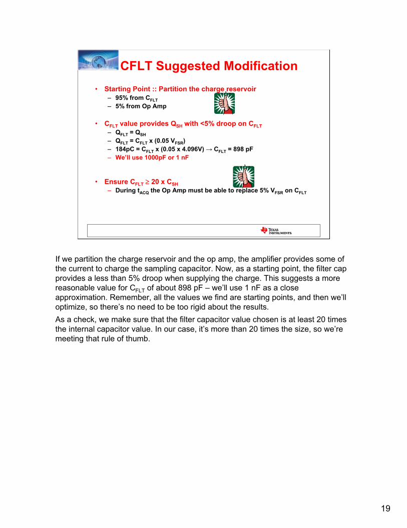
If we partition the charge reservoir and the op amp, the amplifier provides some of the current to charge the sampling capacitor. Now, as a starting point, the filter cap provides a less than 5% droop when supplying the charge. This suggests a more reasonable value for CFLT of about 898 pF – we’ll use 1 nF as a close approximation. Remember, all the values we find are starting points, and then we’ll optimize, so there’s no need to be too rigid about the results.As a check, we make sure that the filter capacitor value chosen is at least 20 times the internal capacitor value. In our case, it’s more than 20 times the size, so we’re meeting that rule of thumb.
20
Capacitor Voltage Coefficient
• Voltage coefficient causes distortion– C = C0 x (1+bVCAP)– Also has non-linear error proportional to frequency
• Voltage and frequency coefficients impact ADC distortion
Source: Murata
Voltage (Vrms)0.0 0.5 1.0 1.5 2.0 2.5 3.0
-60-50-40
-30-20-10
0
1020
Cap
acita
nce
Cha
nge
(%)
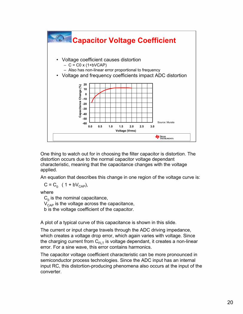
One thing to watch out for in choosing the filter capacitor is distortion. The distortion occurs due to the normal capacitor voltage dependant characteristic, meaning that the capacitance changes with the voltage applied. An equation that describes this change in one region of the voltage curve is:
C = C0 ( 1 + bVCAP), where
C0 is the nominal capacitance, VCAP is the voltage across the capacitance, b is the voltage coefficient of the capacitor.
A plot of a typical curve of this capacitance is shown in this slide.The current or input charge travels through the ADC driving impedance, which creates a voltage drop error, which again varies with voltage. Since the charging current from CFLT is voltage dependant, it creates a non-linear error. For a sine wave, this error contains harmonics. The capacitor voltage coefficient characteristic can be more pronounced in semiconductor process technologies. Since the ADC input has an internal input RC, this distortion-producing phenomena also occurs at the input of the converter.
21
Capacitor THD+N versus Frequency
Silver Mica
-100THD
+ N
(dB
)
-105
-90
-95
-80
-85
-70
-75
-60
-65
-110200 500 1k 20k 50k 10k10k2k 5k 200k100
System Measurement
X7R
Z5U
Y5V
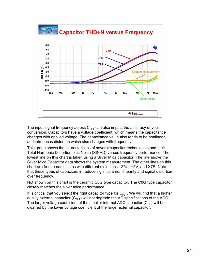
The input signal frequency across CFLT can also impact the accuracy of your conversion. Capacitors have a voltage coefficient, which means the capacitance changes with applied voltage. The capacitance value also tends to be nonlinear, and introduces distortion which also changes with frequency. This graph shows the characteristics of several capacitor technologies and their Total Harmonic Distortion plus Noise (SINAD) versus frequency performance. The lowest line on this chart is taken using a Silver Mica capacitor. The line above the Silver Mica Capacitor data shows the system measurement. The other lines on this chart are from ceramic caps with different dielectrics - Z5U, Y5V, and X7R. Note that these types of capacitors introduce significant non-linearity and signal distortion over frequency.Not shown on this chart is the ceramic C0G type capacitor. The C0G type capacitor closely matches the silver mica performanceIt is critical that you select the right capacitor type for CFLT. We will find that a higher quality external capacitor (CFLT) will not degrade the AC specifications of the ADC. The larger voltage coefficient of the smaller internal ADC capacitor (CSH) will be dwarfed by the lower voltage coefficient of the larger external capacitor.
22
CFLT Type and Value Requirements
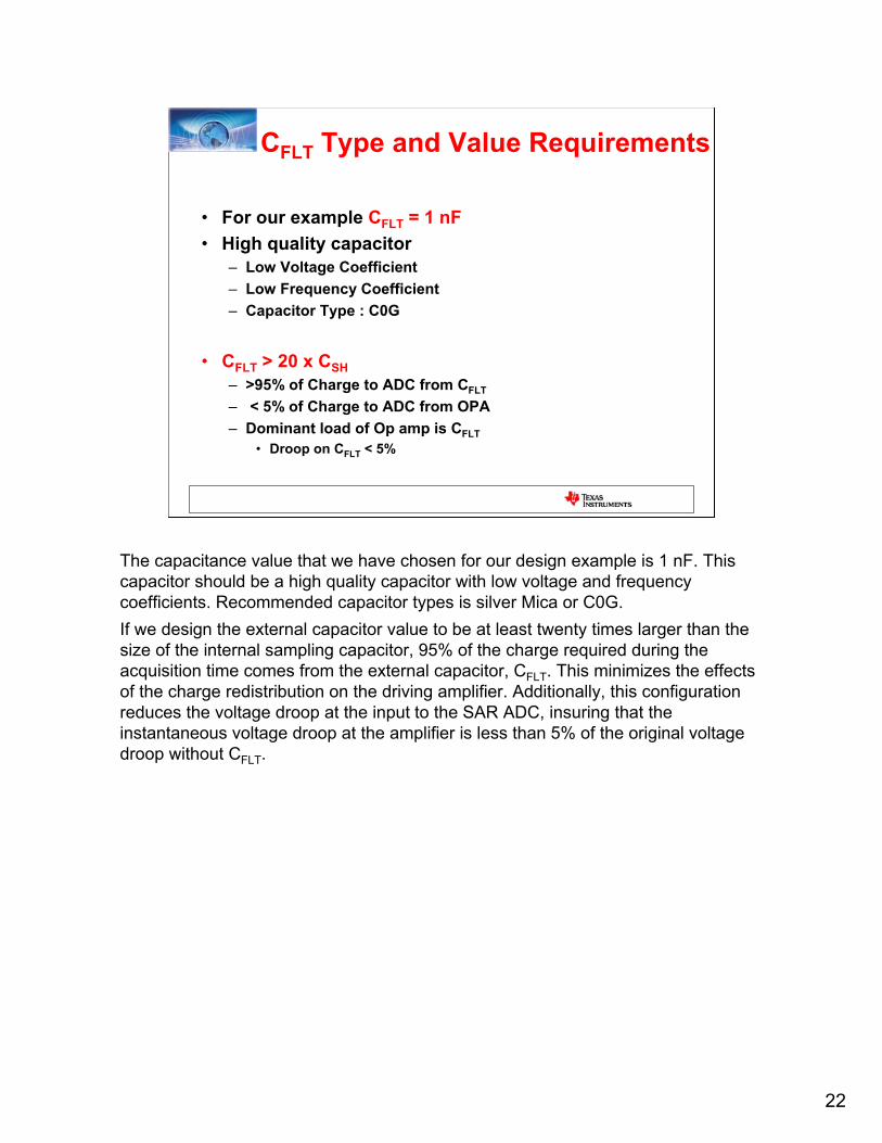
• For our example CFLT = 1 nF• High quality capacitor
– Low Voltage Coefficient– Low Frequency Coefficient– Capacitor Type : C0G
• CFLT > 20 x CSH– >95% of Charge to ADC from CFLT
– < 5% of Charge to ADC from OPA– Dominant load of Op amp is CFLT
• Droop on CFLT < 5%
The capacitance value that we have chosen for our design example is 1 nF. This capacitor should be a high quality capacitor with low voltage and frequency coefficients. Recommended capacitor types is silver Mica or C0G.If we design the external capacitor value to be at least twenty times larger than the size of the internal sampling capacitor, 95% of the charge required during the acquisition time comes from the external capacitor, CFLT. This minimizes the effects of the charge redistribution on the driving amplifier. Additionally, this configuration reduces the voltage droop at the input to the SAR ADC, insuring that the instantaneous voltage droop at the amplifier is less than 5% of the original voltage droop without CFLT.
23
4. Choosing RFLT
• Things we need to know– tACQ = ADC acquisition time (1.88 μs)– k = Single-pole time constant multiplier for 16-bit ADC (12)– CFLT = External input capacitor to ADC (1 nF)
+
-
VS
A/DOp AmpFilter
RFLTCFLT
+VCC +VREF
DOUT
A E CD B
0 V
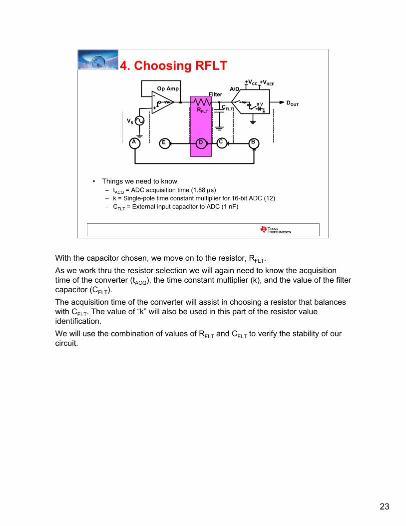
With the capacitor chosen, we move on to the resistor, RFLT.As we work thru the resistor selection we will again need to know the acquisition time of the converter (tACQ), the time constant multiplier (k), and the value of the filtercapacitor (CFLT). The acquisition time of the converter will assist in choosing a resistor that balances with CFLT. The value of “k” will also be used in this part of the resistor value identification. We will use the combination of values of RFLT and CFLT to verify the stability of our circuit.
24
First Pass Determination of RFLT Value
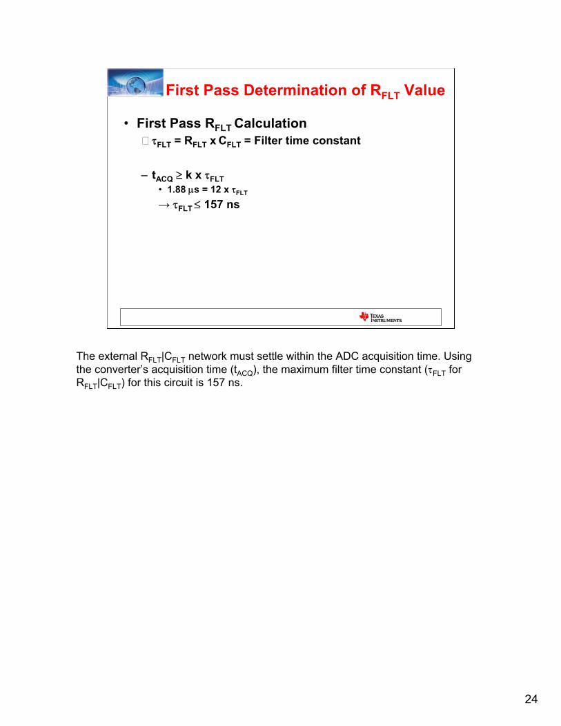
• First Pass RFLT CalculationτFLT = RFLT x CFLT = Filter time constant
– tACQ ≥ k x τFLT• 1.88 μs = 12 x τFLT
→ τFLT ≤ 157 ns
The external RFLT|CFLT network must settle within the ADC acquisition time. Using the converter’s acquisition time (tACQ), the maximum filter time constant (τFLT for RFLT|CFLT) for this circuit is 157 ns.
25
RFLT Value with 40 % Margin
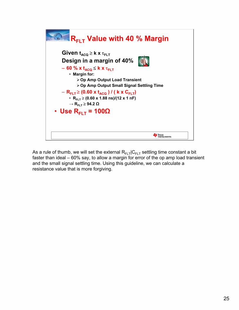
Given tACQ ≥ k x τFLT
Design in a margin of 40%– 60 % x tACQ ≤ k x τFLT
• Margin for:Op Amp Output Load Transient Op Amp Output Small Signal Settling Time
– RFLT ≥ (0.60 x tACQ ) / ( k x CFLT)• RFLT ≥ (0.60 x 1.88 ns)/(12 x 1 nF)→ RFLT ≥ 94.2 Ω
• Use RFLT = 100Ω
As a rule of thumb, we will set the external RFLT|CFLT settling time constant a bit faster than ideal – 60% say, to allow a margin for error of the op amp load transient and the small signal settling time. Using this guideline, we can calculate a resistance value that is more forgiving.
26
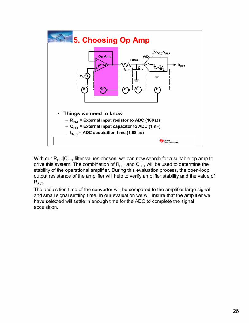
5. Choosing Op Amp
• Things we need to know– RFLT = External input resistor to ADC (100 Ω)– CFLT = External input capacitor to ADC (1 nF)– tACQ = ADC acquisition time (1.88 μs)
+
-
VS
A/DOp AmpFilter
RFLTCFLT
+VCC +VREF
DOUT
A E CD B
0 V
With our RFLT|CFLT filter values chosen, we can now search for a suitable op amp to drive this system. The combination of RFLT and CFLT will be used to determine the stability of the operational amplifier. During this evaluation process, the open-loop output resistance of the amplifier will help to verify amplifier stability and the value of RFLT. The acquisition time of the converter will be compared to the amplifier large signal and small signal settling time. In our evaluation we will insure that the amplifier we have selected will settle in enough time for the ADC to complete the signal acquisition.
27
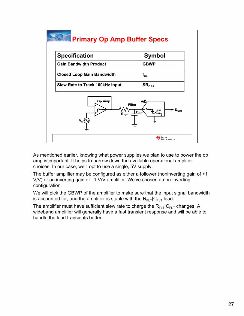
Primary Op Amp Buffer Specs
SROPASlew Rate to Track 100kHz Input
fCLClosed Loop Gain Bandwidth
GBWPGain Bandwidth Product
SymbolSpecification
+
-
VS
A/DOp AmpFilter
RFLTCFLT
DOUT0 V
As mentioned earlier, knowing what power supplies we plan to use to power the op amp is important. It helps to narrow down the available operational amplifier choices. In our case, we’ll opt to use a single, 5V supply.The buffer amplifier may be configured as either a follower (noninverting gain of +1 V/V) or an inverting gain of –1 V/V amplifier. We’ve chosen a non-inverting configuration. We will pick the GBWP of the amplifier to make sure that the input signal bandwidth is accounted for, and the amplifier is stable with the RFLT|CFLT load.The amplifier must have sufficient slew rate to charge the RFLT|CFLT changes. A wideband amplifier will generally have a fast transient response and will be able to handle the load transients better.
28
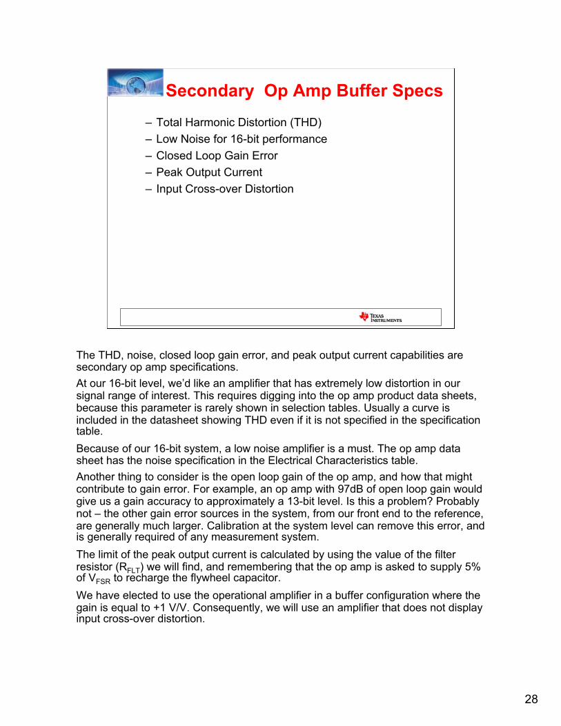
Secondary Op Amp Buffer Specs– Total Harmonic Distortion (THD)– Low Noise for 16-bit performance– Closed Loop Gain Error– Peak Output Current– Input Cross-over Distortion
The THD, noise, closed loop gain error, and peak output current capabilities are secondary op amp specifications. At our 16-bit level, we’d like an amplifier that has extremely low distortion in our signal range of interest. This requires digging into the op amp product data sheets, because this parameter is rarely shown in selection tables. Usually a curve is included in the datasheet showing THD even if it is not specified in the specification table.Because of our 16-bit system, a low noise amplifier is a must. The op amp data sheet has the noise specification in the Electrical Characteristics table. Another thing to consider is the open loop gain of the op amp, and how that might contribute to gain error. For example, an op amp with 97dB of open loop gain would give us a gain accuracy to approximately a 13-bit level. Is this a problem? Probably not – the other gain error sources in the system, from our front end to the reference, are generally much larger. Calibration at the system level can remove this error, and is generally required of any measurement system. The limit of the peak output current is calculated by using the value of the filter resistor (RFLT) we will find, and remembering that the op amp is asked to supply 5% of VFSR to recharge the flywheel capacitor.We have elected to use the operational amplifier in a buffer configuration where the gain is equal to +1 V/V. Consequently, we will use an amplifier that does not display input cross-over distortion.
29
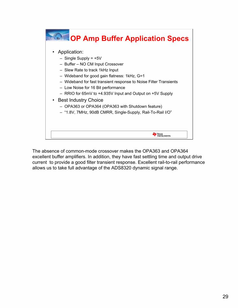
OP Amp Buffer Application Specs• Application:
– Single Supply = +5V– Buffer – NO CM Input Crossover– Slew Rate to track 1kHz Input– Wideband for good gain flatness: 1kHz, G=1– Wideband for fast transient response to Noise Filter Transients– Low Noise for 16 Bit performance– RRIO for 65mV to +4.935V Input and Output on +5V Supply
• Best Industry Choice– OPA363 or OPA364 (OPA363 with Shutdown feature)– “1.8V, 7MHz, 90dB CMRR, Single-Supply, Rail-To-Rail I/O”
The absence of common-mode crossover makes the OPA363 and OPA364 excellent buffer amplifiers. In addition, they have fast settling time and output drive current to provide a good filter transient response. Excellent rail-to-rail performance allows us to take full advantage of the ADS8320 dynamic signal range.
30
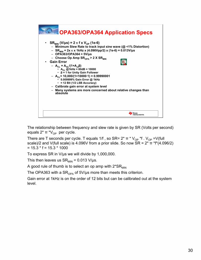
OPA363/OPA364 Application Specs
• SRMIN (V/μs) = 2 π f x VOP (1e-6)– Minimum Slew Rate to track input sine wave (@ <1% Distortion)– SRMIN = 2x π x 1kHz x (4.096Vpp/2) x (1e-6) = 0.013V/μs – OPA363/OPA364 = 5V/μs – Choose Op Amp SROPA > 2 X SRMIN
• Gain Error– ACL = AOL/(1+Aolβ)
• AOL @1kHz = 80dB = 10000 • β = 1 for Unity Gain Follower
– ACL= 10,000/(1+10000·1) = 0.99990001• 0.009999% Gain Error @ 1kHz • ≈ 12 Bit (1/2 LSB Accuracy)
– Calibrate gain error at system level– Many systems are more concerned about relative changes than
absolute
The relationship between frequency and slew rate is given by SR (Volts per second) equals 2* π *VOP per cycle. There are T seconds per cycle. T equals 1/f , so SR= 2* π * VOP *f . VOP =V(full scale)/2 and V(full scale) is 4.096V from a prior slide. So now SR = 2* π *f*(4.096/2) = 15.3 * f = 15.3 * 1000To express SR in V/μs we will divide by 1,000,000.This then leaves us SRMIN = 0.013 V/μs.A good rule of thumb is to select an op amp with 2*SRMIN
The OPA363 with a SROPA of 5V/μs more than meets this criterion.Gain error at 1kHz is on the order of 12 bits but can be calibrated out at the system level.
31
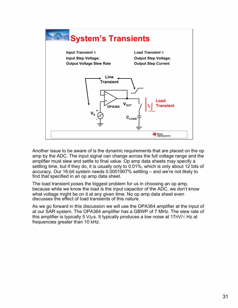
System’s TransientsInput Transient = Load Transient =Input Step Voltage; Output Step Voltage;Output Voltage Slew Rate Output Step Current
+
-
+
-VS
VOUT
CLOAD
LineTransient
LoadTransientITOPA364
Another issue to be aware of is the dynamic requirements that are placed on the op amp by the ADC. The input signal can change across the full voltage range and the amplifier must slew and settle to final value. Op amp data sheets may specify a settling time, but if they do, it is usually only to 0.01%, which is only about 12 bits of accuracy. Our 16-bit system needs 0.0001907% settling – and we’re not likely to find that specified in an op amp data sheet.The load transient poses the biggest problem for us in choosing an op amp, because while we know the load is the input capacitor of the ADC, we don’t know what voltage might be on it at any given time. No op amp data sheet even discusses the effect of load transients of this nature.As we go forward in this discussion we will use the OPA364 amplifier at the input of at our SAR system. The OPA364 amplifier has a GBWP of 7 MHz. The slew rate of this amplifier is typically 5 V/μs. It typically produces a low noise at 17nV/√ Hz at frequencies greater than 10 kHz.
32
Calculating the Op Amp Bandwidth
• Calculate Unity Gain BW– Select Op Amp BW
• GBWP > 4 X fFLT f-3db
• fFLT f-3db = 1/[2πRFLT x CFLT] • fFLT f-3db = 1/[2π x 100Ω x 1 nF] = 1.6 MHz
• Op Amp GBWP >4 x 1.6 MHz = 6.4 MHz
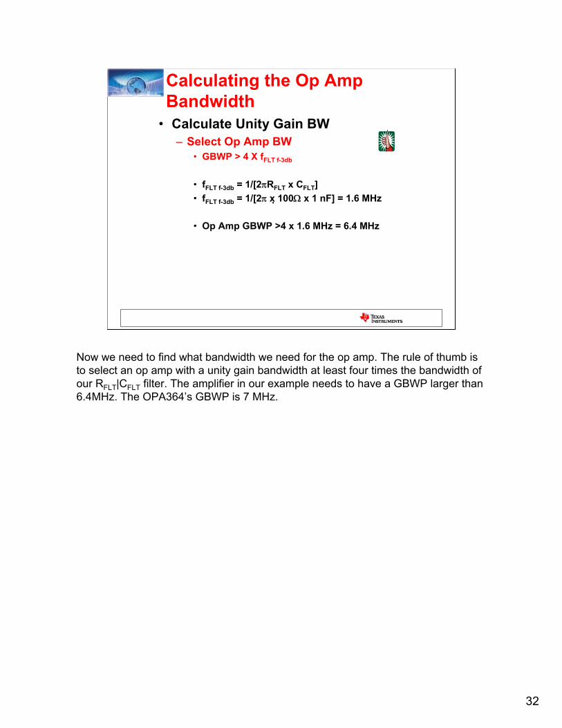
Now we need to find what bandwidth we need for the op amp. The rule of thumb is to select an op amp with a unity gain bandwidth at least four times the bandwidth of our RFLT|CFLT filter. The amplifier in our example needs to have a GBWP larger than 6.4MHz. The OPA364’s GBWP is 7 MHz.
33
• Modify Aol due to RFLT & CFLT– fPX = 1/[2π(RO + RFLT)CFLT]
• fPX = 1/[2π(107Ω + 100Ω)1 nF] = 768kHz– fZX = 1/[2πRFLTCFLT]
• fZX = 1/[2π x100Ω x1 nF] = 1.6MHz
OpAmp + Filter: Small Signal
CFLT
1 nF
100 Ω
RFLT
VOAVFLT
ADS8320
107 Ω
OPA364
+
-
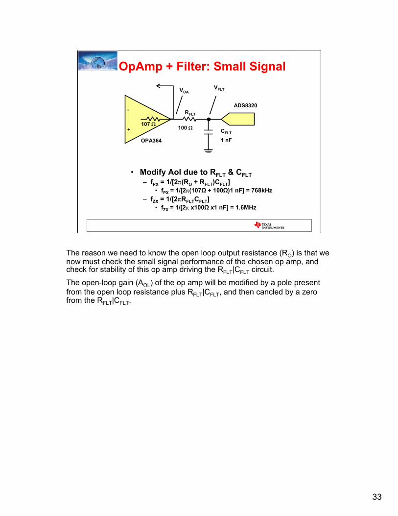
The reason we need to know the open loop output resistance (RO) is that we now must check the small signal performance of the chosen op amp, and check for stability of this op amp driving the RFLT|CFLT circuit.
The open-loop gain (AOL) of the op amp will be modified by a pole present from the open loop resistance plus RFLT|CFLT, and then cancled by a zero from the RFLT|CFLT.
34
OpAmp + Filter: Frequency Response
ACLModified
AOL
fCL3.2 MHz
fPX
fZX
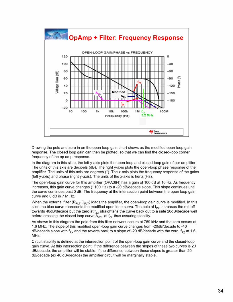
Drawing the pole and zero in on the open-loop gain chart shows us the modified open-loop gain response. The closed loop gain can then be plotted, so that we can find the closed-loop corner frequency of the op amp response.In the diagram in this slide, the left y-axis plots the open-loop and closed-loop gain of our amplifier. The units of this axis are decibels (dB). The right y-axis plots the open-loop phase response of the amplifier. The units of this axis are degrees (°). The x-axis plots the frequency response of the gains (left y-axis) and phase (right y-axis). The units of the x-axis is hertz (Hz). The open-loop gain curve for this amplifier (OPA364) has a gain of 100 dB at 10 Hz. As frequency increases, this gain curve changes (~100 Hz) to a -20 dB/decade slope. This slope continues until the curve continues past 0 dB. The frequency at the intersection point between the open loop gain curve and 0 dB is 7 M Hz. When the external filter (RFLT|CFLT) loads the amplifier, the open-loop gain curve is modified. In this slide the blue curve represents the modified open loop curve. The pole at fPX increases the roll-off towards 40dB/decade but the zero at fZX straightens the curve back out to a safe 20dB/decade well before crossing the closed loop curve AVCL at fCL thus assuring stability.As shown in this diagram the pole from this filter network occurs at 769 kHz and the zero occurs at 1.6 MHz. The slope of this modified open-loop gain curve changes from -20dB/decade to -40 dB/decade slope with fPX and the reverts back to a slope of -20 dB/decade with the zero, fPZ at 1.6 MHz. Circuit stability is defined at the intersection point of the open-loop gain curve and the closed-loop gain curve. At this intersection point, if the difference between the slopes of these two curves is 20 dB/decade, the amplifier will be stable. If the difference between these slopes is greater than 20 dB/decade (ex 40 dB/decade) the amplifier circuit will be marginally stable.
35
OpAmp + Filter: Stability• Buffer Closed Loop Gain Bandwidth as modified by RFLT|CFLT
– fCL = 3.2 MHz
• Stability Check– At fCL = 3.2 MHz “Rate-of-closure” is 20dB/decade fZX cancels fPX
before fCL
• fCL > 2 x fFLT-3dB
– fPX and fZX are < decade apart• Phase of pole will be cancelled by phase of zero
• RO ≤ 9 x RFLT
– fFLT-3db = 1/[2πRFLT x CFLT] = 1.6MHz
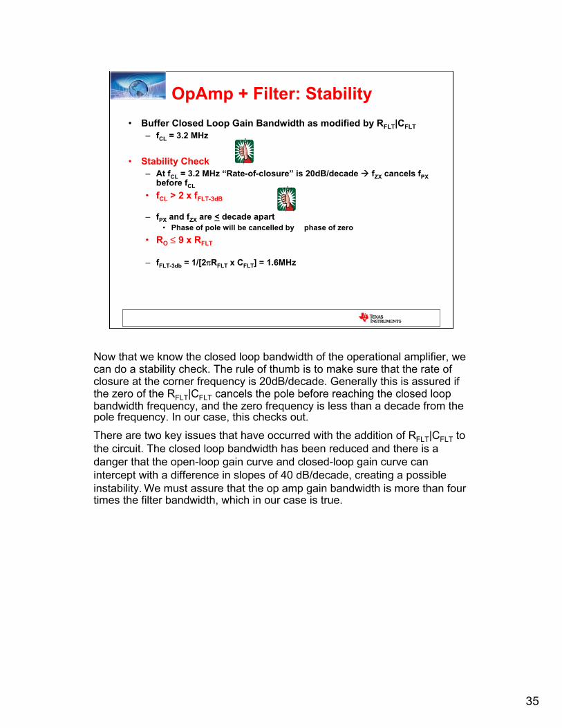
Now that we know the closed loop bandwidth of the operational amplifier, we can do a stability check. The rule of thumb is to make sure that the rate of closure at the corner frequency is 20dB/decade. Generally this is assured if the zero of the RFLT|CFLT cancels the pole before reaching the closed loop bandwidth frequency, and the zero frequency is less than a decade from the pole frequency. In our case, this checks out.
There are two key issues that have occurred with the addition of RFLT|CFLT to the circuit. The closed loop bandwidth has been reduced and there is a danger that the open-loop gain curve and closed-loop gain curve can intercept with a difference in slopes of 40 dB/decade, creating a possible instability. We must assure that the op amp gain bandwidth is more than four times the filter bandwidth, which in our case is true.
36
Amplifier Selection Guidelines
• Stability insured and Bandwidth exceeds input signal– GBWP > 4 x fS(MAX)
– GBWP ≥ 2 / (π CFLT x RFLT) • RO ≤ 9 x RFLT– fCL > 2 x fFLT-3dB
• Slews fast enough for the input signal– SROPA > 4π x fS(MAX) x VOP x (1e-6)
You should apply the guidelines in this slide when you select our amplifier for this SAR system.
37
Final OPA-SAR Circuit Design
+VCC = 5V
CFLT = 1 nF
RFLT = 100Ω
VS
+
-DigitalOut- IN
+ INADS8320
OPA364
+VCCVREF = 4.096V
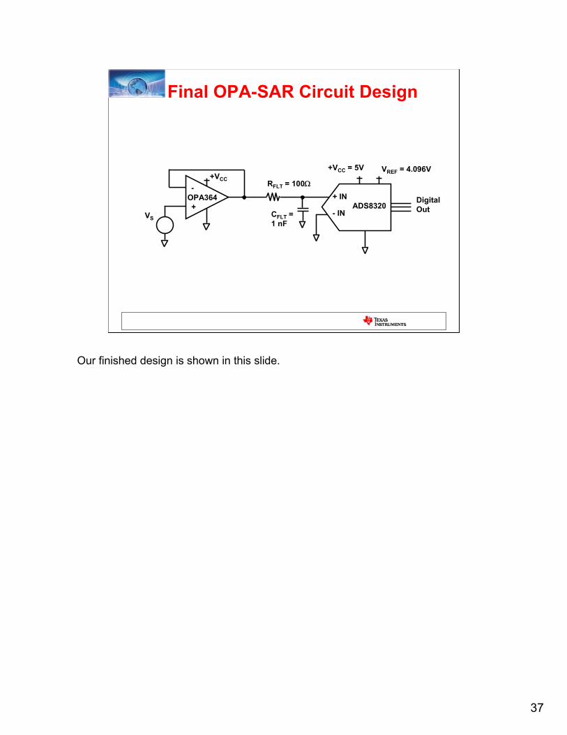
Our finished design is shown in this slide.
38
ADS8320 On Test System
ADS8320
SNR = 88dBENOB = 14.33
InputFrequency
1kHz
InputAmplitude-0.25 dB
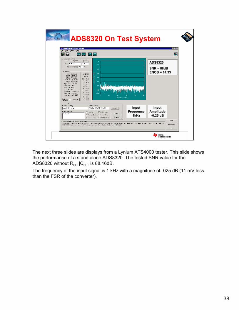
The next three slides are displays from a Lynium ATS4000 tester. This slide shows the performance of a stand alone ADS8320. The tested SNR value for the ADS8320 without RFLT|CFLT is 88.16dB.The frequency of the input signal is 1 kHz with a magnitude of -025 dB (11 mV less than the FSR of the converter).
39
OPA364 + Filter + ADS8320
Op Amp+ Filter+ ADS8320
SNR = 87.78dBENOB = 14.19
InputFrequency
1kHz
InputAmplitude-0.25 dB
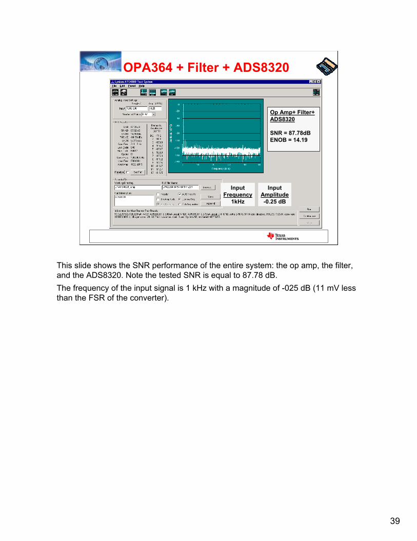
This slide shows the SNR performance of the entire system: the op amp, the filter, and the ADS8320. Note the tested SNR is equal to 87.78 dB.The frequency of the input signal is 1 kHz with a magnitude of -025 dB (11 mV less than the FSR of the converter).
40
Comparison of Tests
ADS8320 Only OPA364, Filter, ADS8320
ADS8320:
SNR = 88dBENOB = 14.33
Op Amp+ Filter+ ADS8320:
SNR = 87.78dBENOB = 14.19
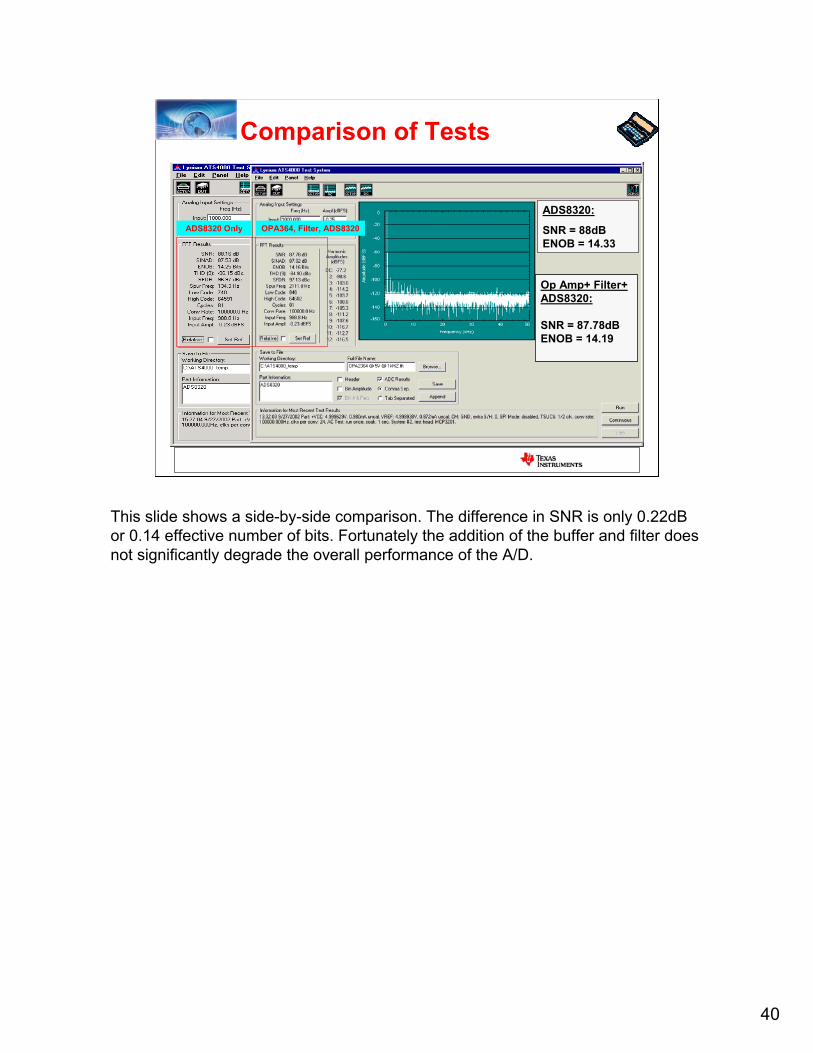
This slide shows a side-by-side comparison. The difference in SNR is only 0.22dB or 0.14 effective number of bits. Fortunately the addition of the buffer and filter does not significantly degrade the overall performance of the A/D.
41
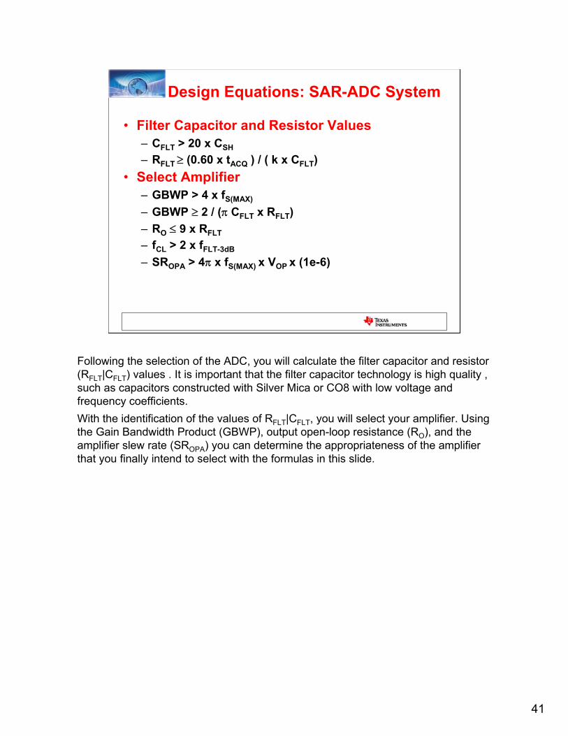
Design Equations: SAR-ADC System
• Filter Capacitor and Resistor Values– CFLT > 20 x CSH– RFLT ≥ (0.60 x tACQ ) / ( k x CFLT)
• Select Amplifier– GBWP > 4 x fS(MAX)
– GBWP ≥ 2 / (π CFLT x RFLT) – RO ≤ 9 x RFLT– fCL > 2 x fFLT-3dB
– SROPA > 4π x fS(MAX) x VOP x (1e-6)
Following the selection of the ADC, you will calculate the filter capacitor and resistor (RFLT|CFLT) values . It is important that the filter capacitor technology is high quality , such as capacitors constructed with Silver Mica or CO8 with low voltage and frequency coefficients. With the identification of the values of RFLT|CFLT, you will select your amplifier. Using the Gain Bandwidth Product (GBWP), output open-loop resistance (RO), and the amplifier slew rate (SROPA) you can determine the appropriateness of the amplifier that you finally intend to select with the formulas in this slide.
42
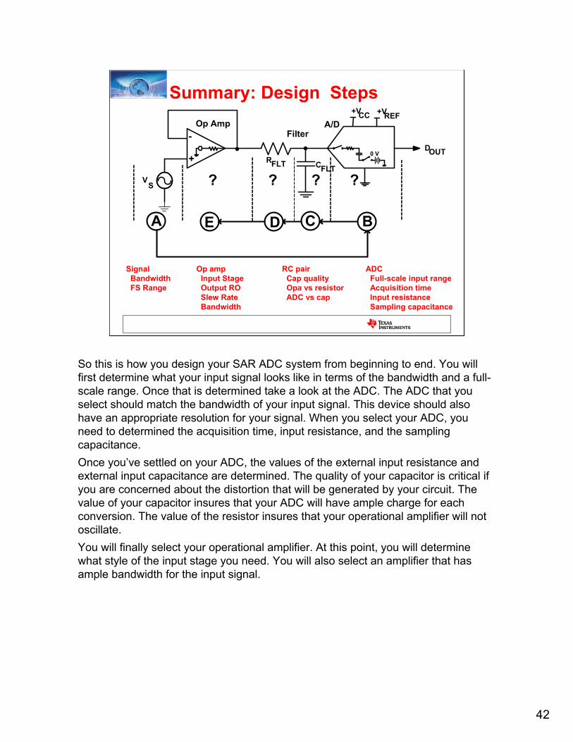
Summary: Design Steps
+
-
VS
A/DOp AmpFilter
RFLT CFLT
+VCC +VREF
DOUT
A
SignalBandwidthFS Range
?
E
Op ampInput StageOutput ROSlew RateBandwidth
?
C
?
D
RC pairCap qualityOpa vs resistorADC vs cap
?
B
ADCFull-scale input rangeAcquisition timeInput resistanceSampling capacitance
0 V
So this is how you design your SAR ADC system from beginning to end. You will first determine what your input signal looks like in terms of the bandwidth and a full-scale range. Once that is determined take a look at the ADC. The ADC that you select should match the bandwidth of your input signal. This device should also have an appropriate resolution for your signal. When you select your ADC, you need to determined the acquisition time, input resistance, and the sampling capacitance. Once you’ve settled on your ADC, the values of the external input resistance and external input capacitance are determined. The quality of your capacitor is critical if you are concerned about the distortion that will be generated by your circuit. The value of your capacitor insures that your ADC will have ample charge for each conversion. The value of the resistor insures that your operational amplifier will not oscillate. You will finally select your operational amplifier. At this point, you will determine what style of the input stage you need. You will also select an amplifier that has ample bandwidth for the input signal.
43
References:Reference 1: Baker, B., Oljaca, M., “Use External components to Improve the Accuracy of a SAR ADC”, EDN 2007Reference 2: Green, Tim, “Operational Amplifier Stability – Part 3 of 15: RO and ROUT”, AnalogZone Acquisition ZoneReference 3: Oljaca, M. and McEldowney, J. (2002.) Using a SAR Analog-to-Digital Converter for Current Measurement in
Motor Control Applications. Burr-Brown Application Report SBAA081.Reference 4: Downs, R. and Oljaca, M. (2005) Designing SAR ADC Drive Circuitry Part II. AnalogZONE: Acquisition Zone.Reference 5: Downs, R., Oljaca, M., “Designing SAR ADC Circuitry – Part 1: A Detailed Look at SAR ADC Operation”,
AnalogZone: Acquisition ZoneReference 6: Downs, R., Oljaca, M., “Designing SAR ADC Drive Circuitry – Part 3: Designing the Optimal Input Drive Circuit
for SAR ADCs”, AnalogZone Acquisition ZoneReference 7: Green, T. (2005) “Operational Amplifier Stability - Part 6 of 15: Capacitance-Load Stability: RISO, High Gain &
CF, Noise Gain” AnalogZONE: Acquisition Zone.Reference 8: Baker, Bonnie, “A Glossary of Analog-to-Digital Specifications and Performance Characteristics”, Texas
Instruments, SBAA147
Symbols:ACL = Operational Amplifier closed loop gainAOL = Operational Amplifier open loop gainb = the voltage coefficient of the capacitorC0 = nominal capacitance of a capacitorCFLT = External filter capacitor between Op Amp and SAR ADCCSH = Input sampling capacitance of SAR ADCfCL = Op Amp Closed Loop Gain BandwidthfFLT-3dB = fPX = Pole that effects open-loop gain response of an amplifier. Generated by RO + RFLT and CFLT
fS = Input Signal frequency for the SAR-ADC systemfS(MAX) = Maximum Input Signal frequency for the SAR-ADC systemFSR = Full-scale signal rangefZX = Zero that effects open-loop gain response of an amplifier. Generated by RFLT and CFLT
GBWP = Gain Bandwidth Productk = Single pole time constant multiplier to calculate converter settling timeQFLT = Charge on the external filter capacitor (CFLT) in SAR ADC systemQSH = Charge on the internal sampling capacitor (CSH) of SAR ADCRFLT = External filter resistor between Op Amp and SAR ADCRO = Open-loop output resistance of an operational amplifierRSW = Parasitic switch resistance at input of SAR ADCS1 = Sampling switch at the input of the SAR ADCS2 = Switch to charge CSH to VSH0 prior to signal acquisitionSRMIN = minimum Slew Rate required to track a 1 kHz signal with < 1% distortionSROPA = Op Amp Slew Rate tACQ = ADC acquisition timetCONV = ADC conversion timeVCAP = the voltage across a capacitorVCC = Positive power supply voltageVFSR = Full-scale voltage input range of ADCVS = Input signal for the SAR ADC systemVOP = Output voltage of Op AmpVREF = Voltage reference for the ADC. For the ADS8320 VREF = VFSR
τADC = Time constant of input structure of ADC equalling RSW x CSH
τFLT = Time constant of RFLT and CFLT
τFLT* = Time constant of RFLT and CFLT with a 40% margin
44
Optimize Your SAR ADC Design


![SAR data.ppt [Μόνο για ανάγνωση] · Introduction – Active microwave Radar ... distance from the transmitter to the ... Microsoft PowerPoint - SAR data.ppt ...](https://static.fdocument.org/doc/165x107/5aea1e197f8b9a36698ca182/sar-datappt-active-microwave-radar-distance.jpg)