PE42553 - pSemiPE42553 UltraCMOS® SPDT RF Switch DOC-62463-2 – (11/2014) Page 3 Recommended...
19
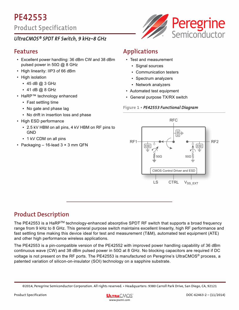
PE42553 Product Specification UltraCMOS® SPDT RF Switch, 9 kHz–8 GHz ©2014, Peregrine Semiconductor Corporation. All rights reserved. • Headquarters: 9380 Carroll Park Drive, San Diego, CA, 92121 Product Specification DOC-62463-2 – (11/2014) www.psemi.com Features • Excellent power handling: 36 dBm CW and 38 dBm pulsed power in 50Ω @ 8 GHz • High linearity: IIP3 of 66 dBm • High isolation ▪ 45 dB @ 3 GHz ▪ 41 dB @ 8 GHz • HaRP™ technology enhanced ▪ Fast settling time ▪ No gate and phase lag ▪ No drift in insertion loss and phase • High ESD performance ▪ 2.5 kV HBM on all pins, 4 kV HBM on RF pins to GND ▪ 1 kV CDM on all pins • Packaging – 16-lead 3 × 3 mm QFN Applications • Test and measurement ▪ Signal sources ▪ Communication testers ▪ Spectrum analyzers ▪ Network analyzers • Automated test equipment • General purpose TX/RX switch Product Description The PE42553 is a HaRP TM technology-enhanced absorptive SPDT RF switch that supports a broad frequency range from 9 kHz to 8 GHz. This general purpose switch maintains excellent linearity, high RF performance and fast settling time making this device ideal for test and measurement (T&M), automated test equipment (ATE) and other high performance wireless applications. The PE42553 is a pin-compatible version of the PE42552 with improved power handling capability of 36 dBm continuous wave (CW) and 38 dBm pulsed power in 50Ω at 8 GHz. No blocking capacitors are required if DC voltage is not present on the RF ports. The PE42553 is manufactured on Peregrine’s UltraCMOS ® process, a patented variation of silicon-on-insulator (SOI) technology on a sapphire substrate. Figure 1 • PE42553 Functional Diagram RFC 50Ω 50Ω CMOS Control Driver and ESD RF2 RF1 LS CTRL V SS_EXT
Transcript of PE42553 - pSemiPE42553 UltraCMOS® SPDT RF Switch DOC-62463-2 – (11/2014) Page 3 Recommended...
PE42553Product SpecificationUltraCMOS® SPDT RF Switch, 9 kHz–8 GHz
Features• Excellent power handling: 36 dBm CW and 38 dBm
pulsed power in 50Ω @ 8 GHz• High linearity: IIP3 of 66 dBm• High isolation
▪ 45 dB @ 3 GHz▪ 41 dB @ 8 GHz
• HaRP™ technology enhanced▪ Fast settling time▪ No gate and phase lag▪ No drift in insertion loss and phase
• High ESD performance▪ 2.5 kV HBM on all pins, 4 kV HBM on RF pins to
GND▪ 1 kV CDM on all pins
• Packaging – 16-lead 3 × 3 mm QFN
Applications• Test and measurement
▪ Signal sources▪ Communication testers▪ Spectrum analyzers▪ Network analyzers
• Automated test equipment• General purpose TX/RX switch
Product DescriptionThe PE42553 is a HaRPTM technology-enhanced absorptive SPDT RF switch that supports a broad frequency range from 9 kHz to 8 GHz. This general purpose switch maintains excellent linearity, high RF performance and fast settling time making this device ideal for test and measurement (T&M), automated test equipment (ATE) and other high performance wireless applications.
The PE42553 is a pin-compatible version of the PE42552 with improved power handling capability of 36 dBm continuous wave (CW) and 38 dBm pulsed power in 50Ω at 8 GHz. No blocking capacitors are required if DC voltage is not present on the RF ports. The PE42553 is manufactured on Peregrine’s UltraCMOS® process, a patented variation of silicon-on-insulator (SOI) technology on a sapphire substrate.
Figure 1 • PE42553 Functional Diagram
RFC
50Ω 50Ω
CMOS Control Driver and ESD
RF2RF1
LS CTRL VSS_EXT
©2014, Peregrine Semiconductor Corporation. All rights reserved. • Headquarters: 9380 Carroll Park Drive, San Diego, CA, 92121
Product Specification DOC-62463-2 – (11/2014)www.psemi.com
PE42553UltraCMOS® SPDT RF Switch
Peregrine’s HaRP technology enhancements deliver high linearity and excellent harmonics performance. It is an innovative feature of the UltraCMOS process, offering the performance of GaAs with the economy and integration of conventional CMOS.
Optional External VSS Control For proper operation, the VSS_EXT control pin must be grounded or tied to the VSS voltage specified in Table 2. When the VSS_EXT control pin is grounded, FETs in the switch are biased with an internal negative voltage generator. For applications that require the lowest possible spur performance, VSS_EXT can be applied externally to bypass the internal negative voltage generator.
Absolute Maximum RatingsExceeding absolute maximum ratings listed in Table 1 may cause permanent damage. Operation should be restricted to the limits in Table 2. Operation between operating range maximum and absolute maximum for extended periods may reduce reliability.
ESD PrecautionsWhen handling this UltraCMOS device, observe the same precautions as with any other ESD-sensitive devices. Although this device contains circuitry to protect it from damage due to ESD, precautions should be taken to avoid exceeding the rating specified in Table 1.
Latch-up ImmunityUnlike conventional CMOS devices, UltraCMOS devices are immune to latch-up.
Table 1 • Absolute Maximum Ratings for PE42553
Parameter/Condition Min Max Unit
Supply voltage, VDD –0.3 5.5 V
Digital input voltage, CTRL –0.3 3.6 V
LS input voltage –0.3 3.6 V
RF input power, CW (RFC–RFX)(1)
9 kHz–10 MHz>10 MHz–8 GHz
Fig. 2, Fig. 337
dBmdBm
RF input power, pulsed (RFC–RFX)(2)
9 kHz–10 MHz>10 MHz–8 GHz
Fig. 2, Fig. 3Fig. 4, Fig. 5
dBmdBm
RF input power into terminated ports, CW (RFX)(1)
9–800 kHz>800 kHz–8 GHz
Fig. 2, Fig. 328
dBmdBm
Storage temperature range –65 +150 °C
ESD voltage HBM(3)
RF pins to GNDAll pins
40002500
VV
Page 2 DOC-62463-2 – (11/2014)www.psemi.com
PE42553UltraCMOS® SPDT RF Switch
Recommended Operating ConditionsTable 2 list the recommending operating condition for PE42553. Devices should not be operated outside the recommended operating conditions listed below.
ESD voltage MM, all pins(4) 200 V
ESD voltage CDM, all pins(5) 1000 V
Notes: 1) 100% duty cycle, all bands, 50Ω.2) Pulsed, 5% duty cycle of 4620 μs period, 50Ω.3) Human body model (MIL-STD 883 Method 3015).4) Machine model (JEDEC JESD22-A115).5) Charged device model (JEDEC JESD22-C101).
Table 2 • Recommended Operating Condition for PE42553
Parameter Min Typ Max Unit
Normal mode (VSS_EXT = 0V)(1)
Supply voltage, VDD 2.3 5.5 V
Supply current, IDD 120 200 μA
Bypass mode (VSS_EXT = –3.4V, VDD ≥ 3.4V for full spec. compliance)(2)
Supply voltage, VDD 2.6 3.4 5.5 V
Supply current, IDD 50 80 μA
Negative supply voltage, VSS_EXT –3.6 –2.6 V
Negative supply current, ISS –40 –16 μA
Normal or Bypass mode
Digital input high, CTRL 1.17 3.6 V
Digital input low, CTRL –0.3 0.6 V
Digital input current, ICTRL 10 μA
RF input power, CW (RFC–RFX)(3)
9 kHz–10 MHz>10 MHz–8 GHz
Fig. 2, Fig. 336
dBmdBm
RF input power, pulsed (RFC–RFX)(4)
9 kHz–10 MHz>10 MHz–8 GHz
Fig. 2, Fig. 3Fig. 4, Fig. 5
dBmdBm
Table 1 • Absolute Maximum Ratings for PE42553
Parameter/Condition Min Max Unit
DOC-62463-2 – (11/2014) Page 3www.psemi.com
PE42553UltraCMOS® SPDT RF Switch
Electrical SpecificationsTable 3 provides the PE42553 key electrical specifications at 25 °C (ZS = ZL = 50Ω), unless otherwise specified. Normal mode(1) is at VDD = 3.3V and VSS_EXT = 0V. Bypass mode(2) is at VDD = 3.4V and VSS_EXT = –3.4V.
RF input power, hot switch, CW(3)
9–300 kHz>300 kHz–8 GHz
Fig. 2, Fig. 320
dBmdBm
RF input power into terminated ports, CW (RFX)(3)
9–600 kHz>600 kHz–8 GHz
Fig. 2, Fig. 326
dBmdBm
Operating temperature range –40 +25 +85 °C
Notes: 1) Normal mode: connect VSS_EXT (pin 13) to GND (VSS_EXT = 0V) to enable internal negative voltage generator.
2) Bypass mode: use VSS_EXT (pin 13) to bypass and disable internal negative voltage generator.
3) 100% duty cycle, all bands, 50Ω.4) Pulsed, 5% duty cycle of 4620 μs period, 50Ω.
Table 3 • PE42553 Electrical Specifications
Parameter Path Condition Min Typ Max Unit
Operating frequency 9 kHz 8 GHz As shown
Insertion loss RFC–RFX9 kHz–10 MHz10 MHz–3 GHz3–8 GHz
0.600.800.85
0.801.001.05
dBdBdB
Isolation
RFX–RFX9 kHz–10 MHz10 MHz–3 GHz3–8 GHz
704633
905436
dBdBdB
RFC–RFX9 kHz–10 MHz10 MHz–3 GHz3–8 GHz
804238
904541
dBdBdB
Return loss (active port) RFC–RFX9 kHz–10 MHz10 MHz–3 GHz3–8 GHz
231715
dBdBdB
Return loss (RFC port) RFC–RFX
9 kHz–10 MHz10 MHz–3 GHz3–8 GHz
231715
dBdBdB
Return loss(terminated port) RFX
9 kHz–10 MHz10 MHz–3 GHz3–8 GHz
322419
dBdBdB
Table 2 • Recommended Operating Condition for PE42553 (Cont.)
Parameter Min Typ Max Unit
Page 4 DOC-62463-2 – (11/2014)www.psemi.com
PE42553UltraCMOS® SPDT RF Switch
Switching FrequencyThe PE42553 has a maximum 25 kHz switching rate in normal mode (pin 13 tied to ground). A faster switching rate is available in bypass mode (pin 13 tied to VSS_EXT). The rate at which the PE42553 can be switched is then limited to the switching time as specified in Table 3.
Switching frequency describes the time duration between switching events. Switching time is the time duration between the point the control signal reached 50% of the final value and the point the output signal reaches within 10% or 90% of its target value.
Spur-Free Performance The typical spurious performance of the PE42553 in normal mode is –152 dBm (pin 13 tied to ground). If spur-free performance is desired, the internal negative voltage generator can be disabled by applying a negative voltage to VSS_EXT (pin 13).
Logic SelectThe Logic Select feature is used to determine the definition for the CTRL pin.
Control LogicTable 4 provides the control logic truth table for the PE42553.
Input 0.1dB compression point(3) RFC–RFX 10 MHz–8 GHz Fig. 4
Fig. 5dBmdBm
Input IP2 RFC–RFX 834 MHz, 1950 MHz 120 dBm
Input IP3 RFC–RFX 834 MHz, 1950 MHz and 2700 MHz 66 dBm
Settling time 50% CTRL to 0.05 dB final value 15 20 μs
Switching time 50% CTRL to 90% or 10% of RF 5.5 9.5 μs
Notes: 1) Normal mode: connect VSS_EXT (pin 29) to GND (VSS_EXT = 0V) to enable internal negative voltage generator.
2) Bypass mode: use VSS_EXT (pin 29) to bypass and disable internal negative voltage generator.
3) The input 0.1dB compression point is a linearity figure of merit. Refer to Table 2 for the RF input power (50Ω).
Table 3 • PE42553 Electrical Specifications
Parameter Path Condition Min Typ Max Unit
Table 4 • Truth Table for PE42553
LS CTRL RFC–RF1 RFC–RF2
0 0 OFF ON
0 1 ON OFF
1 0 ON OFF
1 1 OFF ON
DOC-62463-2 – (11/2014) Page 5www.psemi.com
PE42553UltraCMOS® SPDT RF Switch
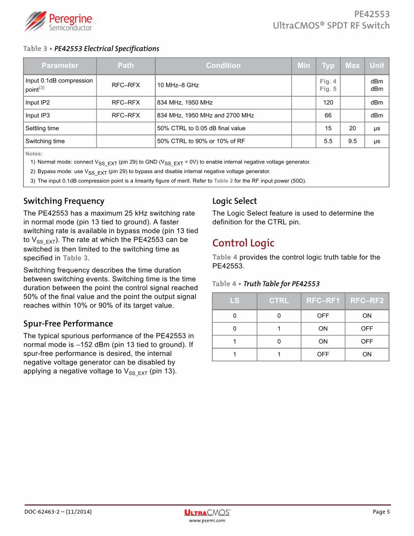
Figure 2 • Power De-rating Curve for 9 kHz–10 MHz @ 25 °C Ambient (50Ω)(*)
Note: * VSS_EXT = –VDD.
Figure 3 • Power De-rating Curve for 9 kHz–10 MHz @ 85 °C Ambient (50Ω)(*)
Note: * VSS_EXT = –VDD.
0
5
10
15
20
25
30
35
40
1 10 100 1000 10000
Inpu
t Pow
er (d
Bm
)
Frequency (kHz)
2.6 Vdd 2.8 Vdd 3.0 Vdd 3.2 Vdd 3.4 Vdd
0
5
10
15
20
25
30
35
40
1 10 100 1000 10000
Inpu
t Pow
er (d
Bm
)
Frequency (kHz)
2.6 VDD 2.8 VDD 3.0 VDD 3.2 VDD 3.4 VDD
Page 6 DOC-62463-2 – (11/2014)www.psemi.com
PE42553UltraCMOS® SPDT RF Switch
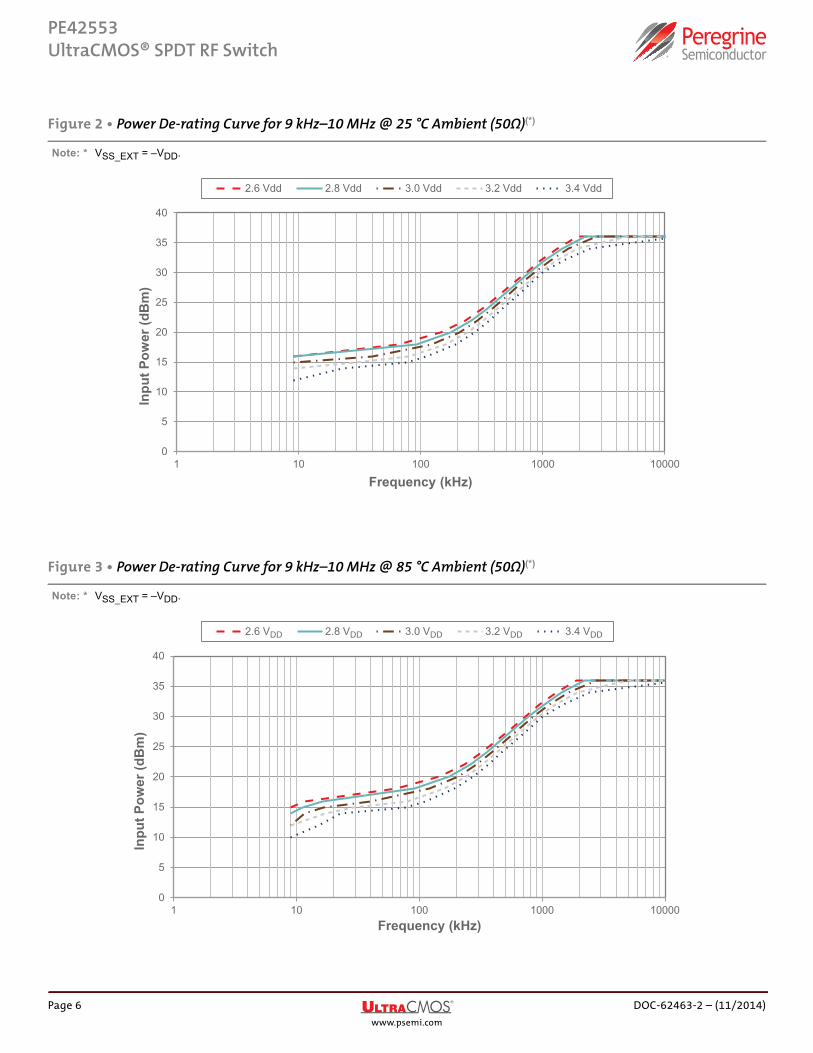
Figure 4 • Power De-rating Curve for 10 MHz–8 GHz @ 25 °C Ambient (50Ω)(*)
Note: * Normal mode at 2.3V ≥ VDD ≥ 5.5V and VSS_EXT = 0V, Bypass mode at VDD = 3.4V and VSS_EXT = –3.4V.
Figure 5 • Power De-rating Curve for 10 MHz–8 GHz @ 85 °C Ambient (50Ω)(*)
Note: * Normal mode at 2.3V ≥ VDD ≥ 5.5V and VSS_EXT = 0V, Bypass mode at VDD = 3.4V and VSS_EXT = –3.4V.
34.535
35.536
36.537
37.538
38.539
39.540
40.541
41.5
0 1 2 3 4 5 6 7 8
Inpu
t Pow
er (d
Bm
)
Frequency (GHz)
P0.1dB Compression / Abs. Max. RF Input Power, Pulsed @ 25°C Ambient
Max. RF Input Power, Pulsed @ 25°C Ambient
Max. RF Input Power, CW @ 25°C Ambient
34.5
35
35.5
36
36.5
37
37.5
38
38.5
39
39.5
40
40.5
41
0 1 2 3 4 5 6 7 8
Inpu
t Pow
er (d
Bm
)
Frequency (GHz)
P0.1dB Compression / Abs. Max. RF Input Power, Pulsed @ 85°C Ambient
Max. RF Input Power, Pulsed @ 85°C Ambient
Max. RF Input Power, CW @ 85°C Ambient
DOC-62463-2 – (11/2014) Page 7www.psemi.com
PE42553UltraCMOS® SPDT RF Switch
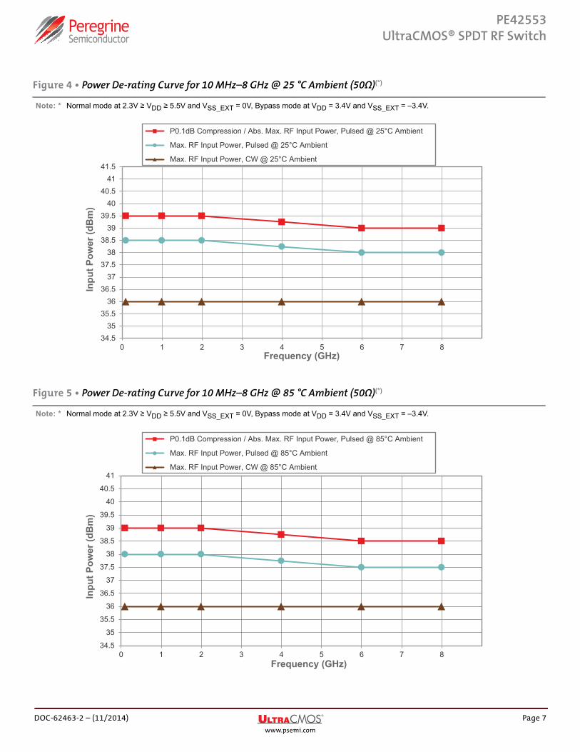
Typical Performance DataFigure 6–Figure 17 show the typical performance data @ 25 °C and VDD = 3.4V (ZS = ZL = 50Ω), unless otherwise specified.
Figure 6 • Insertion Loss vs Temperature (RFC–RFX)
0 1 2 3 4 5 6 7 8
Inse
rtio
n Lo
ss (d
B)
Frequency (GHz)
− 40°C +25°C +85°C
−5
−4.5
−4
−3.5
−3
−2.5
−2
−1.5
−1
−0.5
0
Page 8 DOC-62463-2 – (11/2014)www.psemi.com
PE42553UltraCMOS® SPDT RF Switch
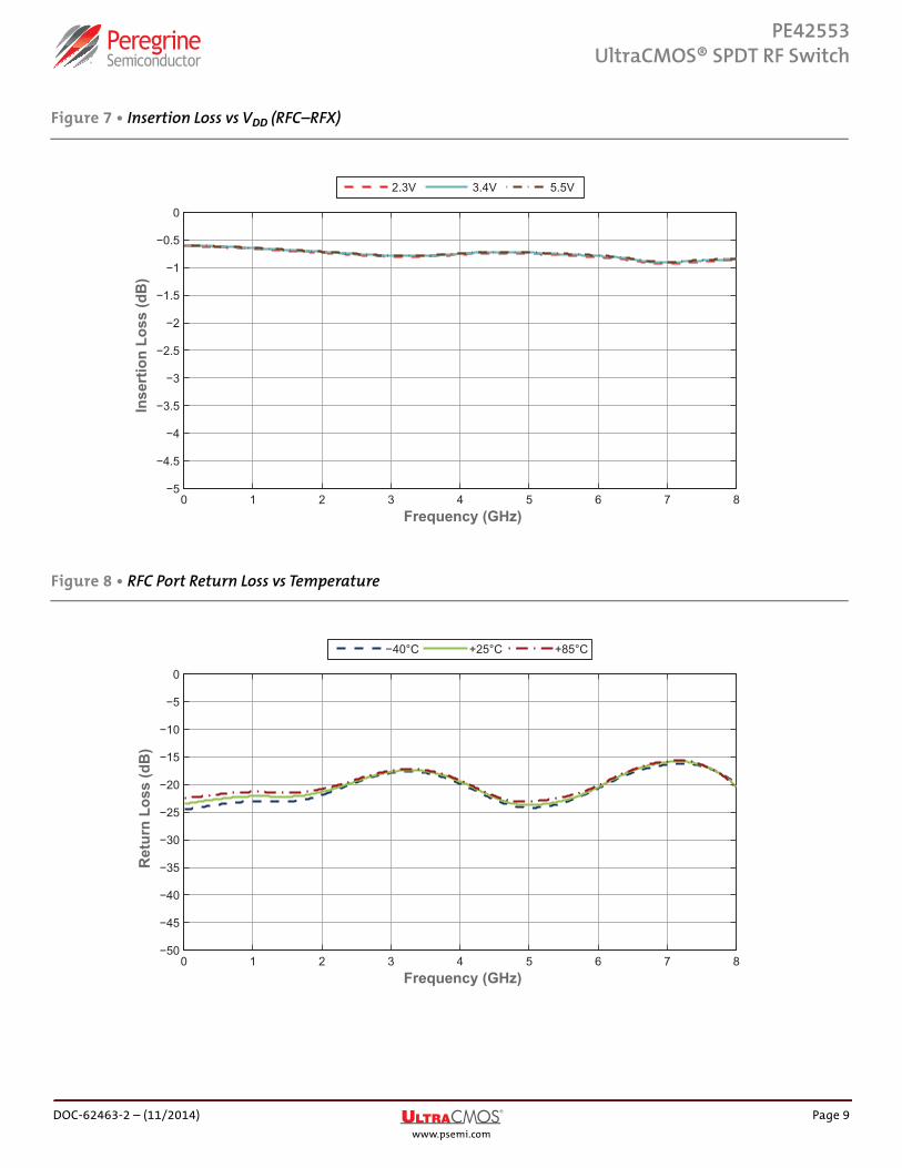
Figure 7 • Insertion Loss vs VDD (RFC–RFX)
Figure 8 • RFC Port Return Loss vs Temperature
0 1 2 3 4 5 6 7 8−5
−4.5
−4
−3.5
−3
−2.5
−2
−1.5
−1
−0.5
0
Inse
rtio
n Lo
ss (d
B)
Frequency (GHz)
2.3V 3.4V 5.5V
0 1 2 3 4 5 6 7 8−50
−45
−40
−35
−30
−25
−20
−15
−10
−5
0
Ret
urn
Loss
(dB
)
Frequency (GHz)
− 40°C +25°C +85°C
DOC-62463-2 – (11/2014) Page 9www.psemi.com
PE42553UltraCMOS® SPDT RF Switch
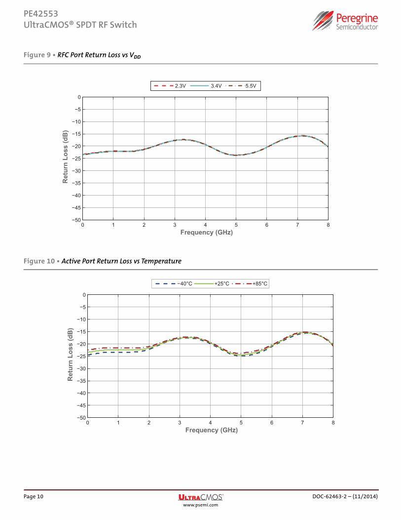
Figure 9 • RFC Port Return Loss vs VDD
Figure 10 • Active Port Return Loss vs Temperature
0 1 2 3 4 5 6 7 8−50
−45
−40
−35
−30
−25
−20
−15
−10
−5
0
Ret
urn
Loss
(dB
)
Frequency (GHz)
2.3V 3.4V 5.5V
0 1 2 3 4 5 6 7 8−50
−45
−40
−35
−30
−25
−20
−15
−10
−5
0
Ret
urn
Loss
(dB
)
Frequency (GHz)
− 40°C +25°C +85°C
Page 10 DOC-62463-2 – (11/2014)www.psemi.com
PE42553UltraCMOS® SPDT RF Switch
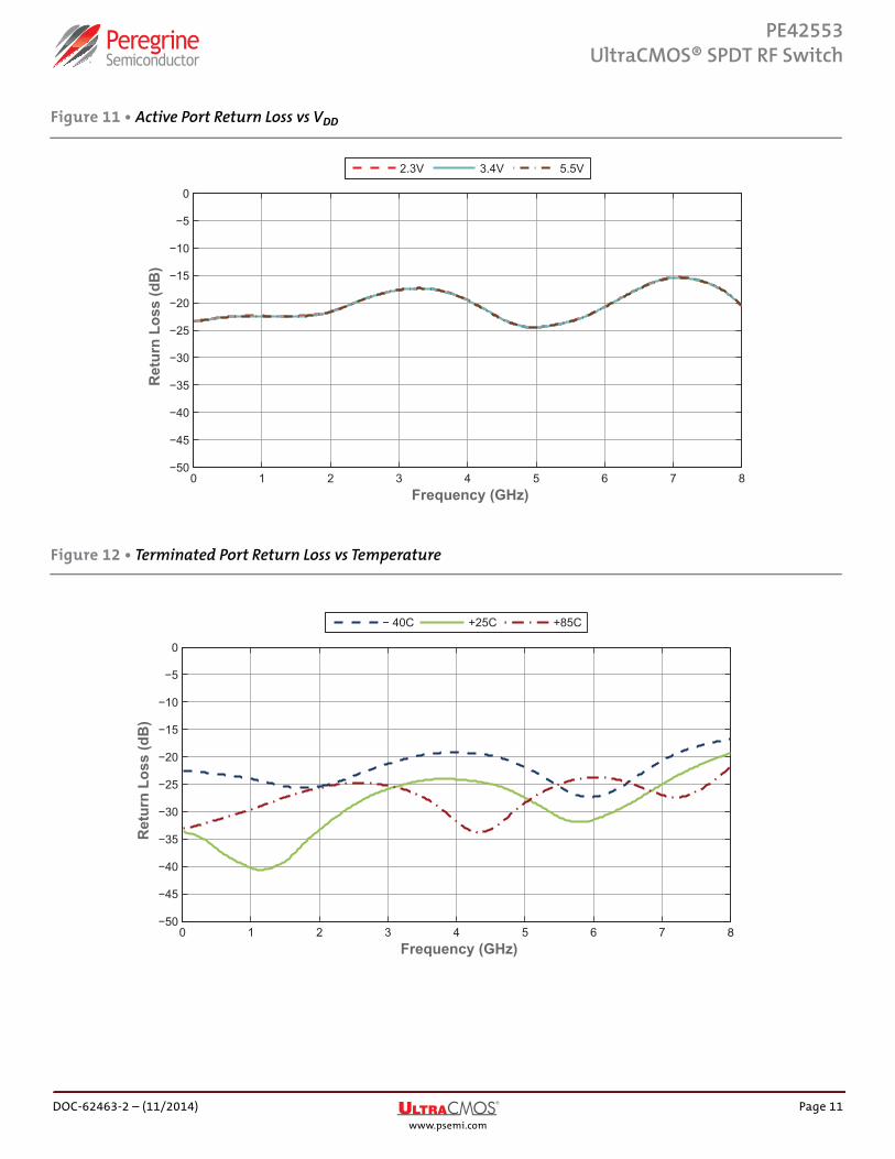
Figure 11 • Active Port Return Loss vs VDD
Figure 12 • Terminated Port Return Loss vs Temperature
0 1 2 3 4 5 6 7 8−50
−45
−40
−35
−30
−25
−20
−15
−10
−5
0
Ret
urn
Loss
(dB
)
Frequency (GHz)
2.3V 3.4V 5.5V
0 1 2 3 4 5 6 7 8−50
−45
−40
−35
−30
−25
−20
−15
−10
−5
0
Ret
urn
Loss
(dB
)
Frequency (GHz)
− 40C +25C +85C
DOC-62463-2 – (11/2014) Page 11www.psemi.com
PE42553UltraCMOS® SPDT RF Switch
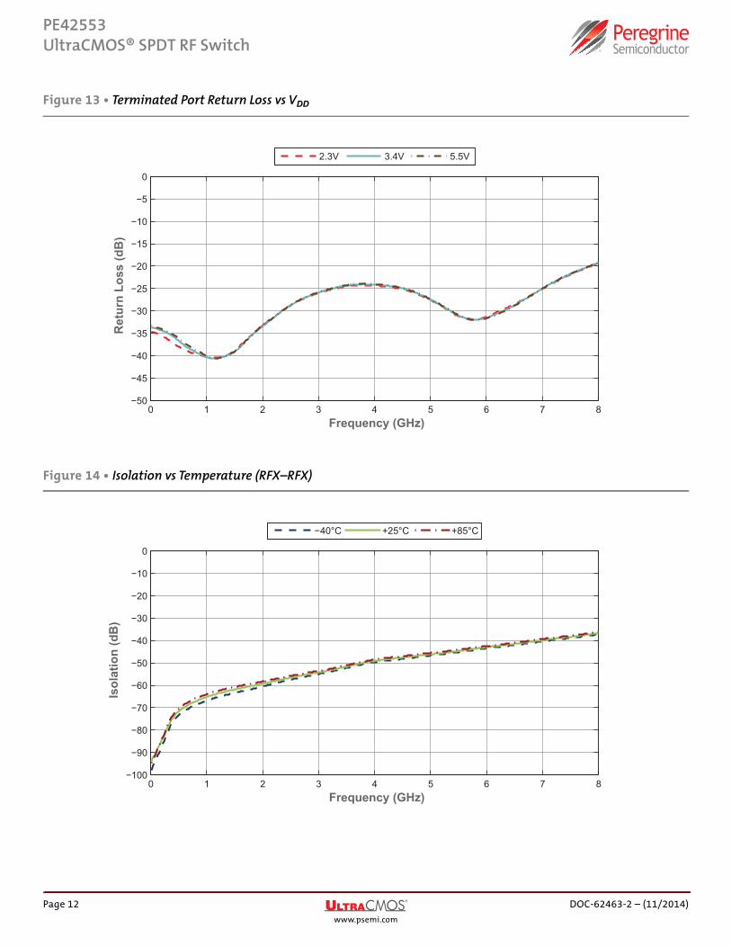
Figure 13 • Terminated Port Return Loss vs VDD
Figure 14 • Isolation vs Temperature (RFX–RFX)
0 1 2 3 4 5 6 7 8−50
−45
−40
−35
−30
−25
−20
−15
−10
−5
0
Ret
urn
Loss
(dB
)
Frequency (GHz)
2.3V 3.4V 5.5V
0 1 2 3 4 5 6 7 8−100
−90
−80
−70
−60
−50
−40
−30
−20
−10
0
Frequency (GHz)
Isol
atio
n (d
B)
− 40°C +25°C +85°C
Page 12 DOC-62463-2 – (11/2014)www.psemi.com
PE42553UltraCMOS® SPDT RF Switch
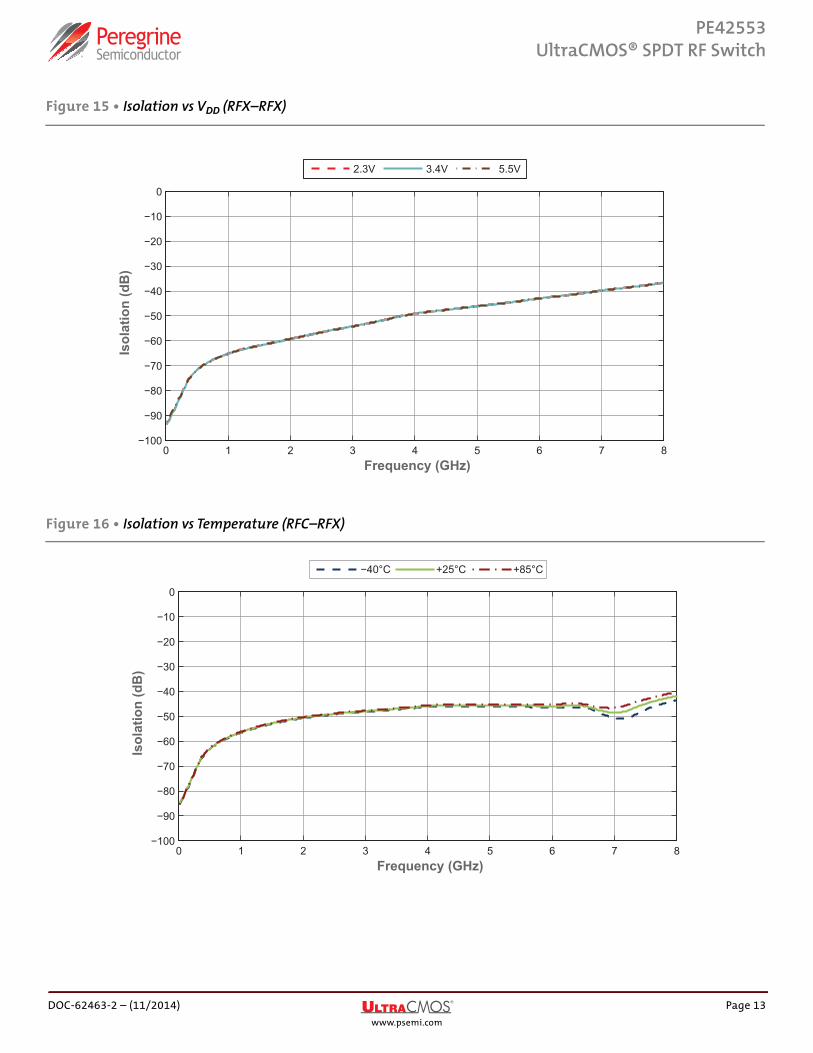
Figure 15 • Isolation vs VDD (RFX–RFX)
Figure 16 • Isolation vs Temperature (RFC–RFX)
0 1 2 3 4 5 6 7 8−100
−90
−80
−70
−60
−50
−40
−30
−20
−10
0
Frequency (GHz)
Isol
atio
n (d
B)
2.3V 3.4V 5.5V
0 1 2 3 4 5 6 7 8−100
−90
−80
−70
−60
−50
−40
−30
−20
−10
0
Frequency (GHz)
Isol
atio
n (d
B)
−40°C +25°C +85°C
DOC-62463-2 – (11/2014) Page 13www.psemi.com
PE42553UltraCMOS® SPDT RF Switch
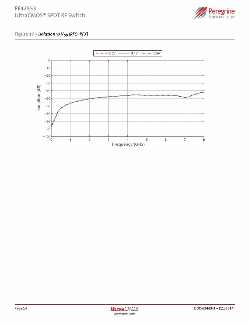
Figure 17 • Isolation vs VDD (RFC–RFX)
0 1 2 3 4 5 6 7 8−100
−90
−80
−70
−60
−50
−40
−30
−20
−10
0
Frequency (GHz)
Isol
atio
n (d
B)
2.3V 3.4V 5.5V
Page 14 DOC-62463-2 – (11/2014)www.psemi.com
PE42553UltraCMOS® SPDT RF Switch
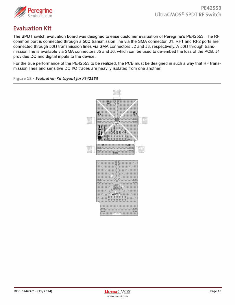
Evaluation Kit The SPDT switch evaluation board was designed to ease customer evaluation of Peregrine’s PE42553. The RF common port is connected through a 50Ω transmission line via the SMA connector, J1. RF1 and RF2 ports are connected through 50Ω transmission lines via SMA connectors J2 and J3, respectively. A 50Ω through trans-mission line is available via SMA connectors J5 and J6, which can be used to de-embed the loss of the PCB. J4 provides DC and digital inputs to the device.
For the true performance of the PE42553 to be realized, the PCB must be designed in such a way that RF trans-mission lines and sensitive DC I/O traces are heavily isolated from one another.
Figure 18 • Evaluation Kit Layout for PE42553
DOC-62463-2 – (11/2014) Page 15www.psemi.com
PE42553UltraCMOS® SPDT RF Switch
Pin InformationThis section provides pinout information for the PE42553. Figure 19 shows the pin map of this device for the available package. Table 5 provides a description for each pin.
Figure 19 • Pin Configuration (Top View)
ExposedGround Pad
GND
RF1
GND
GND
GN
D
GN
D
RFC
GN
D
GND
RF2
GND
GND
VD
D
LS CTR
L
VS
S_E
XT
1
3
2
4
12
10
11
9
5 76 8
16 1415 13Pin 1 DotMarking
Table 5 • Pin Descriptions for PE42553
Pin No. Pin Name Description
1, 3–6, 8–10, 12 GND Ground.
2 RF1(1) RF port 1.
7 RFC(1) RF common.
11 RF2(1) RF port 2.
13 VSS_EXT(2) External VSS negative voltage control.
14 CTRL Digital control logic input.
15 LSLogic Select – used to determine the definition for the CTRL pin (see Table 4).
16 VDD Supply voltage.
Pad GND Exposed pad: ground for proper oper-ation.
Notes: 1) RF pins 2, 7 and 11 must be at 0 VDC. The RF pins do not require
DC blocking capacitors for proper operation if the 0 VDC requirement is met.
2) Use VSS_EXT (pin 13) to bypass and disable internal negative voltage generator. Connect VSS_EXT (pin 13) to GND (VSS_EXT = 0V) to enable internal negative voltage generator.
Page 16 DOC-62463-2 – (11/2014)www.psemi.com
PE42553UltraCMOS® SPDT RF Switch
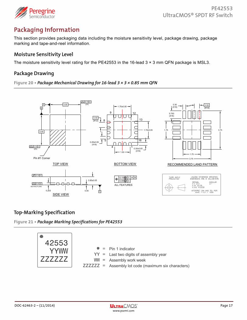
Packaging InformationThis section provides packaging data including the moisture sensitivity level, package drawing, package marking and tape-and-reel information.
Moisture Sensitivity LevelThe moisture sensitivity level rating for the PE42553 in the 16-lead 3 × 3 mm QFN package is MSL3.
Package Drawing
Top-Marking Specification
Figure 20 • Package Mechanical Drawing for 16-lead 3 × 3 × 0.85 mm QFN
Figure 21 • Package Marking Specifications for PE42553
TOP VIEW
SIDE VIEW
BOTTOM VIEW
3.00
3.00
Pin #1 Corner
1.70±0.05
0.85±0.05
0.050.203
RECOMMENDED LAND PATTERN
13
16
14
5
9
8
12
1.70±0.05
0.50
0.25±0.05(X16)
1.50
0.30±0.05(X16)
1.75
3.75
3.75
0.10 C A B0.05 C
A
0.10 C(2X)
C
0.10 C
0.05 C
SEATING PLANE
B
ALL FEATURES
0.10 C(2X)
0.750(X16)
0.30(X16)
0.50
1.75
(X12)
(X12)
=YY =WW =
ZZZZZZ =
Pin 1 indicatorLast two digits of assembly yearAssembly work weekAssembly lot code (maximum six characters)
42553YYWW
ZZZZZZ
DOC-62463-2 – (11/2014) Page 17www.psemi.com
PE42553UltraCMOS® SPDT RF Switch
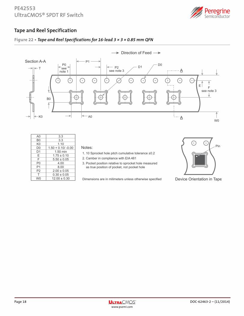
Tape and Reel Specification
Figure 22 • Tape and Reel Specifications for 16-lead 3 × 3 × 0.85 mm QFN
T
K0 A0
B0
P0P1
D1A
Section A-A
A
Direction of Feed
D0
E
W0
P2see note 3
seenote 1
Fsee note 3
A0B0K0D0D1EF
P0P1P2T
W0
3.33.3
1.101.50 + 0.10/ -0.00
1.50 min1.75 ± 0.105.50 ± 0.05
4.008.00
2.00 ± 0.050.30 ± 0.05
12.00 ± 0.30 Device Orientation in Tape
Pin 1Notes:1. 10 Sprocket hole pitch cumulative tolerance ±0.22. Camber in compliance with EIA 4813. Pocket position relative to sprocket hole measured
as true position of pocket, not pocket hole
Dimensions are in milimeters unless otherwise specified
Page 18 DOC-62463-2 – (11/2014)www.psemi.com
PE42553 UltraCMOS® SPDT RF Switch
Ordering InformationTable 6 lists the available ordering codes for the PE42553 as well as available shipping methods.
Table 6 • Order Codes for PE42553
Order Codes Description Packaging Shipping Method
PE42553A-Z PE42553 SPDT RF switch Green 16-lead 3 × 3 mm QFN 3000 units / T&R
EK42553-01 PE42553 Evaluation kit Evaluation kit 1 / Box
Product Specification www.psemi.com DOC-62463-2 – (11/2014)
Document CategoriesAdvance InformationThe product is in a formative or design stage. The datasheet containsdesign target specifications for product development. Specificationsand features may change in any manner without notice.
Preliminary SpecificationThe datasheet contains preliminary data. Additional data may be addedat a later date. Peregrine reserves the right to change specifications atany time without notice in order to supply the best possible product.
Product SpecificationThe datasheet contains final data. In the event Peregrine decides tochange the specifications, Peregrine will notify customers of theintended changes by issuing a CNF (Customer Notification Form).
Not Recommended for New Designs (NRND)This product is in production but is not recommended for new designs.
End of Life (EOL)This product is currently going through the EOL process. It has aspecific last-time buy date.
ObsoleteThis product is discontinued. Orders are no longer accepted for thisproduct.
Sales Contact For additional information, contact Sales at [email protected].
DisclaimersThe information in this datasheet is believed to be reliable. However, Peregrine assumes no liability for the use of this information. Use shall beentirely at the user’s own risk. No patent rights or licenses to any circuits described in this datasheet are implied or granted to any third party.Peregrine’s products are not designed or intended for use in devices or systems intended for surgical implant, or in other applications intended tosupport or sustain life, or in any application in which the failure of the Peregrine product could create a situation in which personal injury or deathmight occur. Peregrine assumes no liability for damages, including consequential or incidental damages, arising out of the use of its products insuch applications.
Patent StatementPeregrine products are protected under one or more of the following U.S. patents: patents.psemi.com
Copyright and Trademark©2014, Peregrine Semiconductor Corporation. All rights reserved. The Peregrine name, logo, UTSi and UltraCMOS are registered trademarks andHaRP, MultiSwitch and DuNE are trademarks of Peregrine Semiconductor Corp.