
P-channel 40 V, 0.0175 typ.,36 A, STripFET F6 Power MOSFET ...
16
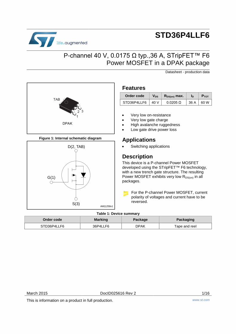
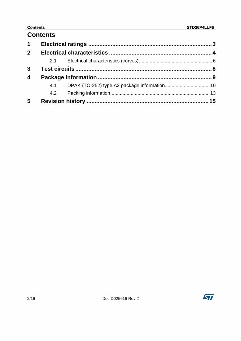
March 2015 DocID025616 Rev 2 1/16 This is information on a product in full production. www.st.com STD36P4LLF6 P-channel 40 V, 0.0175 Ω typ.,36 A, STripFET™ F6 Power MOSFET in a DPAK package Datasheet - production data Figure 1: Internal schematic diagram Features Order code VDS RDS(on) max. ID PTOT STD36P4LLF6 40 V 0.0205 Ω 36 A 60 W • Very low on-resistance • Very low gate charge • High avalanche ruggedness • Low gate drive power loss Applications • Switching applications Description This device is a P-channel Power MOSFET developed using the STripFET™ F6 technology, with a new trench gate structure. The resulting Power MOSFET exhibits very low R DS(on) in all packages. For the P-channel Power MOSFET, current polarity of voltages and current have to be reversed. Table 1: Device summary Order code Marking Package Packaging STD36P4LLF6 36P4LLF6 DPAK Tape and reel AM11258v1 D(2, TAB) S(3) G(1)
Transcript of P-channel 40 V, 0.0175 typ.,36 A, STripFET F6 Power MOSFET ...
March 2015 DocID025616 Rev 2 1/16
This is information on a product in full production. www.st.com
STD36P4LLF6
P-channel 40 V, 0.0175 Ω typ.,36 A, STripFET™ F6 Power MOSFET in a DPAK package
Datasheet - production data
Figure 1: Internal schematic diagram
Features Order code VDS RDS(on) max. ID PTOT
STD36P4LLF6 40 V 0.0205 Ω 36 A 60 W
• Very low on-resistance • Very low gate charge • High avalanche ruggedness • Low gate drive power loss
Applications • Switching applications
Description This device is a P-channel Power MOSFET developed using the STripFET™ F6 technology, with a new trench gate structure. The resulting Power MOSFET exhibits very low RDS(on) in all packages.
For the P-channel Power MOSFET, current polarity of voltages and current have to be reversed.
Table 1: Device summary Order code Marking Package Packaging
STD36P4LLF6 36P4LLF6 DPAK Tape and reel
AM11258v1
D(2, TAB)
S(3)
G(1)
Contents STD36P4LLF6
2/16 DocID025616 Rev 2
Contents 1 Electrical ratings ............................................................................. 3
2 Electrical characteristics ................................................................ 4
2.1 Electrical characteristics (curves) ...................................................... 6
3 Test circuits ..................................................................................... 8
4 Package information ....................................................................... 9
4.1 DPAK (TO-252) type A2 package information................................. 10
4.2 Packing information ......................................................................... 13
5 Revision history ............................................................................ 15
STD36P4LLF6 Electrical ratings
DocID025616 Rev 2 3/16
1 Electrical ratings Table 2: Absolute maximum ratings
Symbol Parameter Value Unit
VDS Drain-source voltage 40 V
VGS Gate-source voltage ± 20 V
ID Drain current (continuous) at TC = 25 °C 36 A
ID Drain current (continuous) at TC = 100 °C 26 A
IDM(1) Drain current (pulsed) 144 A
PTOT Total dissipation at Tc = 25 °C 60 W
Tstg Storage temperature -55 to 175 °C
Tj Maximum junction temperature 175 °C
Notes: (1) Pulse width limited by safe operating area.
Table 3: Thermal data Symbol Parameter Value Unit
Rthj-case Thermal resistance junction-case max 2.5 °C/W
For the P-channel Power MOSFET, current polarity of voltages and current have to be reversed.
Electrical characteristics STD36P4LLF6
4/16 DocID025616 Rev 2
2 Electrical characteristics (TC = 25 °C unless otherwise specified)
Table 4: Static Symbol Parameter Test conditions Min. Typ. Max. Unit
V(BR)DSS Drain-source breakdown voltage VGS = 0 V, ID = 250 µA 40
V
IDSS Zero gate voltage Drain current
VGS = 0 V, VDS = 40 V
1 µA
VGS = 0 V, VDS = 40 V, TC = 125 °C
10 µA
IGSS Gate-body leakage current VDS = 0 V, VGS = ± 20 V
±100 nA
VGS(th) Gate threshold voltage VDS = VGS, ID = 250 µA 1
2.5 V
RDS(on) Static drain-source on-resistance
VGS = 10 V, ID = 18 A
0.0175 0.0205 Ω
VGS = 4.5 V, ID= 18 A
0.024 0.029
Table 5: Dynamic Symbol Parameter Test conditions Min. Typ. Max. Unit
Ciss Input capacitance
VDS = 25 V, f = 1 MHz, VGS = 0 V
- 2850 - pF
Coss Output capacitance - 270 - pF
Crss Reverse transfer capacitance - 180 - pF
Qg Total gate charge VDD = 20 V, ID = 36 A, VGS = 4.5 V (see Figure 14: "Gate charge test circuit")
- 22 - nC
Qgs Gate-source charge - 9.4 - nC
Qgd Gate-drain charge - 7.3 - nC
RG Gate input resistance
ID = 0 A, gate DC bias = 0 V, f = 1 MHz, magnitude of alternative signal = 20 mV
- 1.4 - Ω
Table 6: Switching times
Symbol Parameter Test conditions Min. Typ. Max. Unit
td(on) Turn-on delay time VDD = 20 V, ID = 18 A RG = 4.7 Ω, VGS = 10 V (see Figure 13: "Switching times test circuit for resistive load")
- 43 - ns
tr Rise time - 47 - ns
td(off) Turn-off-delay time - 148 - ns
tf Fall time - 19 - ns
For the P-channel Power MOSFET, current polarity of voltages and current have to be reversed.
STD36P4LLF6 Electrical characteristics
DocID025616 Rev 2 5/16
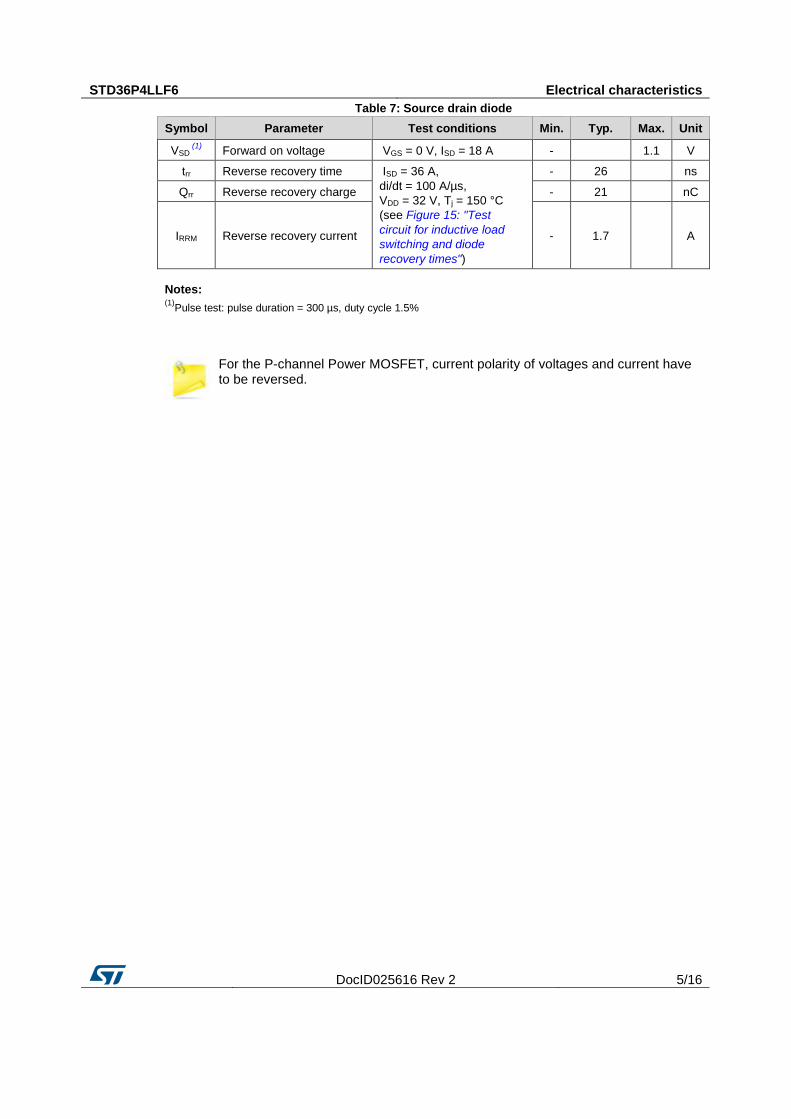
Table 7: Source drain diode Symbol Parameter Test conditions Min. Typ. Max. Unit
VSD (1) Forward on voltage VGS = 0 V, ISD = 18 A -
1.1 V
trr Reverse recovery time ISD = 36 A, di/dt = 100 A/µs, VDD = 32 V, Tj = 150 °C (see Figure 15: "Test circuit for inductive load switching and diode recovery times")
- 26
ns
Qrr Reverse recovery charge - 21
nC
IRRM Reverse recovery current - 1.7
A
Notes: (1)Pulse test: pulse duration = 300 µs, duty cycle 1.5%
For the P-channel Power MOSFET, current polarity of voltages and current have to be reversed.
Electrical characteristics STD36P4LLF6
6/16 DocID025616 Rev 2
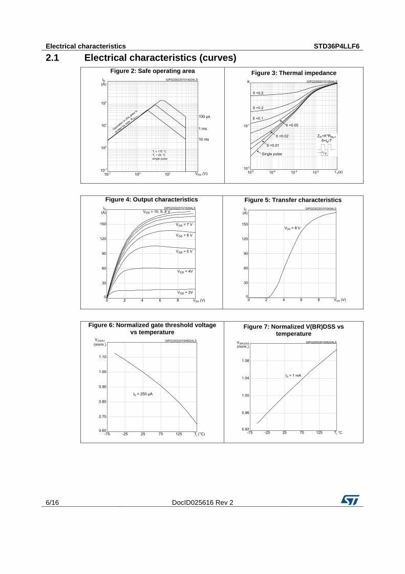
2.1 Electrical characteristics (curves) Figure 2: Safe operating area
Figure 3: Thermal impedance
Figure 4: Output characteristics
Figure 5: Transfer characteristics
Figure 6: Normalized gate threshold voltage vs temperature
Figure 7: Normalized V(BR)DSS vs temperature
STD36P4LLF6 Electrical characteristics
DocID025616 Rev 2 7/16
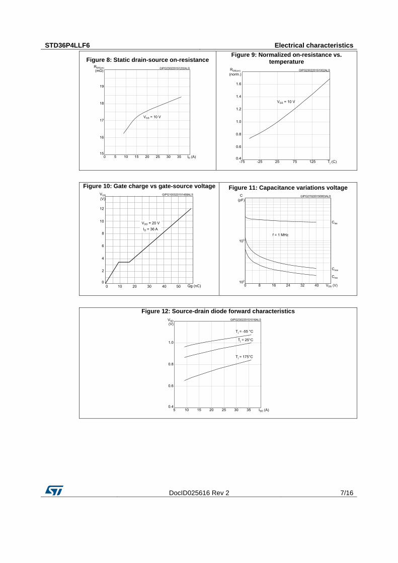
Figure 8: Static drain-source on-resistance
Figure 9: Normalized on-resistance vs. temperature
Figure 10: Gate charge vs gate-source voltage
Figure 11: Capacitance variations voltage
Figure 12: Source-drain diode forward characteristics
Test circuits STD36P4LLF6
8/16 DocID025616 Rev 2
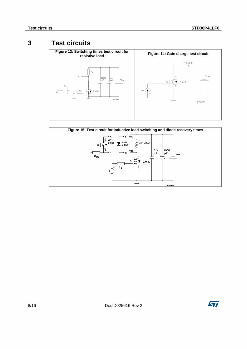
3 Test circuits Figure 13: Switching times test circuit for
resistive load
Figure 14: Gate charge test circuit
Figure 15: Test circuit for inductive load switching and diode recovery times

STD36P4LLF6 Package information
DocID025616 Rev 2 9/16
4 Package information In order to meet environmental requirements, ST offers these devices in different grades of ECOPACK® packages, depending on their level of environmental compliance. ECOPACK® specifications, grade definitions and product status are available at: www.st.com. ECOPACK® is an ST trademark.
Package information STD36P4LLF6
10/16 DocID025616 Rev 2
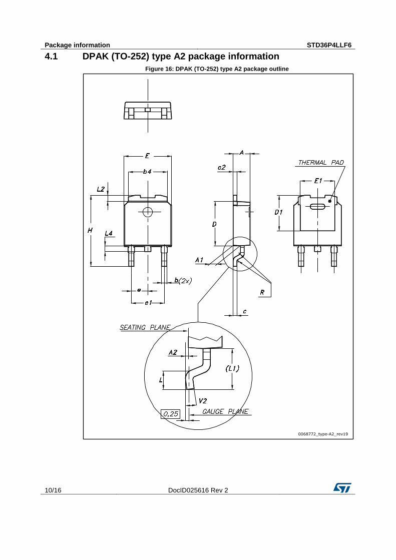
4.1 DPAK (TO-252) type A2 package information Figure 16: DPAK (TO-252) type A2 package outline
STD36P4LLF6 Package information
DocID025616 Rev 2 11/16
Table 8: DPAK (TO-252) type A2 mechanical data
Dim. mm
Min. Typ. Max.
A 2.20
2.40
A1 0.90
1.10
A2 0.03
0.23
b 0.64
0.90
b4 5.20
5.40
c 0.45
0.60
c2 0.48
0.60
D 6.00
6.20
D1 4.95 5.10 5.25
E 6.40
6.60
E1 5.10 5.20 5.30
e 2.16 2.28 2.40
e1 4.40
4.60
H 9.35
10.10
L 1.00
1.50
L1 2.60 2.80 3.00
L2 0.65 0.80 0.95
L4 0.60
1.00
R
0.20
V2 0°
8°
Package information STD36P4LLF6
12/16 DocID025616 Rev 2
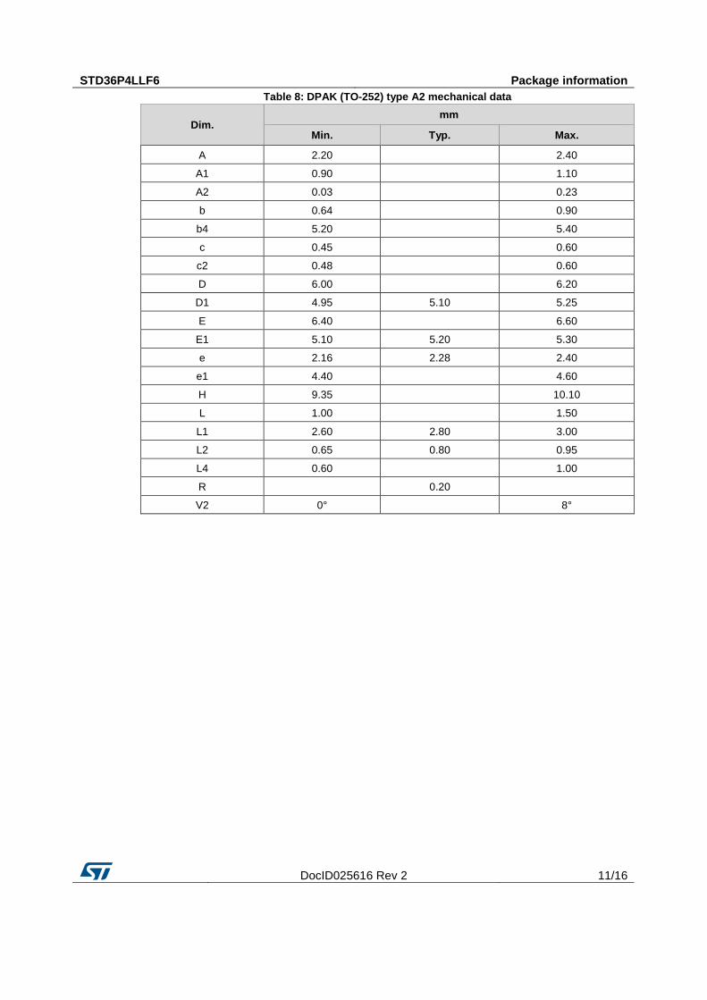
Figure 17: DPAK (TO-252) recommended footprint (dimensions are in mm)
STD36P4LLF6 Package information
DocID025616 Rev 2 13/16
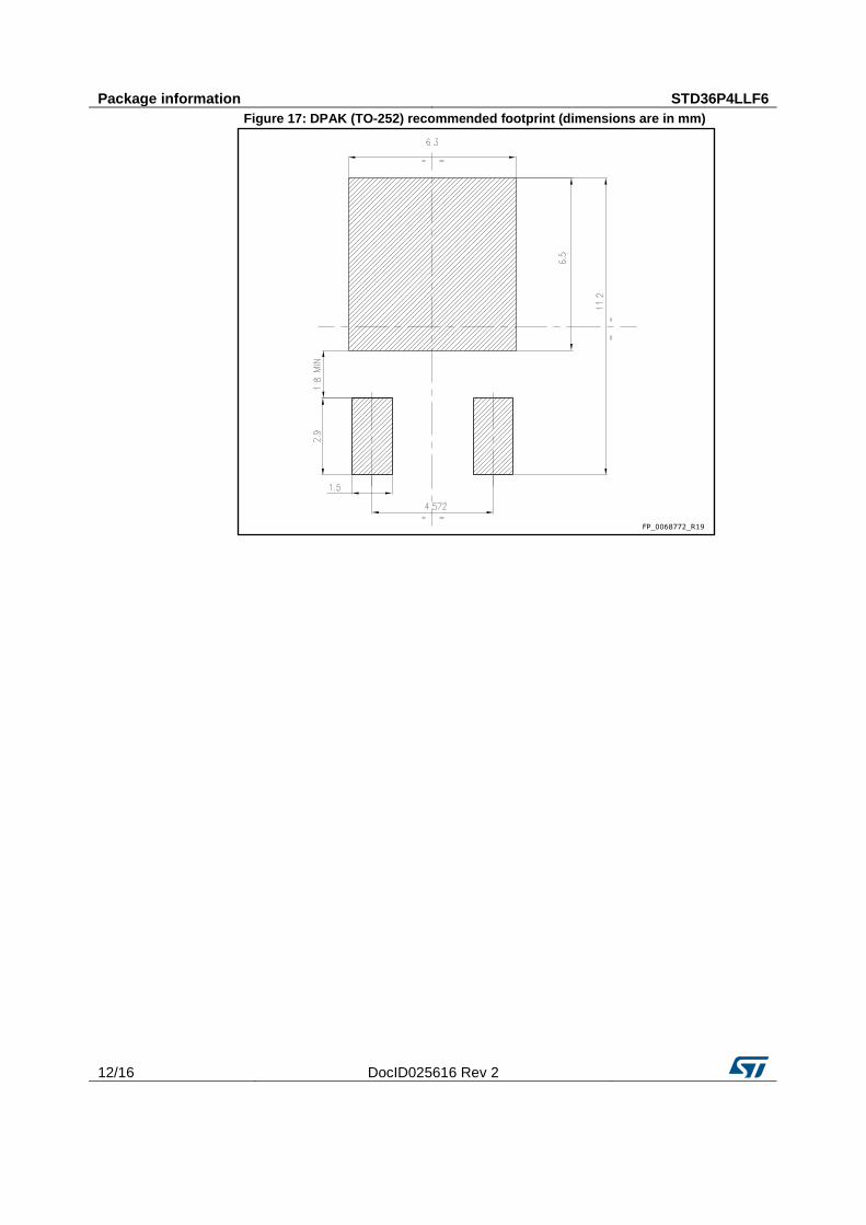
4.2 Packing information Figure 18: Tape for DPAK (TO-252)
P1A0 D1
P0
FW
E
D
B0K0
T
User direction of feed
P2
10 pitches cumulativetolerance on tape +/- 0.2 mm
User direction of feed
R
Bending radius
B1
For machine ref. onlyincluding draft andradii concentric around B0
AM08852v1
Top covertape
Package information STD36P4LLF6
14/16 DocID025616 Rev 2
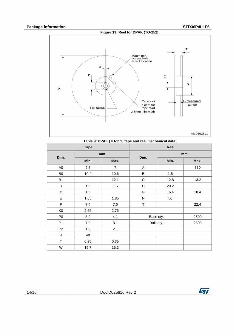
Figure 19: Reel for DPAK (TO-252)
Table 9: DPAK (TO-252) tape and reel mechanical data Tape Reel
Dim. mm
Dim. mm
Min. Max. Min. Max.
A0 6.8 7 A
330
B0 10.4 10.6 B 1.5
B1
12.1 C 12.8 13.2
D 1.5 1.6 D 20.2
D1 1.5
G 16.4 18.4
E 1.65 1.85 N 50
F 7.4 7.6 T
22.4
K0 2.55 2.75
P0 3.9 4.1 Base qty. 2500
P1 7.9 8.1 Bulk qty. 2500
P2 1.9 2.1
R 40
T 0.25 0.35
W 15.7 16.3
A
D
B
Full radius
Tape slotin core fortape start
2.5mm min.width
G measuredat hub
C
N
40mm min.access holeat slot location
T
AM06038v1
STD36P4LLF6 Revision history
DocID025616 Rev 2 15/16
5 Revision history Table 10: Document revision history
Date Revision Changes
10-Dec-2013 1 First revision.
24-Mar-2015 2
Text edits throughout document On cover page, updated title, applications, description and features table Updated Table 4: Static Updated Table 5: Dynamic Updated Table 6: Switching times Updated Table 7: Source-drain diode Added Section 2.1: Electrical characteristics (curves) Minor text changes

STD36P4LLF6
16/16 DocID025616 Rev 2
IMPORTANT NOTICE – PLEASE READ CAREFULLY
STMicroelectronics NV and its subsidiaries (“ST”) reserve the right to make changes, corrections, enhancements, modifications, and improvements to ST products and/or to this document at any time without notice. Purchasers should obtain the latest relevant information on ST products before placing orders. ST products are sold pursuant to ST’s terms and conditions of sale in place at the time of order acknowledgement.
Purchasers are solely responsible for the choice, selection, and use of ST products and ST assumes no liability for application assistance or the design of Purchasers’ products.
No license, express or implied, to any intellectual property right is granted by ST herein.
Resale of ST products with provisions different from the information set forth herein shall void any warranty granted by ST for such product.
ST and the ST logo are trademarks of ST. All other product or service names are the property of their respective owners.
Information in this document supersedes and replaces information previously supplied in any prior versions of this document.
© 2015 STMicroelectronics – All rights reserved