
Optimization of Transistors for Very High Frequency dc-dc ... · 2 + − V IN +-V OUT L F L 2F C 2F...
13
1 Optimization of Transistors for Very High Frequency dc-dc Converters Anthony D. Sagneri † , David I. Anderson ‡ , David J. Perreault † † LABORATORY FOR ELECTROMAGNETIC AND ELECTRONIC SYSTEMS MASSACHUSETTS I NSTITUTE OF TECHNOLOGY,ROOM 10–171 CAMBRIDGE,MASSACHUSETTS 02139 EMAIL: [email protected] ‡ NATIONAL SEMICONDUCTOR CORPORATION 2900 SEMICONDUCTOR DRIVE SANTA CLARA, CA 95052-8090 Abstract—This document presents a method to optimize inte- grated LDMOS transistors for use in very high frequency (VHF, 30-300 MHz) dc-dc converters. A transistor model valid at VHF switching frequencies is developed. Device parameters are related to layout geometry and the resulting layout vs. loss tradeoffs are illustrated. A method of finding an optimal layout for a given converter application is developed and experimentally verified in a 50 MHz converter, resulting in a 35% reduction in power loss over an un-optimized device. It is further demonstrated that hot-carrier limits on device safe operating area may be relaxed under soft switching, yielding significant further loss reduction. A device fabricated with 20-V design rules is validated at 35-V, offering reduced parasitic resistance and capacitance. Compared to the original design, loss is up to 75% lower in the example application. Index Terms—resonant dc-dc converter, resonant boost con- verter, very high frequency, VHF integrated power converter, class Φ inverter, class F power amplifier, class E inverter, resonant gate drive, self-oscillating gate drive, resonant rectifier, harmonic peaking. I. I NTRODUCTION R EDUCTION of size, weight, cost, and greater integration is a continual theme in power conversion. A promising solution uses a resonant power stage with soft-switching and soft-gating operating in the very high frequency (VHF, 30 MHz to 300 MHz) regime. Such converters can achieve very good efficiencies over wide load and input ranges for power levels from a few watts to hundreds of watts [1]–[3]. How- ever, the device losses that dominate in VHF converters are significantly different than under hard-switched operation. As a result only a small subset of commercially available power MOSFETs are suitable for VHF converters. These tend to be discrete RF LDMOSFETs that are expensive and packaged in a manner not suitable for small, integrated converters. On the other hand, while offering a high degree of integration, most semiconductor processes for power conversion are intended for operation at a few megahertz. In this case, optimization for hard-switched operation has driven tradeoffs at the process, design-rule, and layout stages [4]–[6] that produce devices with mediocre VHF performance. This paper shows that good VHF performance is achievable using an integrated power process. In the case of the power process used for this work, much of the improvement derives from the optimization of the device layout. Thus we focus on understanding how device losses in resonant VHF converters differ from those observed under hard switching (Section II). A set of easily measured device parasitics is chosen and used to parametrize a model that predicts device loss given a particular resonant converter circuit. In turn, these parameters are connected to the device layout which permits a layout optimization with device loss as a cost function (Section III). In an example application, a 38% reduction in device loss is achieved as compared to the devices initially available in the power process. Further benefit arises through relaxation of the safe oper- ating area (SOA) constraints normally specified for devices under hard-switched operation (Section IV). In particular, we demonstrate that at least in some power processes devices can be operated under soft-switching at higher peak voltages than their specifications for hard-switching. This means that at a given peak operating voltage devices with smaller parasitic resistance and capacitance can be used, reducing device loss and improving overall converter efficiency. For an example application we show that the combination of layout optimization and relaxation of the SOA leads to better than 57% reduction in device loss for LDMOSFETs fabricated in the available integrated power process. Performance of an optimized device at VHF is verified through the construction and testing of two converters. Results are presented in Sec- tion V. II. VHF DEVICE LOSS MODEL Semiconductor device losses place critical limits on the design and performance of power converters. In hard-switched operation the various loss mechanisms are usually split into conduction loss, switching loss (often subdivided into overlap loss and capacitive discharge loss), and gating loss [3]. Unlike conduction loss, the switching and gating losses are frequency dependent. Beyond a few megahertz these mechanisms can 1590 978-1-4244-2893-9/09/$25.00 ©2009 IEEE
-
Upload
nguyencong -
Category
Documents
-
view
216 -
download
0
Transcript of Optimization of Transistors for Very High Frequency dc-dc ... · 2 + − V IN +-V OUT L F L 2F C 2F...
1
Optimization of Transistors for Very HighFrequency dc-dc Converters
Anthony D. Sagneri†, David I. Anderson ‡, David J. Perreault†
†LABORATORY FOR ELECTROMAGNETIC AND ELECTRONIC SYSTEMS
MASSACHUSETTS INSTITUTE OF TECHNOLOGY, ROOM 10–171CAMBRIDGE, MASSACHUSETTS 02139
EMAIL: [email protected]
‡NATIONAL SEMICONDUCTOR CORPORATION
2900 SEMICONDUCTOR DRIVE
SANTA CLARA, CA 95052-8090
Abstract—This document presents a method to optimize inte-grated LDMOS transistors for use in very high frequency (VHF,30-300 MHz) dc-dc converters. A transistor model valid at VHFswitching frequencies is developed. Device parameters are relatedto layout geometry and the resulting layout vs. loss tradeoffs areillustrated. A method of finding an optimal layout for a givenconverter application is developed and experimentally verifiedin a 50 MHz converter, resulting in a 35% reduction in powerloss over an un-optimized device. It is further demonstrated thathot-carrier limits on device safe operating area may be relaxedunder soft switching, yielding significant further loss reduction.A device fabricated with 20-V design rules is validated at 35-V,offering reduced parasitic resistance and capacitance. Comparedto the original design, loss is up to 75% lower in the exampleapplication.
Index Terms—resonant dc-dc converter, resonant boost con-verter, very high frequency, VHF integrated power converter,class Φ inverter, class F power amplifier, class E inverter, resonantgate drive, self-oscillating gate drive, resonant rectifier, harmonicpeaking.
I. INTRODUCTION
REDUCTION of size, weight, cost, and greater integrationis a continual theme in power conversion. A promising
solution uses a resonant power stage with soft-switching andsoft-gating operating in the very high frequency (VHF, 30MHz to 300 MHz) regime. Such converters can achieve verygood efficiencies over wide load and input ranges for powerlevels from a few watts to hundreds of watts [1]–[3]. How-ever, the device losses that dominate in VHF converters aresignificantly different than under hard-switched operation. Asa result only a small subset of commercially available powerMOSFETs are suitable for VHF converters. These tend to bediscrete RF LDMOSFETs that are expensive and packaged ina manner not suitable for small, integrated converters. On theother hand, while offering a high degree of integration, mostsemiconductor processes for power conversion are intended foroperation at a few megahertz. In this case, optimization forhard-switched operation has driven tradeoffs at the process,design-rule, and layout stages [4]–[6] that produce deviceswith mediocre VHF performance.
This paper shows that good VHF performance is achievableusing an integrated power process. In the case of the powerprocess used for this work, much of the improvement derivesfrom the optimization of the device layout. Thus we focus onunderstanding how device losses in resonant VHF convertersdiffer from those observed under hard switching (Section II).A set of easily measured device parasitics is chosen andused to parametrize a model that predicts device loss given aparticular resonant converter circuit. In turn, these parametersare connected to the device layout which permits a layoutoptimization with device loss as a cost function (Section III).In an example application, a 38% reduction in device loss isachieved as compared to the devices initially available in thepower process.
Further benefit arises through relaxation of the safe oper-ating area (SOA) constraints normally specified for devicesunder hard-switched operation (Section IV). In particular, wedemonstrate that at least in some power processes devices canbe operated under soft-switching at higher peak voltages thantheir specifications for hard-switching. This means that at agiven peak operating voltage devices with smaller parasiticresistance and capacitance can be used, reducing device lossand improving overall converter efficiency.
For an example application we show that the combination oflayout optimization and relaxation of the SOA leads to betterthan 57% reduction in device loss for LDMOSFETs fabricatedin the available integrated power process. Performance of anoptimized device at VHF is verified through the constructionand testing of two converters. Results are presented in Sec-tion V.
II. VHF DEVICE LOSS MODEL
Semiconductor device losses place critical limits on thedesign and performance of power converters. In hard-switchedoperation the various loss mechanisms are usually split intoconduction loss, switching loss (often subdivided into overlaploss and capacitive discharge loss), and gating loss [3]. Unlikeconduction loss, the switching and gating losses are frequencydependent. Beyond a few megahertz these mechanisms can
1590978-1-4244-2893-9/09/$25.00 ©2009 IEEE
2
+−VIN
+
-
VOUT
LF
L2F
C2F
CO
SS CREC
LREC
COUT
D1
S1
CEXT
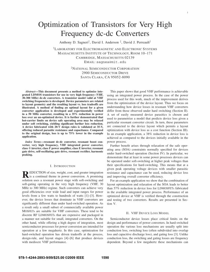
Fig. 1. Φ2 resonant boost converter with COSS and the external capacitanceCEXT explicitly drawn.
0 5 10 15 20 25 30 35 40 45−10
0
10
20
30
Time [ns]
Vol
tage
[V]
Class−Φ2 Converter Voltage and Current Waveforms
0 5 10 15 20 25 30 35 40 45−2
−1
0
1
2
3
Time [ns]
Cur
rent
[A]
DrainGate
ConductionDisplacement
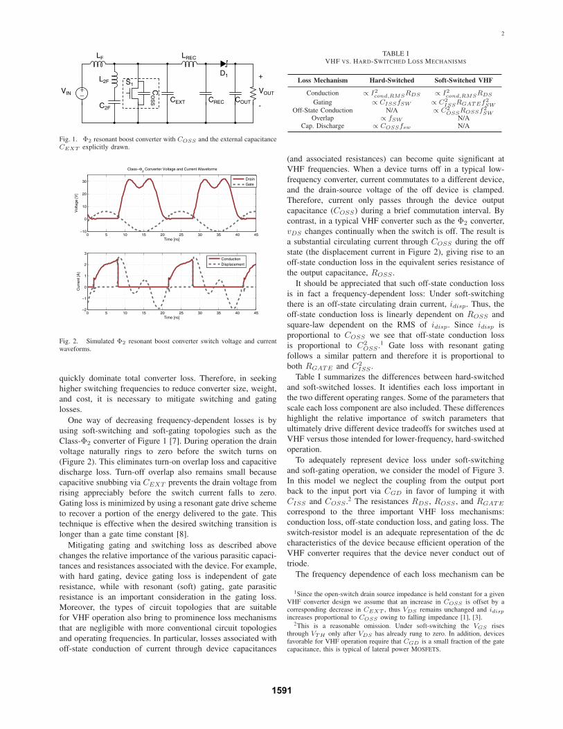
Fig. 2. Simulated Φ2 resonant boost converter switch voltage and currentwaveforms.
quickly dominate total converter loss. Therefore, in seekinghigher switching frequencies to reduce converter size, weight,and cost, it is necessary to mitigate switching and gatinglosses.
One way of decreasing frequency-dependent losses is byusing soft-switching and soft-gating topologies such as theClass-Φ2 converter of Figure 1 [7]. During operation the drainvoltage naturally rings to zero before the switch turns on(Figure 2). This eliminates turn-on overlap loss and capacitivedischarge loss. Turn-off overlap also remains small becausecapacitive snubbing via CEXT prevents the drain voltage fromrising appreciably before the switch current falls to zero.Gating loss is minimized by using a resonant gate drive schemeto recover a portion of the energy delivered to the gate. Thistechnique is effective when the desired switching transition islonger than a gate time constant [8].
Mitigating gating and switching loss as described abovechanges the relative importance of the various parasitic capaci-tances and resistances associated with the device. For example,with hard gating, device gating loss is independent of gateresistance, while with resonant (soft) gating, gate parasiticresistance is an important consideration in the gating loss.Moreover, the types of circuit topologies that are suitablefor VHF operation also bring to prominence loss mechanismsthat are negligible with more conventional circuit topologiesand operating frequencies. In particular, losses associated withoff-state conduction of current through device capacitances
TABLE IVHF VS. HARD-SWITCHED LOSS MECHANISMS
Loss Mechanism Hard-Switched Soft-Switched VHF
Conduction ∝ I2cond,RMSRDS ∝ I2
cond,RMSRDS
Gating ∝ CISSfSW ∝ C2ISSRGATEf2
SWOff-State Conduction N/A ∝ C2
OSSROSSf2SW
Overlap ∝ fSW N/ACap. Discharge ∝ COSSfsw N/A
(and associated resistances) can become quite significant atVHF frequencies. When a device turns off in a typical low-frequency converter, current commutates to a different device,and the drain-source voltage of the off device is clamped.Therefore, current only passes through the device outputcapacitance (COSS) during a brief commutation interval. Bycontrast, in a typical VHF converter such as the Φ2 converter,vDS changes continually when the switch is off. The result isa substantial circulating current through COSS during the offstate (the displacement current in Figure 2), giving rise to anoff-state conduction loss in the equivalent series resistance ofthe output capacitance, ROSS .
It should be appreciated that such off-state conduction lossis in fact a frequency-dependent loss: Under soft-switchingthere is an off-state circulating drain current, idisp. Thus, theoff-state conduction loss is linearly dependent on ROSS andsquare-law dependent on the RMS of idisp. Since idisp isproportional to COSS we see that off-state conduction lossis proportional to C2
OSS .1 Gate loss with resonant gatingfollows a similar pattern and therefore it is proportional toboth RGATE and C2
ISS .Table I summarizes the differences between hard-switched
and soft-switched losses. It identifies each loss important inthe two different operating ranges. Some of the parameters thatscale each loss component are also included. These differenceshighlight the relative importance of switch parameters thatultimately drive different device tradeoffs for switches used atVHF versus those intended for lower-frequency, hard-switchedoperation.
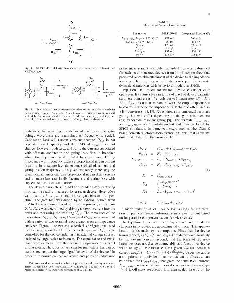
To adequately represent device loss under soft-switchingand soft-gating operation, we consider the model of Figure 3.In this model we neglect the coupling from the output portback to the input port via CGD in favor of lumping it withCISS and COSS .2 The resistances RDS , ROSS , and RGATE
correspond to the three important VHF loss mechanisms:conduction loss, off-state conduction loss, and gating loss. Theswitch-resistor model is an adequate representation of the dccharacteristics of the device because efficient operation of theVHF converter requires that the device never conduct out oftriode.
The frequency dependence of each loss mechanism can be
1Since the open-switch drain source impedance is held constant for a givenVHF converter design we assume that an increase in COSS is offset by acorresponding decrease in CEXT , thus VDS remains unchanged and idisp
increases proportional to COSS owing to falling impedance [1], [3].2This is a reasonable omission. Under soft-switching the VGS rises
through VTH only after VDS has already rung to zero. In addition, devicesfavorable for VHF operation require that CGD is a small fraction of the gatecapacitance, this is typical of lateral power MOSFETS.
1591
3
RDS
ICOND
IDISP
ROSS
COSS
CEXTRGATE
CISS
G
D
S
Fig. 3. MOSFET model with loss elements relevant under soft-switchedVHF operation
+−
+−
Dra
in B
ias
Gat
e B
ias
measurementport
CSHORT
RBIG
RBIG
+−
+−
RBIG
RBIG
Dra
in B
ias
Gat
e B
ias C
SH
OR
T measurementport
COSS = CDS + CGD CISS = CGS + CGD
Fig. 4. Two-terminal measurements are taken on an impedance analyzerto determine COSS , CISS , and CGD . CSHORT functions as an ac-shortat 1 MHz, the measurement frequency. The dc biases of VDS and VGS arecontrolled via external sources connected through large resistances.
understood by assuming the shapes of the drain- and gate-voltage waveforms are maintained as frequency is scaled.Conduction loss will remain constant because RDS is notdependent on frequency and the RMS of icond does notchange. However, both idisp and igate, the currents associatedwith off-state conduction and gating loss, flow in brancheswhere the impedance is dominated by capacitance. Fallingimpedance with frequency causes a proportional rise in currentresulting in a square-law dependence of displacement andgating loss on frequency. At a given frequency, increasing thebranch capacitances causes a proportional rise in their currentsand a square-law rise in displacement and gating loss withcapacitance, as discussed earlier.
The device parameters, in addition to adequately capturingloss, can be readily measured for a given device. Here, RDS
was taken as RDS−ON at the desired gate bias and temper-ature. The gate bias was driven by an external source from0 V to the maximum allowed VGS for the process, in this case20 V. RDS was determined by driving a known current into thedrain and measuring the resulting VDS . The remainder of theparameters, ROSS , RGATE , COSS , and CISS were measuredwith a series of two-terminal measurements on an impedanceanalyzer. Figure 4 shows the electrical configurations usedfor the measurements. DC bias of both VGS and VDS werecontrolled for the device under test via external voltage sourcesisolated by large series resistances. The capacitance and resis-tance were extracted from the measured impedance at each setof bias points. These results are small-signal values that can beused to reconstruct the large signal behavior of the device.3 Inorder to minimize contact resistance and parasitic inductance
3This assumes that the device is behaving quasistatically during operation.These models have been experimentally validated at frequencies up to 110MHz, in systems with important harmonics at 330 MHz.
TABLE IIMEASURED DEVICE PARAMETERS
Parameter MRF6S9060 Integrated LDMOS (F)
RDS−ON , VGS = 8 V, 25◦C 175 mΩ 200 mΩCOSS , VDS = 14.4 V 50 pF 132 pF
ROSS 170 mΩ 500 mΩCISS 110 pF 275 pF
RGATE 135 mΩ 1300 mΩPTOT 213 mW 915 mW
in the measurement assembly, individual jigs were fabricatedfor each set of measured devices from 10-mil copper sheet thatpermitted repeatable attachment of the device to the impedanceanalyzer. The resulting set of data points permits accuratedynamic simulations with behavioral models in SPICE.
Equation 1 is a model for the total device loss under VHFoperation. It captures loss in terms of a set of device parasiticparameters and a set of circuit derived parameters (K1, K2,K3). CEXT is added in parallel with the output capacitanceto control drain-source impedance, a technique often used inVHF converters [1], [7]. K3 is shown for sinusoidal resonantgating, but will differ depending on the gate drive scheme(e.g. trapezoidal resonant gating [9]). The currents, icond,RMS
and idisp,RMS are circuit-dependent and may be found bySPICE simulation. In some converters such as the Class-Ebased converters, closed-form expressions exist that allow thedirect calculation of the currents [10].
PTOT = Pcond + Pcond−off + Pgate
Pcond = K1 · RDS−ON
Pcond−off = K2 · ROSS,eq · C2OSS,eq
Pgate = K3 · RGATE,eq · C2ISS,eq
(1)
K1 = I2cond,RMS
K2 =(
Idisp,RMS
CTOT
)2
K3 = 2(π · Vgate,AC−pk · fSW )2
CTOT = COSS,eq + CEXT
This formulation of VHF device loss is useful for optimiza-tion. It predicts device performance in a given circuit basedon its parasitic component values (or vice versa).
In Equation 1 the non-linear capacitance and resistanceelements in the device are approximated as linear. This approx-imation holds under two assumptions: First, that the deviceterminal voltages VDS(t) and VGS(t) are determined primarilyby the external circuit. Second, that the form of the non-linearities does not change appreciably as a function of devicewidth or layout. For instance, for a given VDS(t) there is acurrent Idisp(t) = COSS(VDS(t)) · dVDS(t)
dt . Under the aboveassumptions an equivalent linear capacitance, COSS,eq, canbe defined for COSS(VDS) that gives the same RMS current,Idisp,RMS , as the non-linear capacitor under the drive voltageVDS(t). Off-state conduction loss then scales directly as the
1592
4
square of COSS,eq, which in turn scales approximately withdevice width.
A similar procedure is undertaken to determine ROSS .ROSS in an LDMOSFET is primarily a function of VDS
(though the dependence is typically weak). The desire isto find an equivalent resistance, ROSS,eq, that results inthe same power dissipation that ROSS exhibits under thedrive current Idisp(t). The power dissipation in ROSS is:Pdisp = 1
T
∫T
ROSS(VDS(t))I2disp(t)dt. Thus, ROSS,eq =
Pdisp/I2disp,RMS . Again, provided that VDS(t) is not a func-
tion of ROSS and the non-linearity is independent of devicewidth or layout, off-state conduction loss scales linearly withROSS,eq, which in turn scales inversely with device width.
In this paper we evaluate devices in the integrated process inthe context of a Class-Φ2 resonant boost converter switchingat 50 MHz. This design has VIN = 12 V, VOUT = 33 V, POUT
= 12 W, CTOT = 143 pF, idisp,RMS = 954 mA, icond,RMS =1040 mA, and vgate,AC−pk = 8 V. To establish a performancebaseline a discrete commercial RF LDMOSFET, the FreescaleMRF6S9060, is compared to a custom LDMOSFET fabricatedon an integrated BCD power process. Table II shows that thecommercial part dissipates only 213 mW, while the integrateddevice loses 915 mW in the example application.
III. LAYOUT OPTIMIZATION
A. Overview
The model presented in Section II provides a convenientgoal function to optimize a device within the context of aparticular circuit. In this case, we are looking to find anoptimal device for a resonant soft-switched VHF converter, theClass-Φ2 converter, in particular. Once the circuit dependentconstants have been selected, the device loss is only a functionof the device parasitic parameters RDS−ON , ROSS , RGATE ,COSS , and CISS . To affect a device optimization then requiresthat a device is changed in some way, the above parasiticparameters are computed relative to the change, and finallya new device loss is calculated from the model. The betterdevice has smaller total loss.
Process, design rule, or layout (or some combinationthereof) changes strongly affect the approach to an optimiza-tion method. While changing the process or design rules tobetter meet the requirements of VHF operation may offersubstantial gains in performance, the large number of vari-ables makes an optimization difficult and will come with asubstantial cost.
Layout changes within the design rules, on the other hand,are relatively easy to accomplish. Not only is the total numberof variables reduced, but the ability to rely on the scalability ofthe underlying device process means that the device parasiticparameters can be found largely through a set of simple scalinglaws. While a change in layout offers the least room fora performance improvement, most integrated power devicelayout has been accomplished with a very different set oflosses in mind. Typically the focus is on reducing specific on-resistance to minimize the total device area (and hence cost).The result is often a device with poor VHF characteristics,leaving much room for improvement.
FOXFOX GATE GATE
PWELL
PBODY NDRIFTNDRIFT
NBLP SUBSTRATE
N EPIN EPI
BULKSOURCE
DRAINDRAINN+ N+ N+ N+P+
Gate Poly
Drain
Source
Bulk
Contact
Field Termination
TOP VIEW
CROSS SECTION
wcell
wterm
wterm
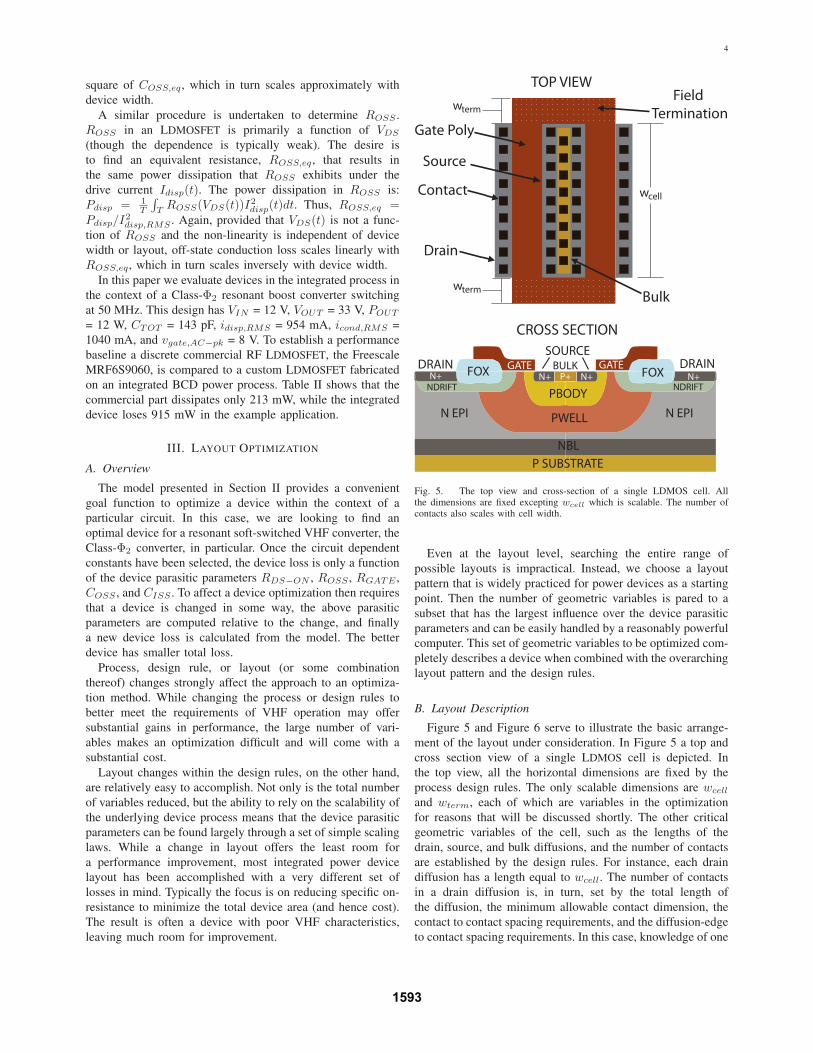
Fig. 5. The top view and cross-section of a single LDMOS cell. Allthe dimensions are fixed excepting wcell which is scalable. The number ofcontacts also scales with cell width.
Even at the layout level, searching the entire range ofpossible layouts is impractical. Instead, we choose a layoutpattern that is widely practiced for power devices as a startingpoint. Then the number of geometric variables is pared to asubset that has the largest influence over the device parasiticparameters and can be easily handled by a reasonably powerfulcomputer. This set of geometric variables to be optimized com-pletely describes a device when combined with the overarchinglayout pattern and the design rules.
B. Layout Description
Figure 5 and Figure 6 serve to illustrate the basic arrange-ment of the layout under consideration. In Figure 5 a top andcross section view of a single LDMOS cell is depicted. Inthe top view, all the horizontal dimensions are fixed by theprocess design rules. The only scalable dimensions are wcell
and wterm, each of which are variables in the optimizationfor reasons that will be discussed shortly. The other criticalgeometric variables of the cell, such as the lengths of thedrain, source, and bulk diffusions, and the number of contactsare established by the design rules. For instance, each draindiffusion has a length equal to wcell. The number of contactsin a drain diffusion is, in turn, set by the total length ofthe diffusion, the minimum allowable contact dimension, thecontact to contact spacing requirements, and the diffusion-edgeto contact spacing requirements. In this case, knowledge of one
1593
5
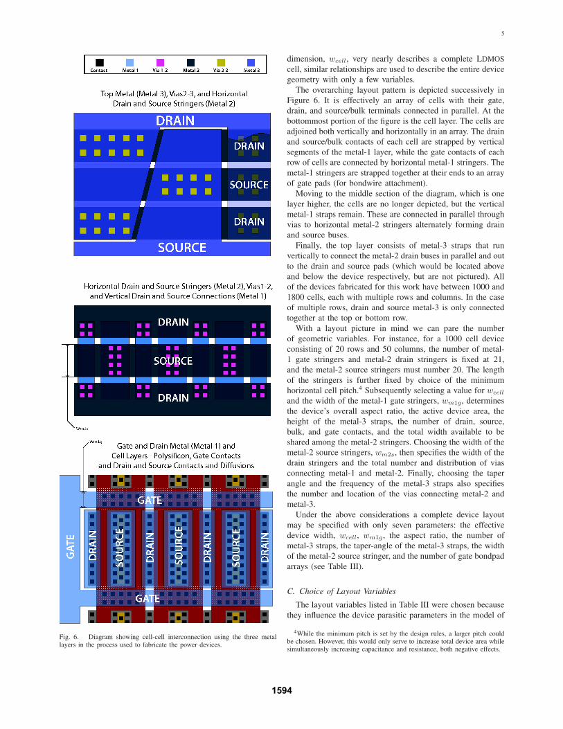
Fig. 6. Diagram showing cell-cell interconnection using the three metallayers in the process used to fabricate the power devices.
dimension, wcell, very nearly describes a complete LDMOScell, similar relationships are used to describe the entire devicegeometry with only a few variables.
The overarching layout pattern is depicted successively inFigure 6. It is effectively an array of cells with their gate,drain, and source/bulk terminals connected in parallel. At thebottommost portion of the figure is the cell layer. The cells areadjoined both vertically and horizontally in an array. The drainand source/bulk contacts of each cell are strapped by verticalsegments of the metal-1 layer, while the gate contacts of eachrow of cells are connected by horizontal metal-1 stringers. Themetal-1 stringers are strapped together at their ends to an arrayof gate pads (for bondwire attachment).
Moving to the middle section of the diagram, which is onelayer higher, the cells are no longer depicted, but the verticalmetal-1 straps remain. These are connected in parallel throughvias to horizontal metal-2 stringers alternately forming drainand source buses.
Finally, the top layer consists of metal-3 straps that runvertically to connect the metal-2 drain buses in parallel and outto the drain and source pads (which would be located aboveand below the device respectively, but are not pictured). Allof the devices fabricated for this work have between 1000 and1800 cells, each with multiple rows and columns. In the caseof multiple rows, drain and source metal-3 is only connectedtogether at the top or bottom row.
With a layout picture in mind we can pare the numberof geometric variables. For instance, for a 1000 cell deviceconsisting of 20 rows and 50 columns, the number of metal-1 gate stringers and metal-2 drain stringers is fixed at 21,and the metal-2 source stringers must number 20. The lengthof the stringers is further fixed by choice of the minimumhorizontal cell pitch.4 Subsequently selecting a value for wcell
and the width of the metal-1 gate stringers, wm1g , determinesthe device’s overall aspect ratio, the active device area, theheight of the metal-3 straps, the number of drain, source,bulk, and gate contacts, and the total width available to beshared among the metal-2 stringers. Choosing the width of themetal-2 source stringers, wm2s, then specifies the width of thedrain stringers and the total number and distribution of viasconnecting metal-1 and metal-2. Finally, choosing the taperangle and the frequency of the metal-3 straps also specifiesthe number and location of the vias connecting metal-2 andmetal-3.
Under the above considerations a complete device layoutmay be specified with only seven parameters: the effectivedevice width, wcell, wm1g , the aspect ratio, the number ofmetal-3 straps, the taper-angle of the metal-3 straps, the widthof the metal-2 source stringer, and the number of gate bondpadarrays (see Table III).
C. Choice of Layout Variables
The layout variables listed in Table III were chosen becausethey influence the device parasitic parameters in the model of
4While the minimum pitch is set by the design rules, a larger pitch couldbe chosen. However, this would only serve to increase total device area whilesimultaneously increasing capacitance and resistance, both negative effects.
1594
6
TABLE IIIOPTIMIZATION PARAMETERS
Parameter Importance to Device
Device Width Sets intrinsic RDS−ON , overall device sizeCell Width Affects RGATECISS and RDS−ONCOSS
Aspect Ratio Trades drain/source and gate metal losseswm1g Trades RGATE and COSS and CISS
# metal-3 cuts Drain-source metal resistanceangle metal-3 cuts Drain-source metal resistance
wm2s Drain-source metal resistance# gate bondpad arrays Trades RGATE and total device area
Section II, as well as describe a complete device. While otheraspects of the layout geometry could be used as optimizationvariables (eg. the number of vias connecting the metal-1 drainand source straps to the metal-2 drain and source stringers)they either have a weak effect on overall device performanceover reasonable variations of the parameter, or are alreadyconstrained by the selected set of variables. The followingdiscussion serves to illustrate the rationale behind the choiceof the optimization parameters.
The effective device width (referred to as ”Device Width”in Table III) has a strong influence over the device’s use-fulness for a particular application. It places a lower boundon RDS−ON , as this cannot be smaller than the intrinsicresistance. The same is true of the terminal capacitances,which must be at least as large as those of the cells withoutany surrounding metal. Since conduction loss will fall as theeffective width rises and the frequency dependent off-stateconduction and gating losses have the opposite behavior, thisparameter plays a central role in finding an optimal device.Beyond this, as the overall device area scales, the metallizationresistance will grow in importance.
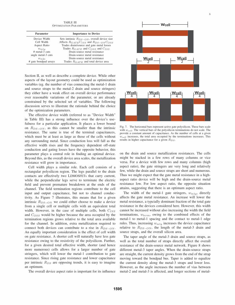
Cell width plays a similar role. Each cell consists of arectangular polysilicon region. The legs parallel to the draincontacts are effectively two LDMOSFETs that carry current,while the perpendicular legs serve to terminate the electricfield and prevent premature breakdown at the ends of thechannel. The field termination regions contribute to the cellinput and output capacitance, but not to channel conduc-tivity. As Figure 7 illustrates, this means that for a givenintrinsic RDS−ON we could either choose to make a devicefrom a single cell or multiple cells with an equivalent totalwidth. However, in the case of multiple cells, both CISS
and COSS would be higher because the area occupied by thetermination regions grows relative to the total area availablefor the channel. In addition, extra metallization required toconnect both devices can contribute to a rise in RDS−ON .An equally important consideration is the effect of cell widthon gate resistance. A shorter cell will naturally have less gateresistance owing to the resistivity of the polysilicon. Further,for a given desired total effective width, shorter (and hencemore numerous) cells allows for a larger number of gatestringers, which will lower the metal-1 contribution to gateresistance. Since rising gate resistance and lower capacitanceper intrinsic RDS are opposing trends, it is easy to imaginean optimum.
The overall device aspect ratio is important for its influence
wcell
wcell2
wcell2
wcell4
wcell4
wcell4
wcell4
Fig. 7. The horizontal bars represent active gate polysilicon. These bars scalewith wcell. The vertical bars of the polysilicon terminations do not scale. Theprovide a constant amount of capacitance. As the number of cells at a givenwcell increases, the total area occupied by the terminations increases. Thisresults in higher capacitance for a given RDS .
on the drain and source metallization resistances. The cellsmight be stacked in a few rows of many columns or viceversa. For a device with few rows and many columns (highaspect ratio), the gate stringers are very long and relativelyfew, while the drain and source straps are short and numerous.Thus we might expect that the gate metal resistance in a high-aspect ratio device will be high and the drain-source metalresistance low. For low aspect ratio, the opposite situationattains, suggesting that there is an optimum aspect ratio.
The width of the metal-1 gate stringers, wm1g , directlyaffects the gate metal resistance. An increase will lower themetal resistance, a typcially dominant fraction of the total gateresistance in the devices considered here. However, this widthcannot be increased without also increasing the width the fieldterminations, wterm, owing to the combined effects of themetal-1 to metal-1 spacing and the contact to metal-1 edgerules. Thus, increasing wm1g increases the device capacitancerelative to RDS−ON , the length of the metal-3 drain andsource straps, and the overall silicon area.
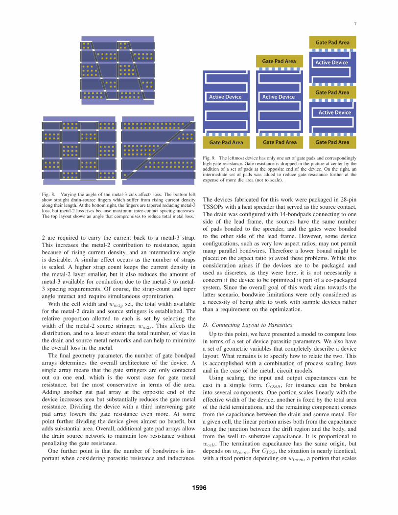
The taper angle of the metal-3 drain and source straps, aswell as the total number of straps directly affect the overallresistance of the drain-source metal network. Figure 8 showsdifferent metal-3 taper angles. When the drain-source strapsare straight, the current density grows from the end of the strapmoving toward the bondpad bus. Taper is added to equalizethe current density along the metal-3 straps and lower loss.However, as the angle increases the number of vias betweenmetal-2 and metal-3 is affected, and longer sections of metal-
1595
7
Fig. 8. Varying the angle of the metal-3 cuts affects loss. The bottom leftshow straight drain-source fingers which suffer from rising current densityalong their length. At the bottom right, the fingers are tapered reducing metal-3loss, but metal-2 loss rises because maximum inter-contact spacing increases.The top layout shows an angle that compromises to reduce total metal loss.
2 are required to carry the current back to a metal-3 strap.This increases the metal-2 contribution to resistance, againbecause of rising current density, and an intermediate angleis desirable. A similar effect occurs as the number of strapsis scaled. A higher strap count keeps the current density inthe metal-2 layer smaller, but it also reduces the amount ofmetal-3 available for conduction due to the metal-3 to metal-3 spacing requirements. Of course, the strap-count and taperangle interact and require simultaneous optimization.
With the cell width and wm1g set, the total width availablefor the metal-2 drain and source stringers is established. Therelative proportion allotted to each is set by selecting thewidth of the metal-2 source stringer, wm2s. This affects thedistribution, and to a lesser extent the total number, of vias inthe drain and source metal networks and can help to minimizethe overall loss in the metal.
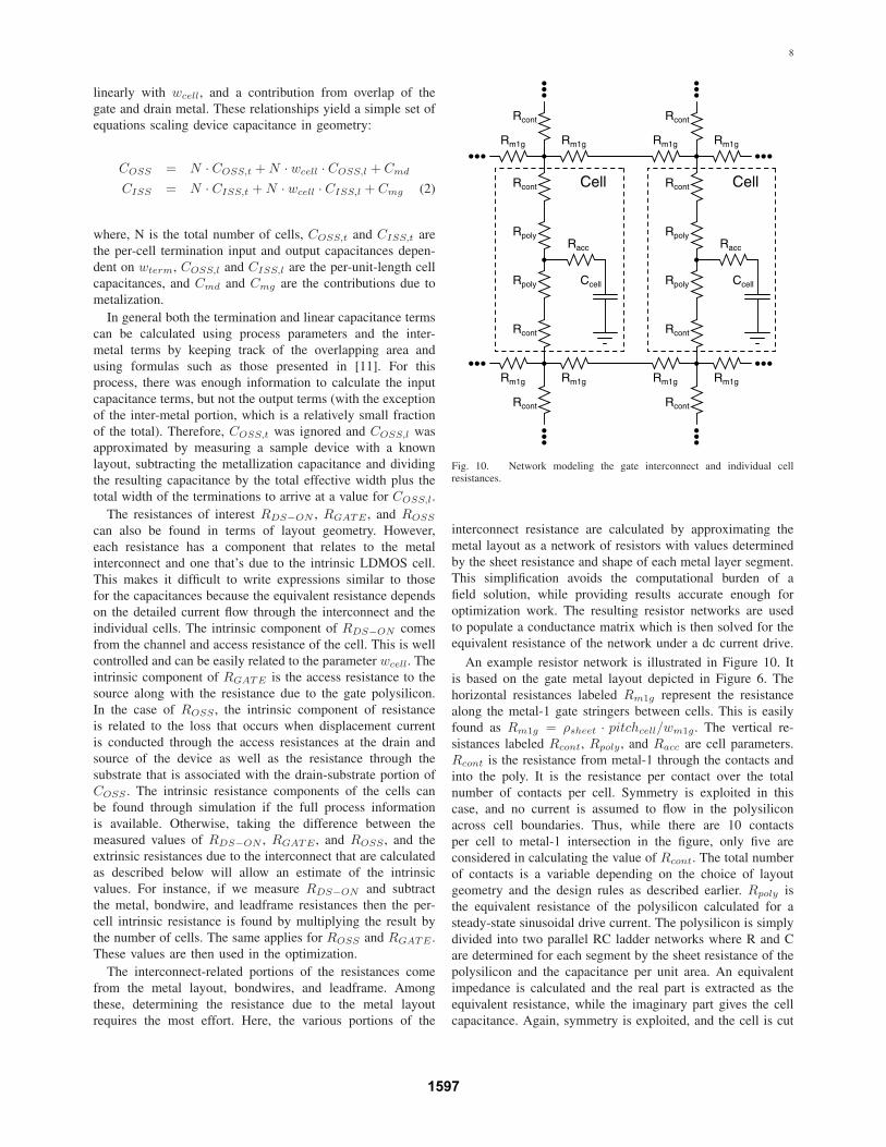
The final geometry parameter, the number of gate bondpadarrays determines the overall architecture of the device. Asingle array means that the gate stringers are only contactedout on one end, which is the worst case for gate metalresistance, but the most conservative in terms of die area.Adding another gat pad array at the opposite end of thedevice increases area but substantially reduces the gate metalresistance. Dividing the device with a third intervening gatepad array lowers the gate resistance even more. At somepoint further dividing the device gives almost no benefit, butadds substantial area. Overall, additional gate pad arrays allowthe drain source network to maintain low resistance withoutpenalizing the gate resistance.
One further point is that the number of bondwires is im-portant when considering parasitic resistance and inductance.
Gate Pad Area
Gate Pad AreaGate Pad Area Gate Pad Area
Gate Pad Area
Gate Pad AreaActive Device Active Device
Active Device
Active Device
Fig. 9. The leftmost device has only one set of gate pads and correspondinglyhigh gate resistance. Gate resistance is dropped in the picture at center by theaddition of a set of pads at the opposite end of the device. On the right, anintermediate set of pads was added to reduce gate resistance further at theexpense of more die area (not to scale).
The devices fabricated for this work were packaged in 28-pinTSSOPs with a heat spreader that served as the source contact.The drain was configured with 14-bondpads connecting to oneside of the lead frame, the sources have the same numberof pads bonded to the spreader, and the gates were bondedto the other side of the lead frame. However, some deviceconfigurations, such as very low aspect ratios, may not permitmany parallel bondwires. Therefore a lower bound might beplaced on the aspect ratio to avoid these problems. While thisconsideration arises if the devices are to be packaged andused as discretes, as they were here, it is not necessarily aconcern if the device to be optimized is part of a co-packagedsystem. Since the overall goal of this work aims towards thelatter scenario, bondwire limitations were only considered asa necessity of being able to work with sample devices ratherthan a requirement on the optimization.
D. Connecting Layout to Parasitics
Up to this point, we have presented a model to compute lossin terms of a set of device parasitic parameters. We also havea set of geometric variables that completely describe a devicelayout. What remains is to specify how to relate the two. Thisis accomplished with a combination of process scaling lawsand in the case of the metal, circuit models.
Using scaling, the input and output capacitances can becast in a simple form. COSS , for instance can be brokeninto several components. One portion scales linearly with theeffective width of the device, another is fixed by the total areaof the field terminations, and the remaining component comesfrom the capacitance between the drain and source metal. Fora given cell, the linear portion arises both from the capacitancealong the junction between the drift region and the body, andfrom the well to substrate capacitance. It is proportional towcell. The termination capacitance has the same origin, butdepends on wterm. For CISS , the situation is nearly identical,with a fixed portion depending on wterm, a portion that scales
1596
8
linearly with wcell, and a contribution from overlap of thegate and drain metal. These relationships yield a simple set ofequations scaling device capacitance in geometry:
COSS = N · COSS,t + N · wcell · COSS,l + Cmd
CISS = N · CISS,t + N · wcell · CISS,l + Cmg (2)
where, N is the total number of cells, COSS,t and CISS,t arethe per-cell termination input and output capacitances depen-dent on wterm, COSS,l and CISS,l are the per-unit-length cellcapacitances, and Cmd and Cmg are the contributions due tometalization.
In general both the termination and linear capacitance termscan be calculated using process parameters and the inter-metal terms by keeping track of the overlapping area andusing formulas such as those presented in [11]. For thisprocess, there was enough information to calculate the inputcapacitance terms, but not the output terms (with the exceptionof the inter-metal portion, which is a relatively small fractionof the total). Therefore, COSS,t was ignored and COSS,l wasapproximated by measuring a sample device with a knownlayout, subtracting the metallization capacitance and dividingthe resulting capacitance by the total effective width plus thetotal width of the terminations to arrive at a value for COSS,l.
The resistances of interest RDS−ON , RGATE , and ROSS
can also be found in terms of layout geometry. However,each resistance has a component that relates to the metalinterconnect and one that’s due to the intrinsic LDMOS cell.This makes it difficult to write expressions similar to thosefor the capacitances because the equivalent resistance dependson the detailed current flow through the interconnect and theindividual cells. The intrinsic component of RDS−ON comesfrom the channel and access resistance of the cell. This is wellcontrolled and can be easily related to the parameter wcell. Theintrinsic component of RGATE is the access resistance to thesource along with the resistance due to the gate polysilicon.In the case of ROSS , the intrinsic component of resistanceis related to the loss that occurs when displacement currentis conducted through the access resistances at the drain andsource of the device as well as the resistance through thesubstrate that is associated with the drain-substrate portion ofCOSS . The intrinsic resistance components of the cells canbe found through simulation if the full process informationis available. Otherwise, taking the difference between themeasured values of RDS−ON , RGATE , and ROSS , and theextrinsic resistances due to the interconnect that are calculatedas described below will allow an estimate of the intrinsicvalues. For instance, if we measure RDS−ON and subtractthe metal, bondwire, and leadframe resistances then the per-cell intrinsic resistance is found by multiplying the result bythe number of cells. The same applies for ROSS and RGATE .These values are then used in the optimization.
The interconnect-related portions of the resistances comefrom the metal layout, bondwires, and leadframe. Amongthese, determining the resistance due to the metal layoutrequires the most effort. Here, the various portions of the
Rm1g
Rcont
RpolyRacc
CcellRpoly
Rcont
Rcont
Rcont
Rm1g
Rm1g Rm1g
Cell
Rm1g
Rcont
RpolyRacc
CcellRpoly
Rcont
Rcont
Rcont
Rm1g
Rm1g Rm1g
Cell
Fig. 10. Network modeling the gate interconnect and individual cellresistances.
interconnect resistance are calculated by approximating themetal layout as a network of resistors with values determinedby the sheet resistance and shape of each metal layer segment.This simplification avoids the computational burden of afield solution, while providing results accurate enough foroptimization work. The resulting resistor networks are usedto populate a conductance matrix which is then solved for theequivalent resistance of the network under a dc current drive.
An example resistor network is illustrated in Figure 10. Itis based on the gate metal layout depicted in Figure 6. Thehorizontal resistances labeled Rm1g represent the resistancealong the metal-1 gate stringers between cells. This is easilyfound as Rm1g = ρsheet · pitchcell/wm1g . The vertical re-sistances labeled Rcont, Rpoly , and Racc are cell parameters.Rcont is the resistance from metal-1 through the contacts andinto the poly. It is the resistance per contact over the totalnumber of contacts per cell. Symmetry is exploited in thiscase, and no current is assumed to flow in the polysiliconacross cell boundaries. Thus, while there are 10 contactsper cell to metal-1 intersection in the figure, only five areconsidered in calculating the value of Rcont. The total numberof contacts is a variable depending on the choice of layoutgeometry and the design rules as described earlier. Rpoly isthe equivalent resistance of the polysilicon calculated for asteady-state sinusoidal drive current. The polysilicon is simplydivided into two parallel RC ladder networks where R and Care determined for each segment by the sheet resistance of thepolysilicon and the capacitance per unit area. An equivalentimpedance is calculated and the real part is extracted as theequivalent resistance, while the imaginary part gives the cellcapacitance. Again, symmetry is exploited, and the cell is cut
1597
9
in half to find Rpoly from either direction. Since the cellconsists of two legs, Rpoly is halved, and Ccell is doubled.Finally, Racc is the access resistance from the source side ofthe cell.
Once the resistor network values are determined, a con-ductance matrix is populated and solved for the equivalentimpedance of the entire gate network, the real part being theresistance. RGATE is then found as the resistance calculatedfrom the resistor network plus the resistance of the bondwiresand leadframe.
A similar procedure is performed for the drain-sourcenetwork. The resulting network is more complicated, butindividual resistance values within the network are easilyrelated back to simple geometric parameters such as cell-pitch, width of the metal-2 stringers, and the number of viasconnecting adjacent layers of metal. In order to capture thedependence of the drain and source metal resistance on thecut angle of metal-3, it is necessary to represent these sheetsof metal as a 2 dimensional grid of resistors. The granularitywith which the network is divided into discrete resistances isarbitrary, but a fine mesh is computationally challenging anda course mesh is not accurate enough. It was found that onenode per cell is adequate for the optimization performed here.
The final network includes both drain and source metalas well as the intrinsic cell resistances. This allows forthe calculation of an equivalent drain-source resistance thatincludes the effects of an asymmetric layout. RDS−ON isfound by solving the nodal equations for a dc current drive atthe drain with the source shorted to ground. During converteroperation, current is either flowing through the interconnectnetwork and the channel, or the interconnect network and theoutput capacitance. Therefore, ROSS is found by the samemethod as RDS−ON , with the exception that the resistorsconnecting the drain and source networks are substituted bythe intrinsic value of ROSS , rather than RDS .
E. Optimization
With the means to connect layout geometry to device loss,optimization is a relatively straightforward task. Since the setof geometry variables was kept small, a few thousand layoutscan be evaluated in the space of an hour. At this rate, a bruteforce search of the layout space is easily accomplished, avoid-ing the pitfalls common to algorithms such as gradient descent.The primary challenge to setting up such an optimization iswriting code that correctly accounts for the design rules andtraps for non-physical situations as the various optimizationparameters are varied.
A MATLAB script was created to perform the optimization.It takes various process parameters such as the resistivity ofthe metal layers and the intrinsic resistances and capacitancesas inputs along with the circuit constants that represent theapplication the device will be optimized for. The code beginsby loading the process design rules. It then sequentially per-mutes the seven geometry variables of Table III. For each set ofvariables, the code uses the design rules to arrive at a completegeometry, including the cell pitch, metal dimensions, contactand via descriptions, bondpad locations, and the various details
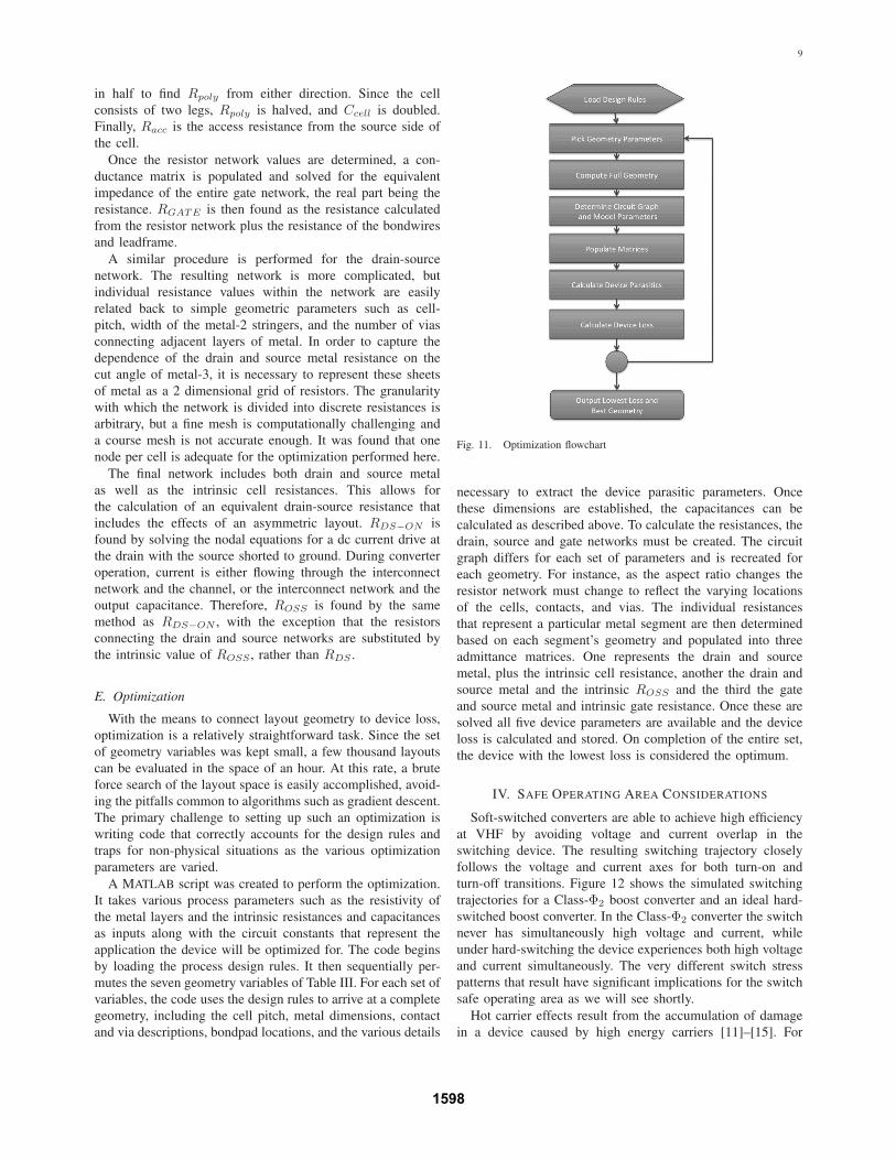
Fig. 11. Optimization flowchart
necessary to extract the device parasitic parameters. Oncethese dimensions are established, the capacitances can becalculated as described above. To calculate the resistances, thedrain, source and gate networks must be created. The circuitgraph differs for each set of parameters and is recreated foreach geometry. For instance, as the aspect ratio changes theresistor network must change to reflect the varying locationsof the cells, contacts, and vias. The individual resistancesthat represent a particular metal segment are then determinedbased on each segment’s geometry and populated into threeadmittance matrices. One represents the drain and sourcemetal, plus the intrinsic cell resistance, another the drain andsource metal and the intrinsic ROSS and the third the gateand source metal and intrinsic gate resistance. Once these aresolved all five device parameters are available and the deviceloss is calculated and stored. On completion of the entire set,the device with the lowest loss is considered the optimum.
IV. SAFE OPERATING AREA CONSIDERATIONS
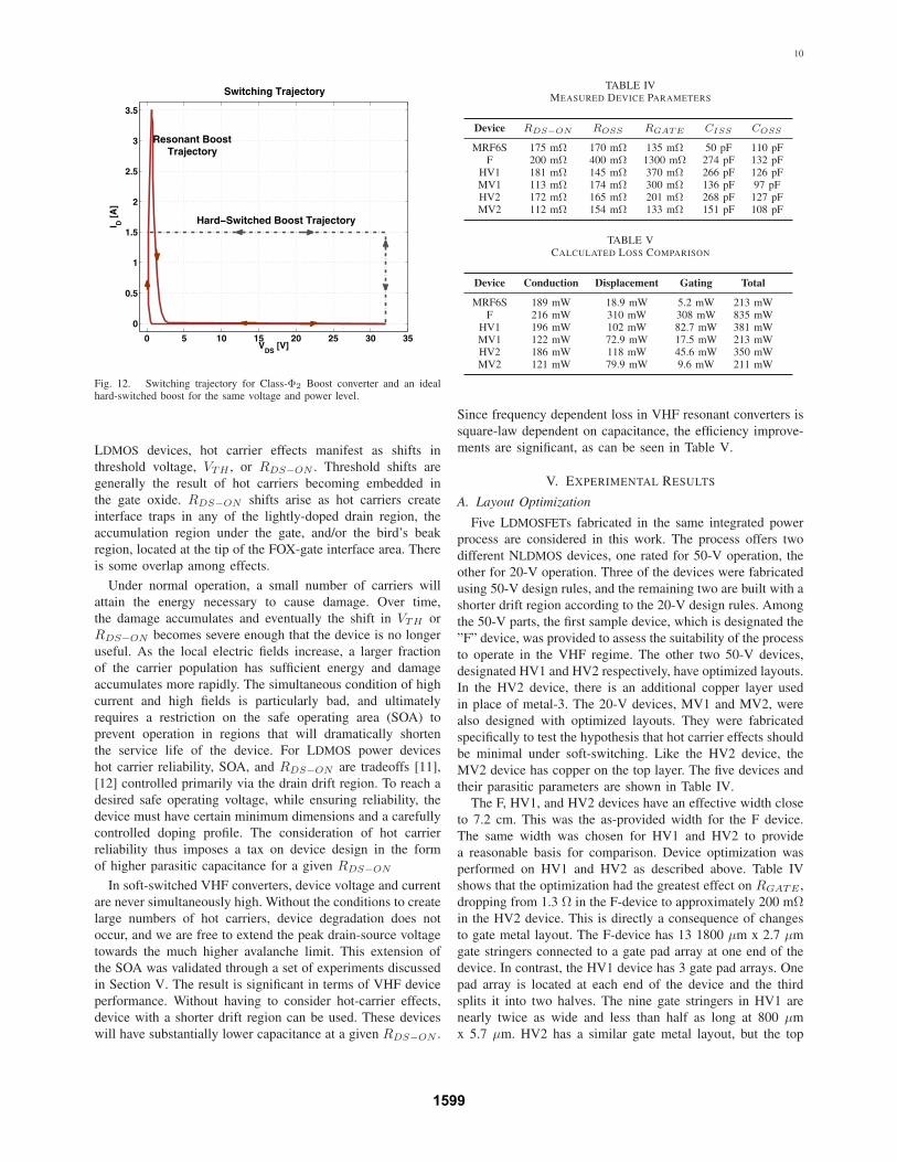
Soft-switched converters are able to achieve high efficiencyat VHF by avoiding voltage and current overlap in theswitching device. The resulting switching trajectory closelyfollows the voltage and current axes for both turn-on andturn-off transitions. Figure 12 shows the simulated switchingtrajectories for a Class-Φ2 boost converter and an ideal hard-switched boost converter. In the Class-Φ2 converter the switchnever has simultaneously high voltage and current, whileunder hard-switching the device experiences both high voltageand current simultaneously. The very different switch stresspatterns that result have significant implications for the switchsafe operating area as we will see shortly.
Hot carrier effects result from the accumulation of damagein a device caused by high energy carriers [11]–[15]. For
1598
10
0 5 10 15 20 25 30 35
0
0.5
1
1.5
2
2.5
3
3.5
VDS
[V]
I D [
A]
Switching Trajectory
Resonant BoostTrajectory
Hard−Switched Boost Trajectory
Fig. 12. Switching trajectory for Class-Φ2 Boost converter and an idealhard-switched boost for the same voltage and power level.
LDMOS devices, hot carrier effects manifest as shifts inthreshold voltage, VTH , or RDS−ON . Threshold shifts aregenerally the result of hot carriers becoming embedded inthe gate oxide. RDS−ON shifts arise as hot carriers createinterface traps in any of the lightly-doped drain region, theaccumulation region under the gate, and/or the bird’s beakregion, located at the tip of the FOX-gate interface area. Thereis some overlap among effects.
Under normal operation, a small number of carriers willattain the energy necessary to cause damage. Over time,the damage accumulates and eventually the shift in VTH orRDS−ON becomes severe enough that the device is no longeruseful. As the local electric fields increase, a larger fractionof the carrier population has sufficient energy and damageaccumulates more rapidly. The simultaneous condition of highcurrent and high fields is particularly bad, and ultimatelyrequires a restriction on the safe operating area (SOA) toprevent operation in regions that will dramatically shortenthe service life of the device. For LDMOS power deviceshot carrier reliability, SOA, and RDS−ON are tradeoffs [11],[12] controlled primarily via the drain drift region. To reach adesired safe operating voltage, while ensuring reliability, thedevice must have certain minimum dimensions and a carefullycontrolled doping profile. The consideration of hot carrierreliability thus imposes a tax on device design in the formof higher parasitic capacitance for a given RDS−ON
In soft-switched VHF converters, device voltage and currentare never simultaneously high. Without the conditions to createlarge numbers of hot carriers, device degradation does notoccur, and we are free to extend the peak drain-source voltagetowards the much higher avalanche limit. This extension ofthe SOA was validated through a set of experiments discussedin Section V. The result is significant in terms of VHF deviceperformance. Without having to consider hot-carrier effects,device with a shorter drift region can be used. These deviceswill have substantially lower capacitance at a given RDS−ON .
TABLE IVMEASURED DEVICE PARAMETERS
Device RDS−ON ROSS RGATE CISS COSS
MRF6S 175 mΩ 170 mΩ 135 mΩ 50 pF 110 pFF 200 mΩ 400 mΩ 1300 mΩ 274 pF 132 pF
HV1 181 mΩ 145 mΩ 370 mΩ 266 pF 126 pFMV1 113 mΩ 174 mΩ 300 mΩ 136 pF 97 pFHV2 172 mΩ 165 mΩ 201 mΩ 268 pF 127 pFMV2 112 mΩ 154 mΩ 133 mΩ 151 pF 108 pF
TABLE VCALCULATED LOSS COMPARISON
Device Conduction Displacement Gating Total
MRF6S 189 mW 18.9 mW 5.2 mW 213 mWF 216 mW 310 mW 308 mW 835 mW
HV1 196 mW 102 mW 82.7 mW 381 mWMV1 122 mW 72.9 mW 17.5 mW 213 mWHV2 186 mW 118 mW 45.6 mW 350 mWMV2 121 mW 79.9 mW 9.6 mW 211 mW
Since frequency dependent loss in VHF resonant converters issquare-law dependent on capacitance, the efficiency improve-ments are significant, as can be seen in Table V.
V. EXPERIMENTAL RESULTS
A. Layout Optimization
Five LDMOSFETs fabricated in the same integrated powerprocess are considered in this work. The process offers twodifferent NLDMOS devices, one rated for 50-V operation, theother for 20-V operation. Three of the devices were fabricatedusing 50-V design rules, and the remaining two are built with ashorter drift region according to the 20-V design rules. Amongthe 50-V parts, the first sample device, which is designated the”F” device, was provided to assess the suitability of the processto operate in the VHF regime. The other two 50-V devices,designated HV1 and HV2 respectively, have optimized layouts.In the HV2 device, there is an additional copper layer usedin place of metal-3. The 20-V devices, MV1 and MV2, werealso designed with optimized layouts. They were fabricatedspecifically to test the hypothesis that hot carrier effects shouldbe minimal under soft-switching. Like the HV2 device, theMV2 device has copper on the top layer. The five devices andtheir parasitic parameters are shown in Table IV.
The F, HV1, and HV2 devices have an effective width closeto 7.2 cm. This was the as-provided width for the F device.The same width was chosen for HV1 and HV2 to providea reasonable basis for comparison. Device optimization wasperformed on HV1 and HV2 as described above. Table IVshows that the optimization had the greatest effect on RGATE ,dropping from 1.3 Ω in the F-device to approximately 200 mΩin the HV2 device. This is directly a consequence of changesto gate metal layout. The F-device has 13 1800 μm x 2.7 μmgate stringers connected to a gate pad array at one end of thedevice. In contrast, the HV1 device has 3 gate pad arrays. Onepad array is located at each end of the device and the thirdsplits it into two halves. The nine gate stringers in HV1 arenearly twice as wide and less than half as long at 800 μmx 5.7 μm. HV2 has a similar gate metal layout, but the top
1599
11
15 20 25 30 35
1110
1120
1130
1140
Run Voltage [V]
Thr
esho
ld V
olta
ge [m
V]
20V integrated device after 100 hours at each run voltage
15 20 25 30 35152
154
156
158
160
162
Run Voltage [V]
RD
S−
ON
[mΩ
]
Fig. 13. The shifts in VTH and RDS−ON are well within the establishedtesting criteria.
drain-source metal is copper allowing the device to be muchmore square (F and HV1 are about 500 μm x 2 mm, whereas HV2 is about 1.1 mm x 1.3 mm). This doubles the numberof gate stringers dropping the total gate resistance to 201 mΩ.
The HV1 and HV2 devices also have 35 μm cells in contrastwith the F device’s 25 μm cells. This slightly reduces inputand output capacitance, which also shows up in Table IV. Itadditionally allows for wider metal-2 conductors (the largestsource of resistance in the drain-source metal for these highaspect ratio devices) in the drain source path. In conjunctionwith a somewhat shallower metal-3 angle in the HV1 device, amodest reduction in metal resistance was achieved, contribut-ing to a lower RDS−ON . In the HV2 device, metal-2 andmetal-3 are paralleled to further reduce the contribution fromthe drain and source stringers, and copper is used in place ofmetal-3 for the topmost layer.
The overall reduction in loss among the 50-V devices fromlayout optimization alone is substantial, as Table V shows.The losses are calculated using the same example converteras in Section II. It should be noted that the F device is not atypical example of a power device in this process. The choiceof high aspect ratio and short finger length was an initialattempt to achieve a device compatible with VHF operationfor testing purposes. That fact that a full optimization alloweda further improvement of the RDS−ON · COUT product isencouraging. After layout optimization alone, the HV deviceshave a reduction in loss of up to 55%.
B. Safe Operating Area
The MV1 and MV2 devices provide even better perfor-mance. These take advantage of 20-V design rules that allowfor a shorter drift region and lower specific on resistance.When these devices are compared to the discrete MRF6S9060,in the example 50-MHz Φ2 converter, they achieve the sametotal loss. This means that in the intended application at 50-MHz the integrated process can achieve parity with a discretedevice picked from among the best available.
0 200 400 600 800 1000
1110
1120
1130
1140
Run Time at 35 V [Hours]
Thr
esho
ld V
olta
ge [m
V]
20V MV1 device VT and R
DS−ON vs. run time at 35 V
0 200 400 600 800 1000152
154
156
158
160
162
Run Time at 35 V [Hours]
RD
S−
ON
[mΩ
]
Fig. 14. After 1000 hours of operation at 35V, the 20V MV1 device has atotal VTH shift of around 20mV, and about a 4% change in RDS−ON . Theallowable maximums are 100mV and 10%, respectively.
While improved performance is expected from a devicewith a lower voltage rating, the point of interest is that itcan be used in this application at all. In the experimentalconverters constructed to test these devices, the peak drainvoltage attained during operation is 35 V, a 75% increase overthe rated voltage of the MV1 and MV2 devices. As discussedin Section IV, the mechanism that underscores this ability is aswitching trajectory that never has simultaneous high voltageand current. This minimizes hot carrier effects, allowing theMV1 and MV2 devices to be used at peak voltages closer totheir avalanche voltage which is around 40 V.
To assess hot carrier reliability in this process under soft-switching we used the manufacturer’s hot carrier reliabilitycriteria. These require the device to run for 1 year at 10% dutyratio. To meet standards RDS−ON must shift by 10%, or less,and VTH by 100 mV, or less. In order to evaluate our devices,we ran the device in a Class-Φ2 resonant boost converter (seeFigure 15 and Table VI) at successively higher voltages for100 hour periods. The test started with a peak VDS of 15 V.Once 35 V was reached, the converter was allowed to run foran additional 1000 hours. In terms of the manufacturer test thisis more than adequate. Hot carrier damage occurs primarilyat switching transitions. Since the test converter ran at 50MHz, the total number of transitions substantially exceedswhat would be expected of a hard-switched converter.
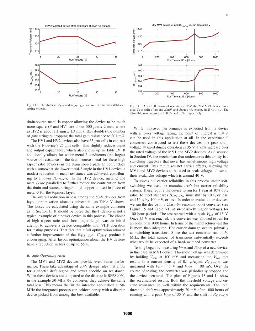
Testing began by measuring VTH and RDS of a new device,in this case an MV1 device. Threshold voltage was determinedby holding VDS at 100 mV and measuring the VGS thatresults in a current density of 0.1 μA/μm. RDS−ON wasmeasured with VGS = 5 V and VDS = 100 mV. Over thecourse of testing, the converter was periodically stopped andthe device measured. The plots of Figures 13 and 14 showthe accumulated results. Both the threshold voltage and on-state resistance lie well within the requirements. The totalthreshold shift was approximately 20 mV after 1000 hours ofrunning with a peak VDS of 35 V, and the shift in RDS−ON
1600
12
was on the order of 4%. At 712 hours the input voltage tothe converter was nearly doubled, stressing the devices andproducing the steep rise in RDS−ON demarcated by the blackline in figure 14. Even with this additional stress, the totalshift is well within the evaluation criteria.
As a control, a hard-switched boost converter was designedaround an MV1 device to operate at the same voltage andpower level. The converter was then connected to an electronicload so that average current through the switch could bemaintained near 1.75 A, identical to the Φ2 resonant boostconverter when the peak VDS is 35 V. After an initial runof 100 hours with a peak drain source voltage of 20 V, littlechange in VTH or RDS−ON was observed. After the initialrun, the converter was then operated for 5 minute intervals atsuccessively higher peak VDS . This short interval was pickedbecause shifts were expected to appear rapidly as the devicevoltage increased outside of the SOA. At a peak VDS of 30V, no changes were evident. Upon increasing the peak drain-source voltage to 35 V, the same voltage at which another MV1device operated for over 1000 hours under soft-switching, thehard-switched device failed in 18 seconds.
The soft-switching trajectory that permits SOA extensionmay not exist in the Φ2 converter (or other VHF resonantconverters) if the converter is not operating in steady state. Forexample, a typical method of controlling VHF soft-switchingconverters is full on-off modulation. [9]. During the start-upand shut-down transients, the switching trajectory will notalways closely follow the voltage and current axes. Duringthese periods, it is necessary that the trajectory does not leavethe SOA defined for hard-switched converters, or significanthot carrier damage could occur. To assess the feasibility ofoperating an SOA-extended 20-V switch under these condi-tions, a Φ2 converter was configured for modulation. Undermodulation, the entire power stage is turned on and off at afrequency far below the switching frequency. In this case, a 50-kHz signal was used to modulate a 50-MHz converter. Afterrunning the converter with a peak VDS of 35 V for 120 hours,there was no measurable shift in either VTH or RDS−ON .
The benefits of extending SOA are clearly delineated inTables IV and V. The MV devices enjoy a 76% reductionin loss over the original un-optimized F device. The primarybenefit comes from the lower specific RDS−ON . This resultsin substantially lower capacitance and devices with an activearea roughly 20% smaller than the HV versions. The smallerdimensions also reduce the total interconnect length andthe MV2 device, which has copper top metal and a smallaspect ratio posts the lowest RGATE , 133 mΩ. While thelarger capacitances of the integrated devices over the discreteexample (MRF6S9060) means that they won’t scale as wellin frequency, 50 MHz is sufficiently high to make converterswith co-packaged energy storage a possibility.
C. Converters
To illustrate the gains from device optimization and SOAextension, two 50-MHz Class-Φ2 resonant boost converterswere constructed. The details are found in Table VI. Oneconverter uses an un-optimized F device. The other uses the
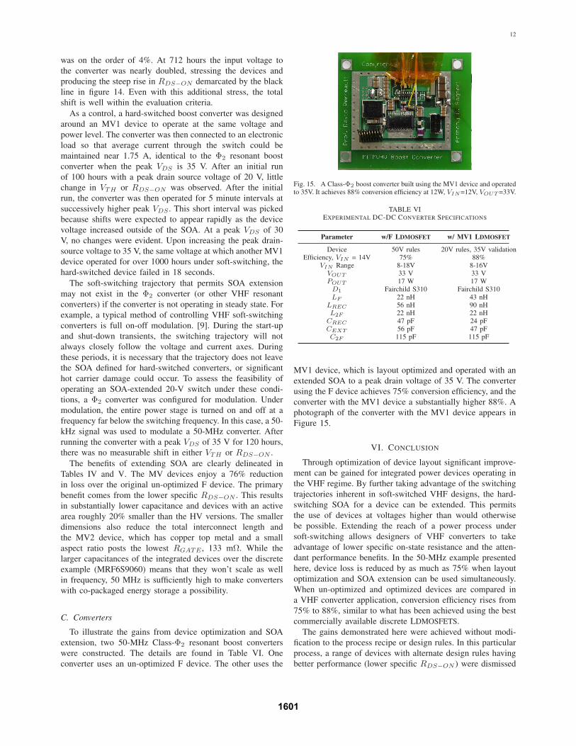
Fig. 15. A Class-Φ2 boost converter built using the MV1 device and operatedto 35V. It achieves 88% conversion efficiency at 12W, VIN =12V, VOUT =33V.
TABLE VIEXPERIMENTAL DC-DC CONVERTER SPECIFICATIONS
Parameter w/F LDMOSFET w/ MV1 LDMOSFET
Device 50V rules 20V rules, 35V validationEfficiency, VIN = 14V 75% 88%
VIN Range 8-18V 8-16VVOUT 33 V 33 VPOUT 17 W 17 W
D1 Fairchild S310 Fairchild S310LF 22 nH 43 nH
LREC 56 nH 90 nHL2F 22 nH 22 nH
CREC 47 pF 24 pFCEXT 56 pF 47 pFC2F 115 pF 115 pF
MV1 device, which is layout optimized and operated with anextended SOA to a peak drain voltage of 35 V. The converterusing the F device achieves 75% conversion efficiency, and theconverter with the MV1 device a substantially higher 88%. Aphotograph of the converter with the MV1 device appears inFigure 15.
VI. CONCLUSION
Through optimization of device layout significant improve-ment can be gained for integrated power devices operating inthe VHF regime. By further taking advantage of the switchingtrajectories inherent in soft-switched VHF designs, the hard-switching SOA for a device can be extended. This permitsthe use of devices at voltages higher than would otherwisebe possible. Extending the reach of a power process undersoft-switching allows designers of VHF converters to takeadvantage of lower specific on-state resistance and the atten-dant performance benefits. In the 50-MHz example presentedhere, device loss is reduced by as much as 75% when layoutoptimization and SOA extension can be used simultaneously.When un-optimized and optimized devices are compared ina VHF converter application, conversion efficiency rises from75% to 88%, similar to what has been achieved using the bestcommercially available discrete LDMOSFETS.
The gains demonstrated here were achieved without modi-fication to the process recipe or design rules. In this particularprocess, a range of devices with alternate design rules havingbetter performance (lower specific RDS−ON ) were dismissed
1601
13
for hot carrier reliability considerations. Since these tradeoffswere made relative to hard-switching, it may be possible toachieve still better performance with a set of soft-switchingspecific design rules.
REFERENCES
[1] J. M. Rivas, Y. Han, O. Leitermann, A. D. Sagneri, and D. J. Perreualt,“A high-frequency resonant inverter topology with low-voltage stress,”IEEE Transactions on Power Electronics, vol. 23, pp. 1759–1771, July2008.
[2] J. Hu, A. D. Sagneri, J. M. Rivas, S. M. Davis, and D. J. Perreault, “Highfrequency resonant sepic converter with wide input and output voltageranges,” in Power Electronics Specialist Conference Proceedings 2008,June 2008.
[3] R. C. N. Pilawa-Podgurski, A. D. Sagneri, J. M. Rivas, D. I. Anderson,and D. J. Perreault, “Very-high-frequency resonant boost converters,”IEEE Transactions on Power Electronics, vol. 24, pp. 1654–1665, 2009.
[4] Z. Parpia and C. A. T. Salama, “Optimization of RESURF LDMOStransistors: An analytical approach,” IEEE Transactions on ElectronDevices, vol. Vol. 37, pp. 789–796, March 1990.
[5] T. Biondi, G. Greco, M. C. Allia, S. F. Liotta, G. Bazzano, andS. Rinaudo, “Distributed modeling of layout parasitics in large-area high-speed silicon power devices,” IEEE Transactions on Power Electronics,vol. Vol. 22, pp. 1847–1856, September 2007.
[6] V. O’Donovan, S. Whiston, A. Deignan, and C. N. Chleirigh, “Hot car-rier reliability of lateral dmos transistors,” in 38th Annual InternationalReliability Physics Symposium, 2000.
[7] R. C. N. Pilawa-Podgurski, A. D. Sagneri, J. M. Rivas, D. I. Anderson,and D. J. Perreault., “Very high frequency resonant boost converters,”in Power Electronics Specialists Conference, (Orlando, FL), June 2007.
[8] D. J. Perreault, J. Hu, J. M. Rivas, Y. Han, O. Leitermann, R. C. N.Pilawa-Podgurski, A. D. Sagneri, and C. R. Sullivan, “Opportunities andchallenges in very high frequency power conversion,” in To be publishedin the proceedings of the Applied Power Electronics Conference andExposition, 2009.
[9] J. Rivas, J. Shafran, R. Wahby, and D. Perreault, “New architectures forradio-frequency dc/dc power conversion,” IEEE Transactions on PowerElectronics, vol. 21, pp. 380–393, March 2006.
[10] N. O. Sokal, “Class-E RF Power Amplifiers,” QEX, pp. 9–20, Jan/Feb2001.
[11] A. Hastings, The Art of Analog Layout. Pearson, Prentice Hall, 2006.[12] D. Brisbin, P. Lindorfer, and P. Chaparala, “Anomalous safe operating
area and hot carrier degredation of nldmos devices,” Device and Mate-rials Reliability, IEEE Transactions on, vol. Vol. 6, No.3, pp. 364–370,2006.
[13] P. Moens, J. Mertens, F. Bauwens, P. Joris, W. D. Ceuninck, andM. Tack, “A compreshensive model for hot carrier degredation inldmos transistors,” in IEEE 45th Annual International Reliability PhysicsSymposium, 2007.
[14] P. Moens, G. V. den Bosch, C. D. Keukeleire, R. Degraeve, M. Tack,and G. Groeseneken, “Hot hole degredation effects in lateral ndmostransistors,” Electron Devices, IEEE Transactions on, vol. Vol. 51, No.10, pp. 1704–1710, 2004.
[15] K. Kinoshita, Y. Kawaguchi, and A. Nakagawa, “A new adaptiveresurf concept for 20v ldmos without breakdown voltage degredationat high current,” in Proceedings of International Symposium on PowerSemiconductors & ICs, (Kyoto), 1998.
1602