Molecular p-systems - KEKimss-sympo.kek.jp/2008/happyouPPT/Kato.pdf · in Molecular Conductors...
11
Expanding Possibilities of π electrons in Molecular Conductors Reizo KATO (RIKEN) • Small in Quantity and Size, Fragile : Clean, Soft, Clear • Multiple Extreme Conditions: Strong Magnetic Field, High Pressure, Low Temperature Molecular p -systems p-frustration system (EtMe 3 P[Pd(dmit) 2 ] 2 ) p-FET (k-(ET) 2 Cu[N(CN) 2 ]Br / SiO 2 ) • High Quality Measurements: Sensitivity, Accuracy, Resolution Au SiO 2
Transcript of Molecular p-systems - KEKimss-sympo.kek.jp/2008/happyouPPT/Kato.pdf · in Molecular Conductors...
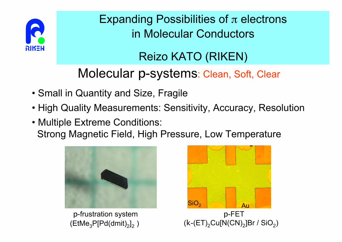
Expanding Possibilities of π electronsin Molecular Conductors
Reizo KATO (RIKEN)
• Small in Quantity and Size, Fragile
: Clean, Soft, Clear
• Multiple Extreme Conditions: Strong Magnetic Field, High Pressure, Low Temperature
Molecular p-systems
p-frustration system(EtMe3P[Pd(dmit)2]2 )
p-FET(k-(ET)2Cu[N(CN)2]Br / SiO2)
• High Quality Measurements: Sensitivity, Accuracy, Resolution
Au SiO2
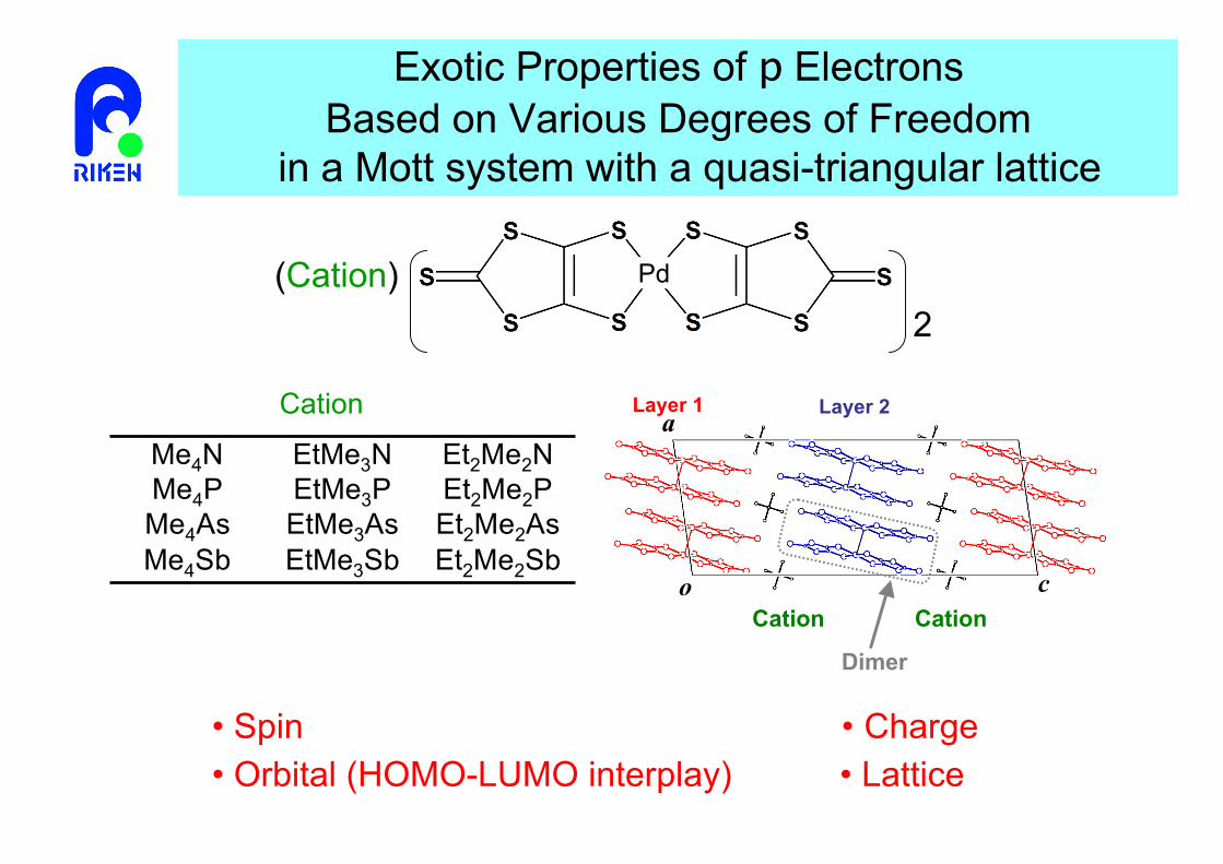
• Spin • Charge• Orbital (HOMO-LUMO interplay) • Lattice
Pd(Cation)2
Exotic Properties of p ElectronsBased on Various Degrees of Freedom
in a Mott system with a quasi-triangular lattice
Layer 1 Layer 2 a
o c Cation Cation
Dimer
Cation
Et2Me2SbEtMe3SbMe4SbEt2Me2AsEtMe3AsMe4AsEt2Me2PEtMe3PMe4PEt2Me2NEtMe3NMe4N
HOMO
LUMO
DE
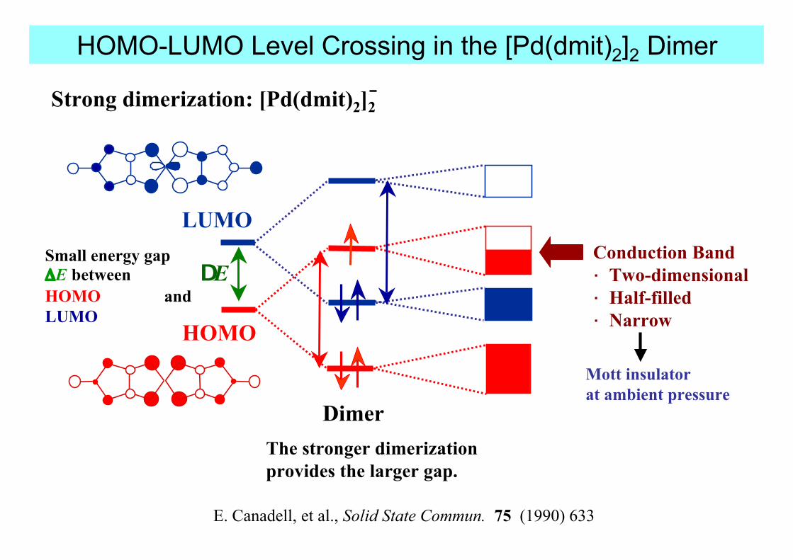
HOMO-LUMO Level Crossing in the [Pd(dmit)2]2 Dimer
Strong dimerization: [Pd(dmit)2]2
Small energy gapΔE betweenHOMO andLUMO
E. Canadell, et al., Solid State Commun. 75 (1990) 633
Conduction Band· Two-dimensional· Half-filled· Narrow
Mott insulatorat ambient pressure
DimerThe stronger dimerizationprovides the larger gap.
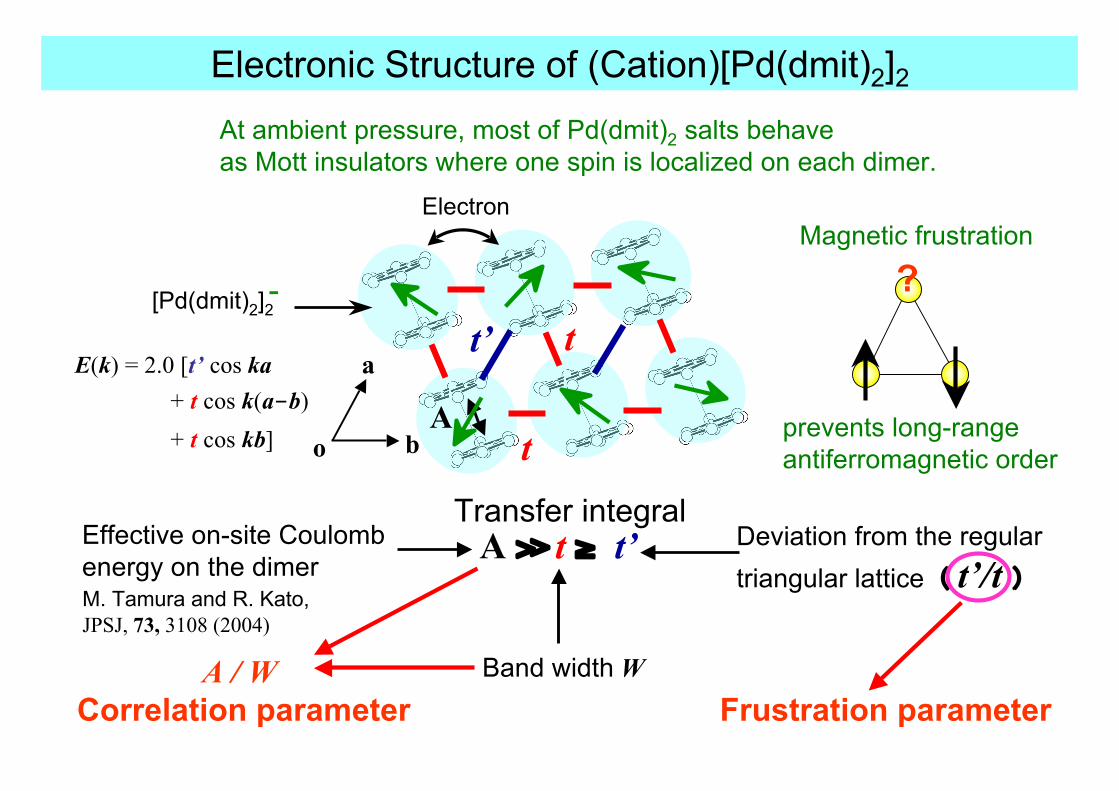
>A > t ≥ t’Transfer integral
Electrons move from dimer to dimer (Tight-binding approximation)
Band width W
Deviation from the regulartriangular lattice( t’/t )
Electron
A / W Correlation parameter
Effective on-site Coulombenergy on the dimerM. Tamura and R. Kato, JPSJ, 73, 3108 (2004)
Frustration parameter
At ambient pressure, most of Pd(dmit)2 salts behave as Mott insulators where one spin is localized on each dimer.
Electronic Structure of (Cation)[Pd(dmit)2]2
o b
at’ t
tA
Magnetic frustration
?
prevents long-rangeantiferromagnetic order
[Pd(dmit)2]2-
E(k) = 2.0 [t’ cos ka + t cos k(a-b) + t cos kb]
EtMe3Sb
Me4P
Me4As
EtMe3As
Me4SbEt2Me2AsEt2Me2P
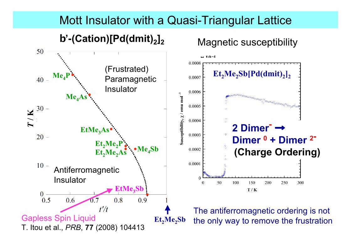
b’-(Cation)[Pd(dmit)2]2
The antiferromagnetic ordering is not the only way to remove the frustration Gapless Spin Liquid
T. Itou et al., PRB, 77 (2008) 104413
Antiferromagnetic Insulator
(Frustrated)ParamagneticInsulator
T / K
Magnetic susceptibility
EtMe3Sb
Me4P
100 200 3000
2
4
6
8× 10⁻⁴
T / Kc
/ cm
3 mol-1
0
TN
Et2Me2Sb[Pd(dmit)2]2
Mott Insulator with a Quasi-Triangular Lattice
2 Dimer- → Dimer 0 + Dimer 2- (Charge Ordering)
Et2Me2Sb
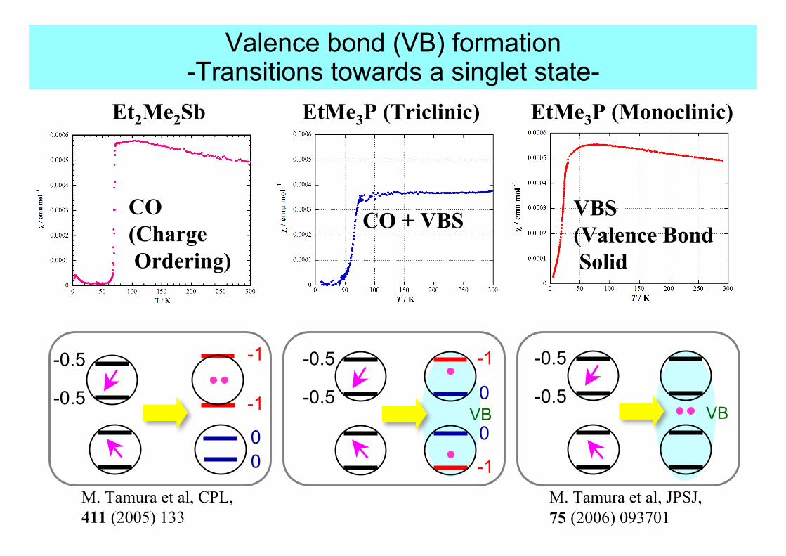
Valence bond (VB) formation-Transitions towards a singlet state-
CO + VBS
0
-1
0
-1
-0.5
-0.5VB
Et2Me2Sb EtMe3P (Triclinic) EtMe3P (Monoclinic)
CO(Charge Ordering)
-1
-1
00
-0.5
-0.5
M. Tamura et al, CPL, 411 (2005) 133
VBS(Valence Bond Solid
-0.5
-0.5VB
M. Tamura et al, JPSJ, 75 (2006) 093701
EtMe3Sb
Me4P
Me4As
EtMe3As
Me4SbEt2Me2AsEt2Me2P
Et2Me2Sb
b’-(Cation)[Pd(dmit)2]2
Antiferromagnetic Insulator
(Frustrated)ParamagneticInsulator
T / K
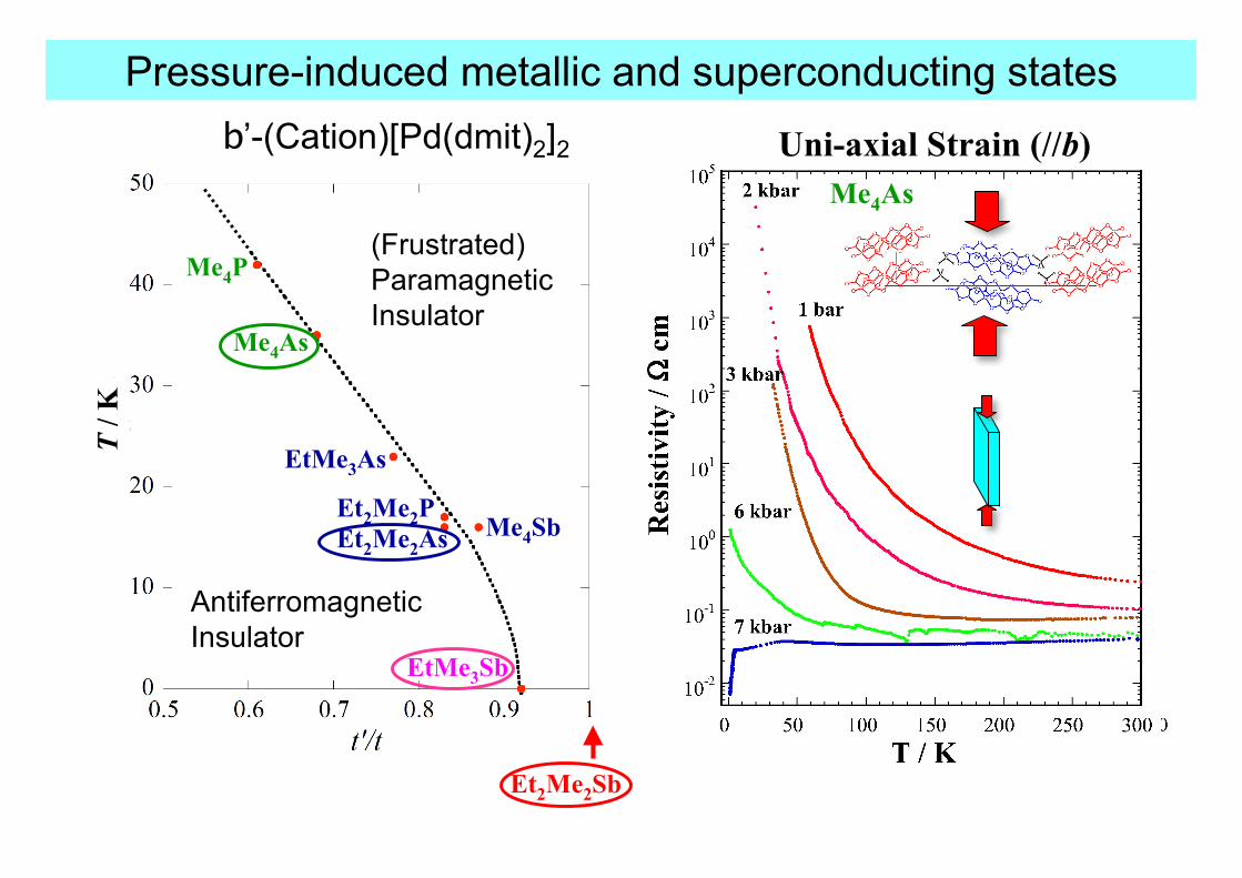
Pressure-induced metallic and superconducting states
Tc = 6 K
Et2Me2As
Uni-axial Strain (//b)Me4As
Photon energy (eV)
Ref
lect
ivity
0
-2
-1
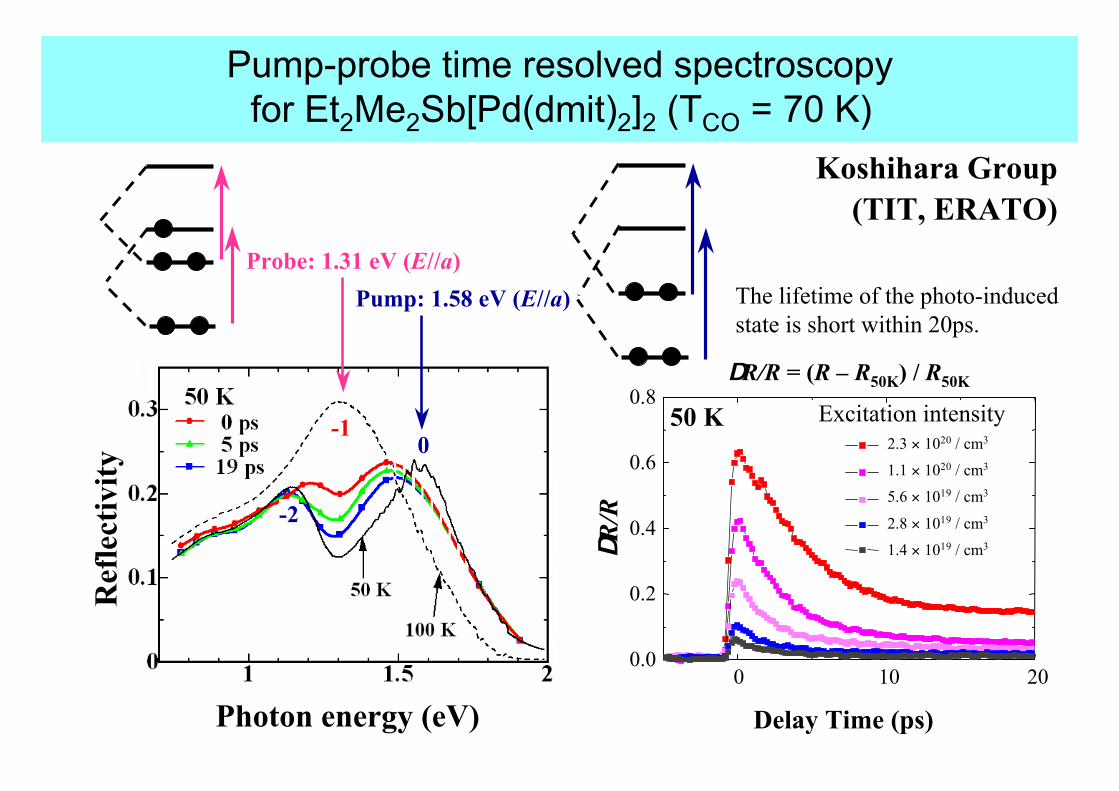
Pump: 1.58 eV (E//a)Probe: 1.31 eV (E//a)
0 10 200.0
0.2
0.4
0.6
0.8
DR/R
Delay Time (ps)
50 K
1.4 × 10¹⁹ / cm3
2.8 × 10¹⁹ / cm3
5.6 × 10¹⁹ / cm3
1.1 × 10²⁰ / cm3
2.3 × 10²⁰ / cm3
DR/R = (R – R50K) / R50K
Pump-probe time resolved spectroscopyfor Et2Me2Sb[Pd(dmit)2]2 (TCO = 70 K)
The lifetime of the photo-induced state is short within 20ps.
Koshihara Group(TIT, ERATO)
Excitation intensity
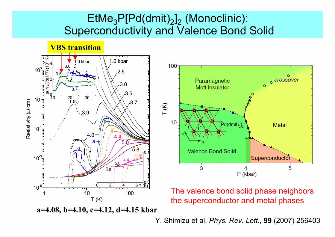
EtMe3P[Pd(dmit)2]2 (Monoclinic): Superconductivity and Valence Bond Solid
Y. Shimizu et al, Phys. Rev. Lett., 99 (2007) 256403
The valence bond solid phase neighbors the superconductor and metal phases
VBS transition
a=4.08, b=4.10, c=4.12, d=4.15 kbar
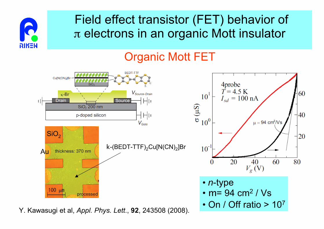
k-(BEDT-TTF)2Cu[N(CN)2]Br
• n-type• m = 94 cm2 / Vs• On / Off ratio > 107
Y. Kawasugi et al, Appl. Phys. Lett., 92, 243508 (2008).
Field effect transistor (FET) behavior ofπ electrons in an organic Mott insulator
Au
SiO2
Organic Mott FET
Expanding Possibilities of π electronsin Molecular Conductors
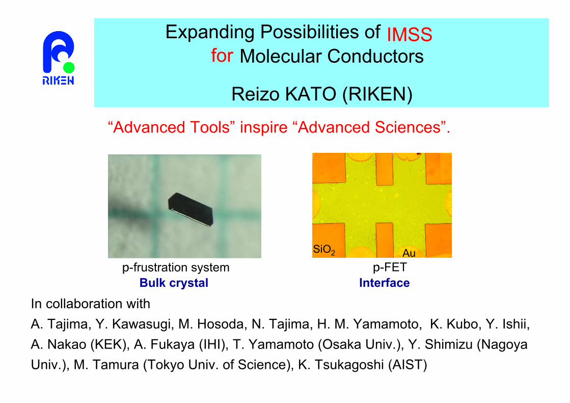
Reizo KATO (RIKEN)
“Advanced Tools” inspire “Advanced Sciences”.
IMSSfor
In collaboration withA. Tajima, Y. Kawasugi, M. Hosoda, N. Tajima, H. M. Yamamoto, K. Kubo, Y. Ishii,A. Nakao (KEK), A. Fukaya (IHI), T. Yamamoto (Osaka Univ.), Y. Shimizu (NagoyaUniv.), M. Tamura (Tokyo Univ. of Science), K. Tsukagoshi (AIST)
p-frustration systemBulk crystal
p-FETInterface
Au SiO2