LNA Design - dl.edatop.comdl.edatop.com/mte/ads/edatop.com_5-3LNA Design... · LNA Design Procedure...
33
LNA Design Single Stage AT41411 Study Case
Transcript of LNA Design - dl.edatop.comdl.edatop.com/mte/ads/edatop.com_5-3LNA Design... · LNA Design Procedure...
LNA Design
Single StageAT41411 Study Case
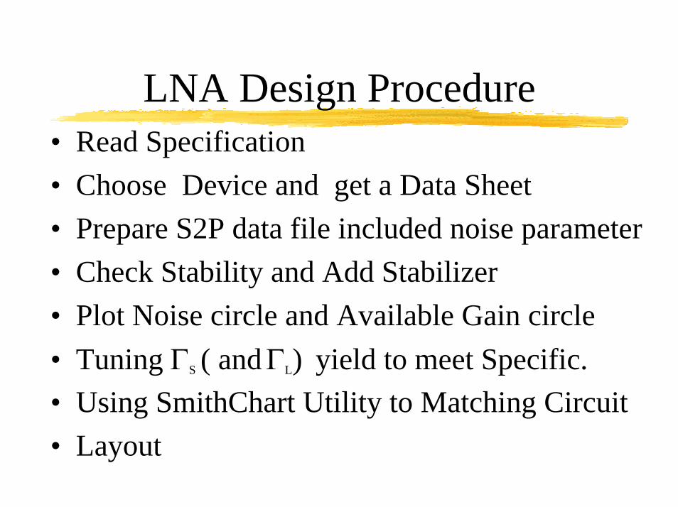
LNA Design Procedure• Read Specification• Choose Device and get a Data Sheet• Prepare S2P data file included noise parameter• Check Stability and Add Stabilizer• Plot Noise circle and Available Gain circle• Tuning ΓS ( andΓL) yield to meet Specific.• Using SmithChart Utility to Matching Circuit• Layout
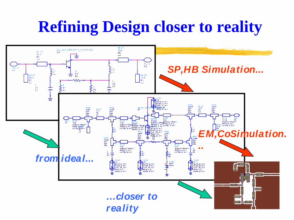
Refining Design closer to reality
from ideal...
…closer to reality
SP,HB Simulation...
EM,CoSimulation...
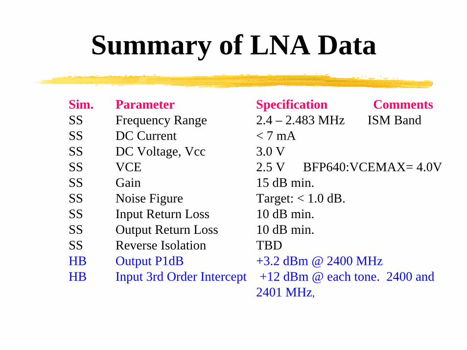
Summary of LNA Data
Sim. Parameter Specification CommentsSS Frequency Range 2.4 – 2.483 MHz ISM Band SS DC Current < 7 mASS DC Voltage, Vcc 3.0 V SS VCE 2.5 V BFP640:VCEMAX= 4.0VSS Gain 15 dB min. SS Noise Figure Target: < 1.0 dB. SS Input Return Loss 10 dB min. SS Output Return Loss 10 dB min. SS Reverse Isolation TBDHB Output P1dB +3.2 dBm @ 2400 MHz HB Input 3rd Order Intercept +12 dBm @ each tone. 2400 and
2401 MHz,
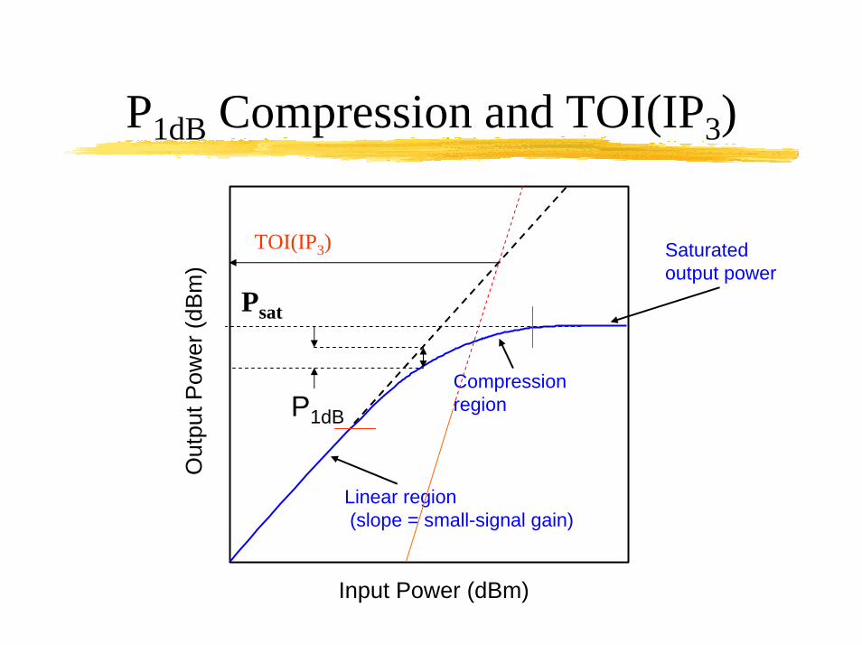
P1dB Compression and TOI(IP3)
Saturated output power
P1dB
Out
put P
ower
(dB
m)
Input Power (dBm)
Compression region
Linear region(slope = small-signal gain)
Psat
TOI(IP3)
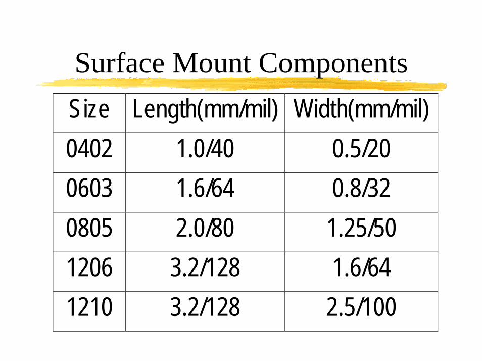
Surface Mount ComponentsSize Length(mm/mil) Width(mm/mil) 0402 1.0/40 0.5/20 0603 1.6/64 0.8/32 0805 2.0/80 1.25/50 1206 3.2/128 1.6/64 1210 3.2/128 2.5/100
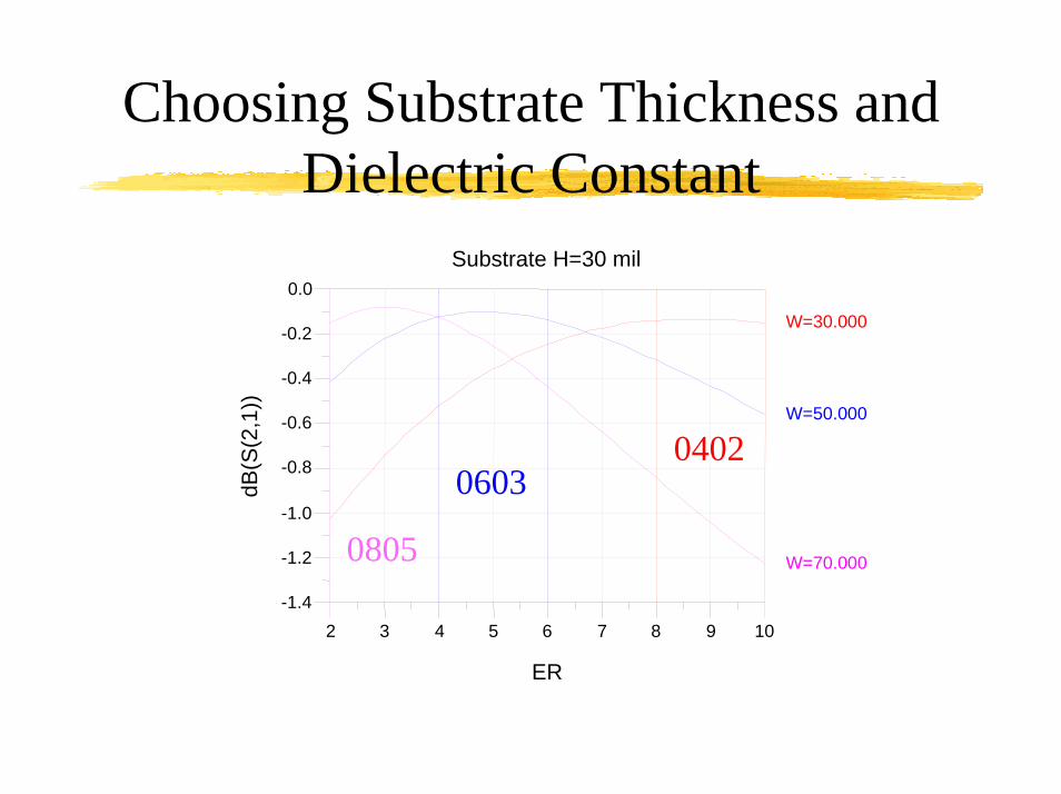
Choosing Substrate Thickness and Dielectric Constant
3 4 5 6 7 8 92 10
-1.2
-1.0
-0.8
-0.6
-0.4
-0.2
-1.4
0.0
W=30.000
W=50.000
W=70.000
ER
dB(S
(2,1
))Substrate H=30 mil
04020603
0805
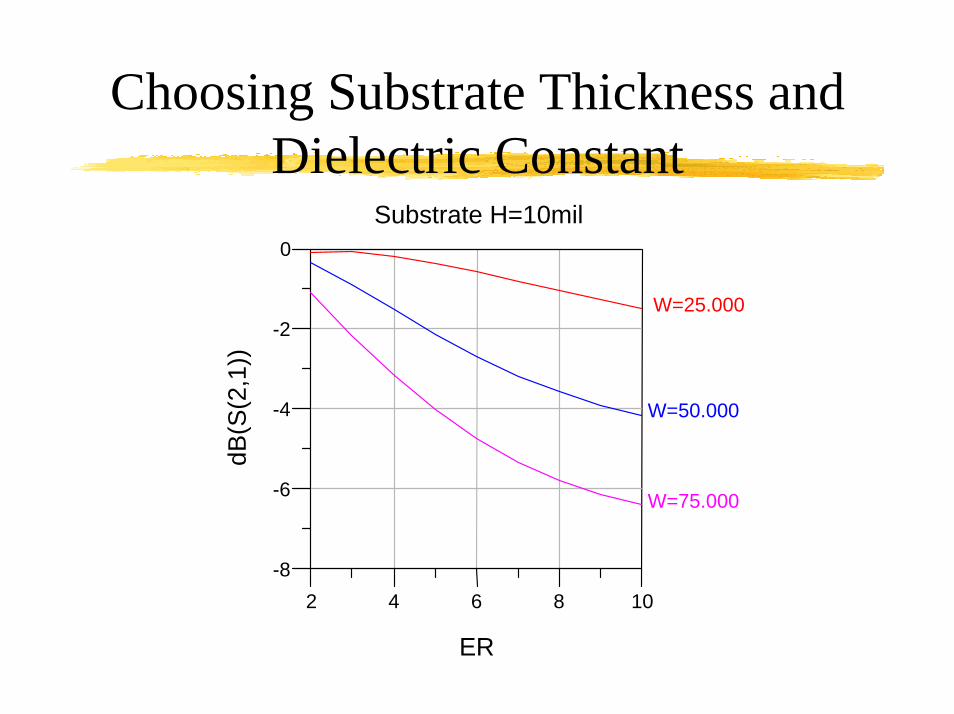
Choosing Substrate Thickness and Dielectric Constant
4 6 82 10
-6
-4
-2
-8
0
W=25.000
W=50.000
W=75.000
ER
dB(S
(2,1
))Substrate H=10mil
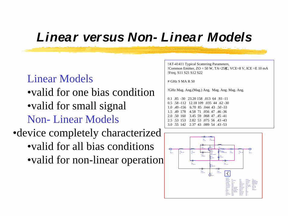
Linear versus Non- Linear Models
Linear Models•valid for one bias condition•valid for small signalNon- Linear Models
•device completely characterized•valid for all bias conditions•valid for non-linear operation
!AT-41411 Typical Scattering Parameters,!Common Emitter, ZO = 50 W, TA=25°C, VCE=8 V, ICE =E 10 mA!Freq. S11 S21 S12 S22
# GHz S MA R 50
!GHz Mag. Ang.(Mag.) Ang. Mag. Ang. Mag. Ang.
0.1 .85 -30 23.20 158 .013 64 .93 -110.5 .58 -112 12.18 109 .035 44 .62 -301.0 .49 -156 6.70 85 .044 43 .50 -331.5 .49 178 4.58 71 .056 47 .46 -362.0 .50 160 3.45 59 .068 47 .45 -412.5 .53 153 2.82 53 .075 56 .43 -433.0 .55 142 2.37 43 .089 54 .43 -53
BJT_ModelBJTM1
AllParams=Xti=3Xtb=-1.42Eg=1.078Trise=Tnom=24.85Approxqb=yesRbModel=MDSLateral=noFfe=
Nk=Ns=Iss=Rbnoi=Fb=Ab=Kb=Af=2Kf=7.291E-11Tr=0.2 nsecPtf=0Itf=0.4 AVtf=1.5 VTf=1.8 psecXtf=10
Fc=0.8Mjs=0.27Vjs=0.6 VCjs=93.4 fFXcjc=1Mjc=0.5Vjc=0.6 VCjc=67.43 fFMje=0.3Vje=0.8 VCje=227.6 fFImelt=Imax=Cco=Cex=
Dope=Rcm=Rcv=Rc=3.061 OhmRe=0.6 OhmRbm=2.707 OhmIrb=1.522 mARb=3.129 OhmVbo=Gbo=Cbo=Nc=1.8C4=Isc=400 fAKc=
Ke=Ikr=3.8 mAVar=2 VNr=1Br=55Ne=2C2=Ise=21 fAIkf=0.15 AVaf=1000 VNf=1.025Bf=450Is=0.22 fAPNP=noNPN=yes
BJT_NPNBJT1
Mode=nonlinearTrise=Temp=Region=Area=Model=BJTM1
RRBSR=1200 Ohm
PortENum=3
PortCNum=1
PortBNum=2
RRESR=300 Ohm
RRCSR=1200 Ohm
CCBEIC=180.4 fF
CCCEIC=112.6 fF
CCBEOC=102.5 fF
CCCEOC=131.2 fF
CCCSC=75 fF
CCBSC=79 fF
CCESC=180 fF
CCBCCC=55.9 fF
CCBECC=98.4 fF
LLEB
R=L=230.6 pH
LLCB
R=L=682.4 pH
LLBB
R=L=696.2 pH
LLEC
R=L=20 pH
LLCC
R=L=120 pH
LLBC
R=L=120 pH
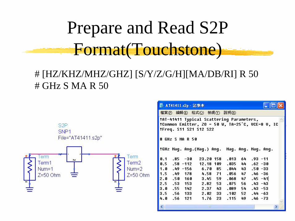
Prepare and Read S2P Format(Touchstone)
# [HZ/KHZ/MHZ/GHZ] [S/Y/Z/G/H][MA/DB/RI] R 50 # GHz S MA R 50
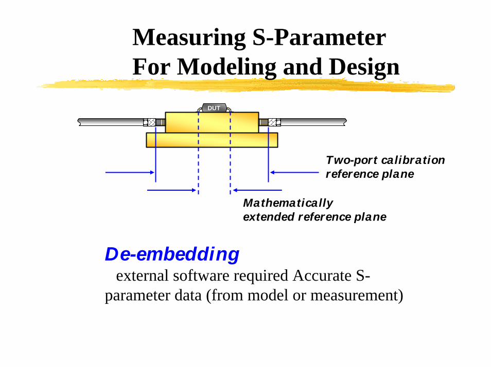
Measuring S-Parameter For Modeling and Design
Two-port calibration reference plane
DUT
Mathematically extended reference plane
De-embeddingexternal software required Accurate S-
parameter data (from model or measurement)
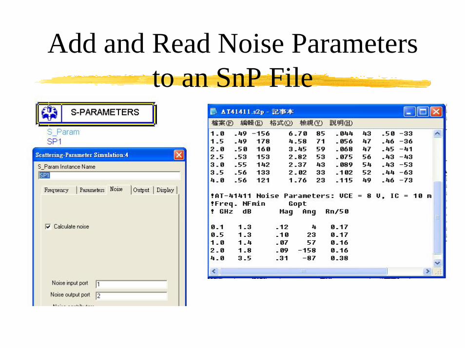
Add and Read Noise Parameters to an SnP File
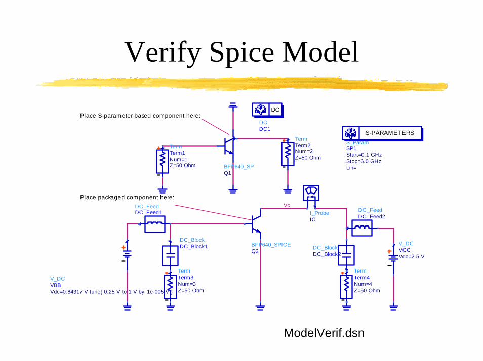
Verify Spice Model
Vc
Place packaged component here:
Place S-parameter-based component here:DCDC1
DC
I_ProbeIC
V_DCVBBVdc=0.84317 V tune{ 0.25 V to 1 V by 1e-005 V }
S_ParamSP1
Lin=Stop=6.0 GHzStart=0.1 GHz
S-PARAMETERS
V_DCVCCVdc=2.5 V
BFP640_SPICEQ2
TermTerm2
Z=50 OhmNum=2
BFP640_SPQ1
DC_BlockDC_Block2
DC_FeedDC_Feed2
TermTerm1
Z=50 OhmNum=1
TermTerm4
Z=50 OhmNum=4
DC_FeedDC_Feed1
DC_BlockDC_Block1
TermTerm3
Z=50 OhmNum=3
ModelVerif.dsn
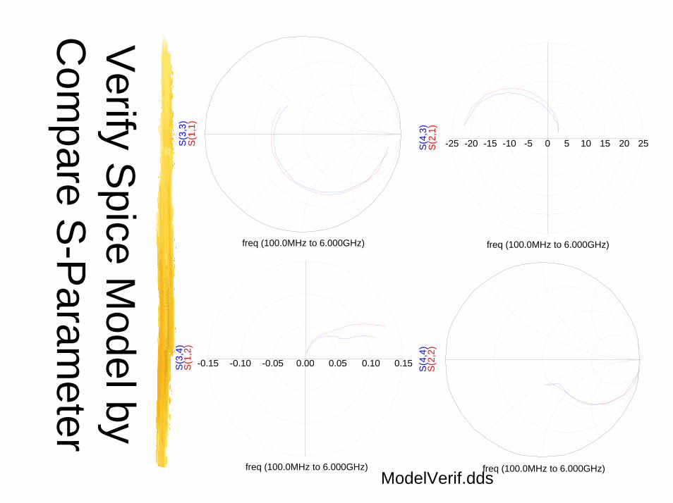
Verify S
pice Model by
Com
pare S-P
arameter
freq (100.0MHz to 6.000GHz)
S(1
,1)
S(3
,3)
freq (100.0MHz to 6.000GHz)
S(2
,2)
S(4
,4)
-0.10 -0.05 0.00 0.05 0.10-0.15 0.15
freq (100.0MHz to 6.000GHz)
S(1
,2)
S(3
,4)
-20 -15 -10 -5 0 5 10 15 20-25 25
freq (100.0MHz to 6.000GHz)
S(2
,1)
S(4
,3)
ModelVerif.dds
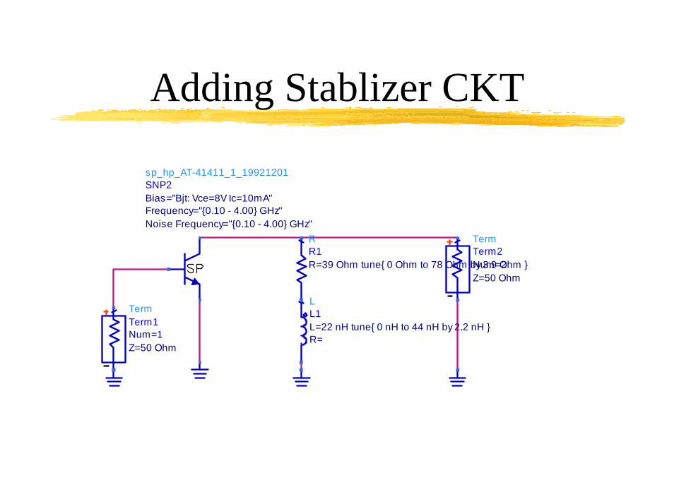
Adding Stablizer CKT
LL1
R=L=22 nH tune{ 0 nH to 44 nH by 2.2 nH }
RR1R=39 Ohm tune{ 0 Ohm to 78 Ohm by 3.9 Ohm }
TermTerm2
Z=50 OhmNum=2
TermTerm1
Z=50 OhmNum=1
sp_hp_AT-41411_1_19921201SNP2
Noise Frequency="{0.10 - 4.00} GHz"Frequency="{0.10 - 4.00} GHz"Bias="Bjt: Vce=8V Ic=10mA"
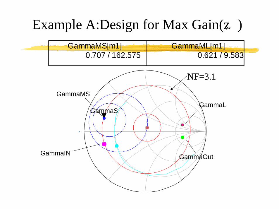
Example A:Design for Max Gain(一)GammaMS[m1]
0.707 / 162.575GammaML[m1]
0.621 / 9.583
NF=3.1
GammaS
GammaIN
GammaMS
GammaL
GammaOut
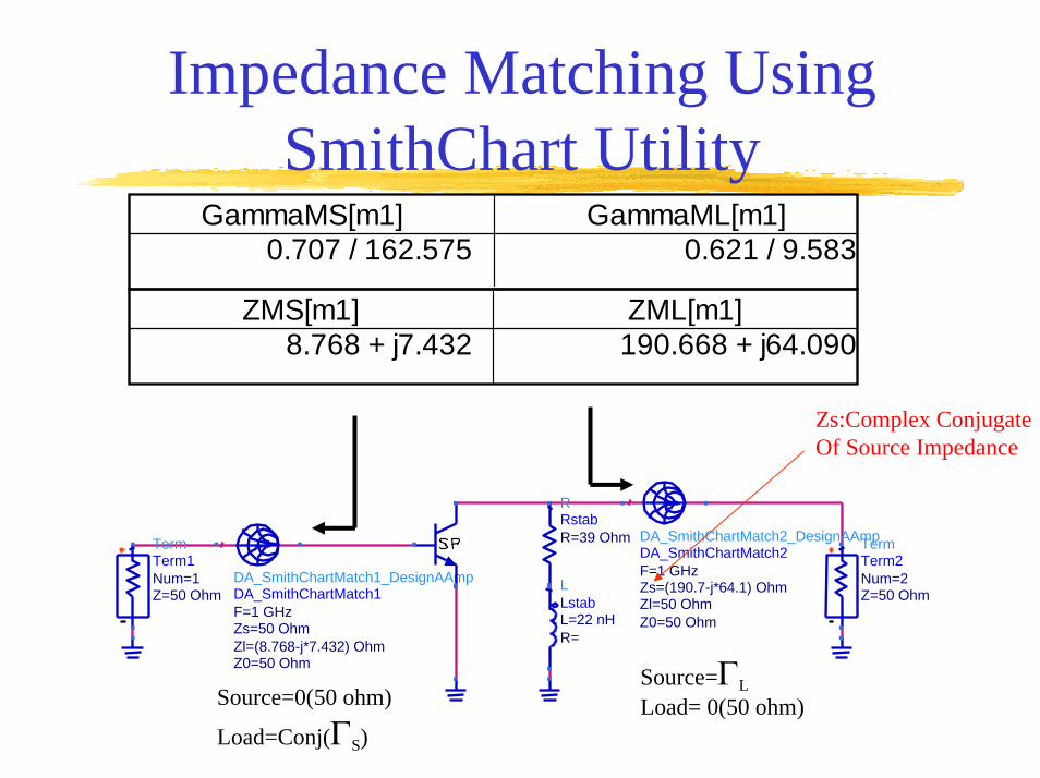
Impedance Matching Using SmithChart Utility
DA_SmithChartMatch1_DesignAAmpDA_SmithChartMatch1
Z0=50 OhmZl=(8.768-j*7.432) OhmZs=50 OhmF=1 GHz
DA_SmithChartMatch2_DesignAAmpDA_SmithChartMatch2
Z0=50 OhmZl=50 OhmZs=(190.7-j*64.1) OhmF=1 GHz
LLstab
R=L=22 nH
RRstabR=39 Ohm Term
Term2
Z=50 OhmNum=2
TermTerm1
Z=50 OhmNum=1
GammaMS[m1]0.707 / 162.575
GammaML[m1]0.621 / 9.583
ZMS[m1]8.768 + j7.432
ZML[m1]190.668 + j64.090
Source=0(50 ohm)
Load=Conj(ΓS)
Source=ΓLLoad= 0(50 ohm)
Zs:Complex ConjugateOf Source Impedance
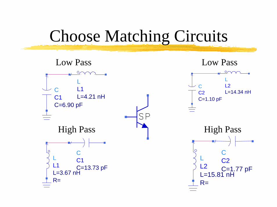
Choose Matching Circuits
CC1C=6.90 pF
LL1L=4.21 nH
Low Pass
LL2L=14.34 nH
CC2C=1.10 pF
Low Pass
CC1C=13.73 pF
LL1
R=L=3.67 nH
High Pass
CC2C=1.77 pF
LL2
R=L=15.81 nH
High Pass
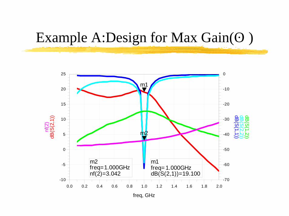
Example A:Design for Max Gain(二)
m1freq=dB(S(2,1))=19.100
1.000GHzm2freq=nf(2)=3.042
1.000GHz
0.2 0.4 0.6 0.8 1.0 1.2 1.4 1.6 1.80.0 2.0
-5
0
5
10
15
20
-10
25
-60
-50
-40
-30
-20
-10
-70
0
freq, GHz
dB(S
(2,1
))
m1
dB(S
(1,1))dB
(S(2,2))
dB(S
(1,2))nf
(2)
m2
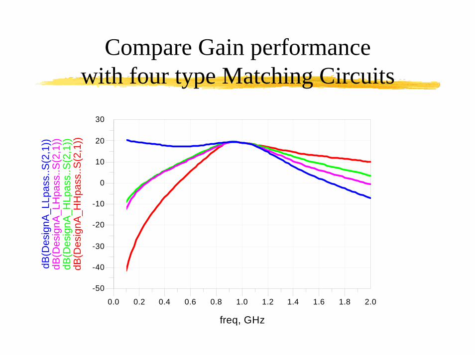
Compare Gain performancewith four type Matching Circuits
0.2 0.4 0.6 0.8 1.0 1.2 1.4 1.6 1.80.0 2.0
-40
-30
-20
-10
0
10
20
-50
30
freq, GHz
dB(D
esig
nA_H
Hpa
ss..S
(2,1
))dB
(Des
ignA
_HLp
ass.
.S(2
,1))
dB(D
esig
nA_L
Hpa
ss..S
(2,1
))dB
(Des
ignA
_LLp
ass.
.S(2
,1))
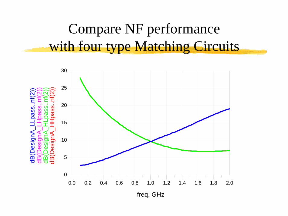
Compare NF performancewith four type Matching Circuits
0.2 0.4 0.6 0.8 1.0 1.2 1.4 1.6 1.80.0 2.0
5
10
15
20
25
0
30
freq, GHz
dB(D
esig
nA_H
Hpa
ss..n
f(2)
)dB
(Des
ignA
_HLp
ass.
.nf(
2))
dB(D
esig
nA_L
Hpa
ss..n
f(2)
)dB
(Des
ignA
_LLp
ass.
.nf(
2))
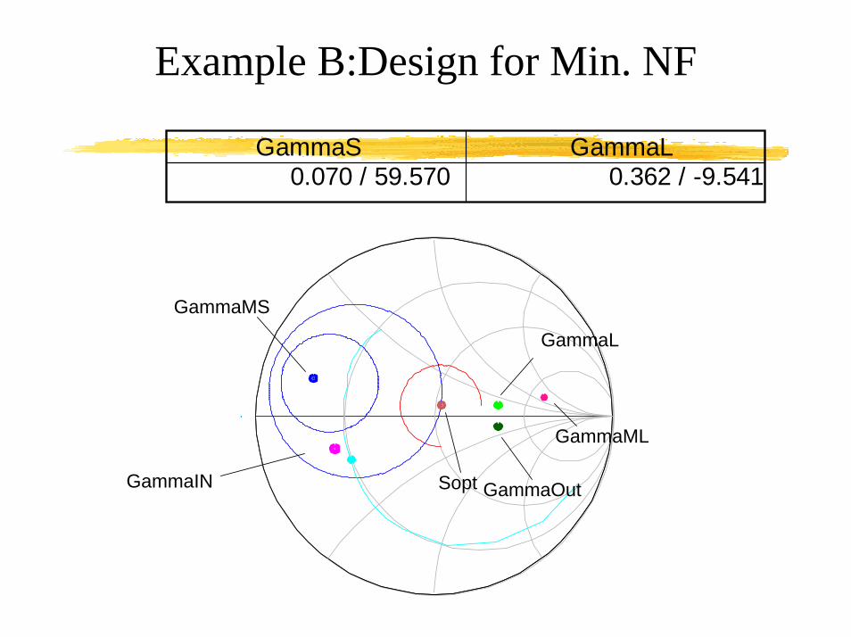
Example B:Design for Min. NF
GammaS0.070 / 59.570
GammaL0.362 / -9.541
GammaIN
GammaMS
GammaL
GammaOutSopt
GammaML
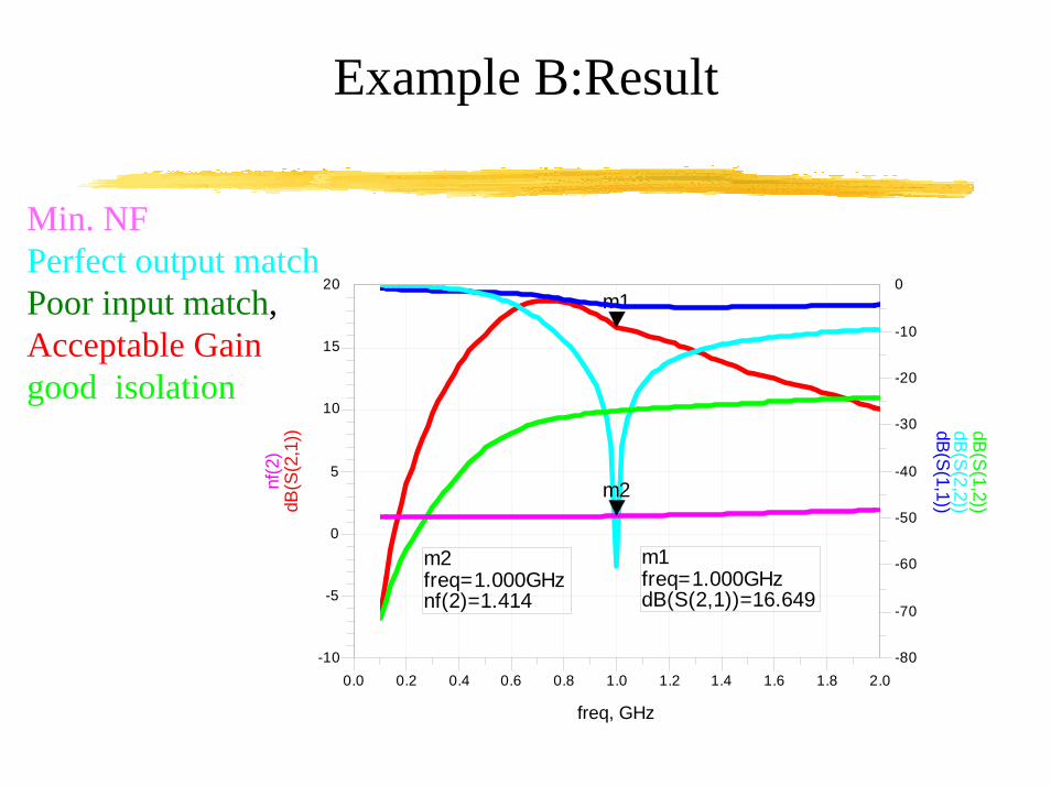
Example B:Result
Min. NFPerfect output matchPoor input match,Acceptable Gaingood isolation
m1freq=dB(S(2,1))=16.649
1.000GHzm2freq=nf(2)=1.414
1.000GHz
0.2 0.4 0.6 0.8 1.0 1.2 1.4 1.6 1.80.0 2.0
-5
0
5
10
15
-10
20
-70
-60
-50
-40
-30
-20
-10
-80
0
freq, GHz
dB(S
(2,1
))m1
dB(S
(1,1))dB
(S(2,2))
dB(S
(1,2))
nf(2
)
m2
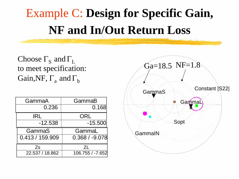
Example C: Design for Specific Gain, NF and In/Out Return Loss
Choose ΓS andΓL to meet specification:Gain,NF, Γa andΓb
GammaS
GammaIN
Sopt
GammaL
Constant |S22|
Ga=18.5 NF=1.8
GammaA0.236
GammaB0.168
IRL-12.538
ORL-15.500
GammaS0.413 / 159.909
GammaL0.368 / -9.078
Zs22.537 / 18.862
ZL106.755 / -7.652
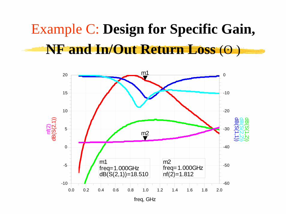
Example C: Design for Specific Gain, NF and In/Out Return Loss (二)
m1freq=dB(S(2,1))=18.510
1.000GHzm2freq=nf(2)=1.812
1.000GHz
0.2 0.4 0.6 0.8 1.0 1.2 1.4 1.6 1.80.0 2.0
-5
0
5
10
15
-10
20
-50
-40
-30
-20
-10
-60
0
freq, GHz
dB(S
(2,1
))
m1
dB(S
(1,1))dB
(S(2,2))
dB(S
(1,2))
nf(2
)
m2
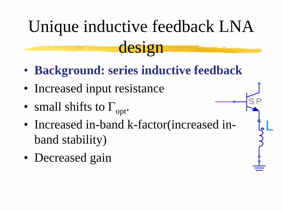
Unique inductive feedback LNA design
• Background: series inductive feedback• Increased input resistance• small shifts to Γopt.• Increased in-band k-factor(increased in-
band stability)• Decreased gain
L
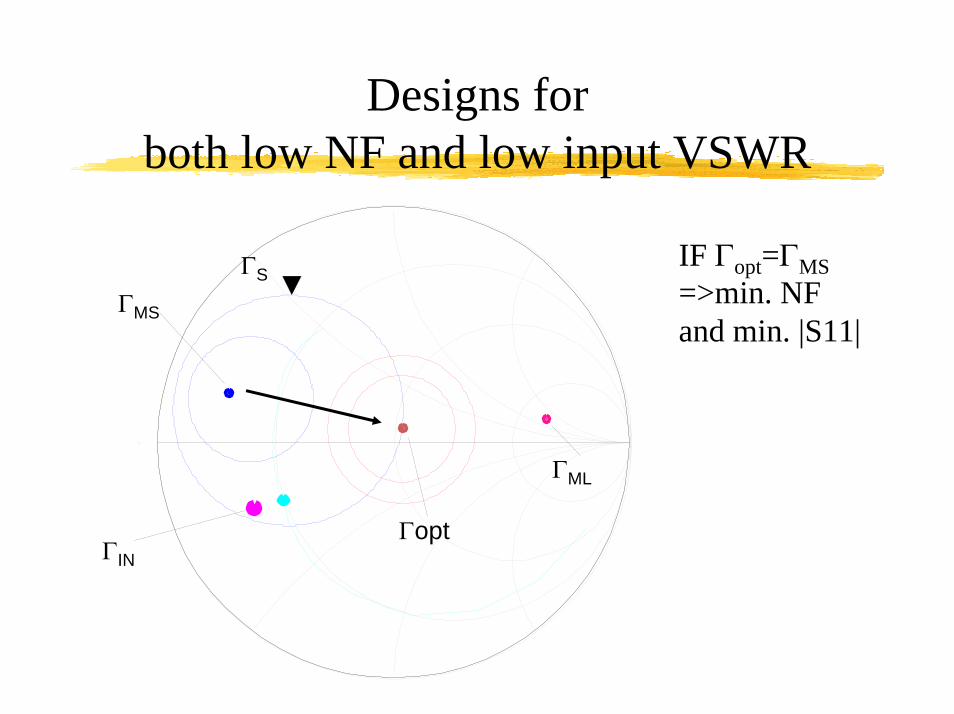
Designs for both low NF and low input VSWR
ΓS
Γopt
ΓML
ΓMS
ΓIN
IF Γopt=ΓMS=>min. NF and min. |S11|
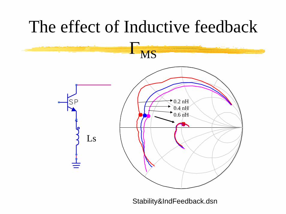
The effect of Inductive feedback ΓMS
0.2 nH0.4 nH0.6 nH
Ls
Stability&IndFeedback.dsn
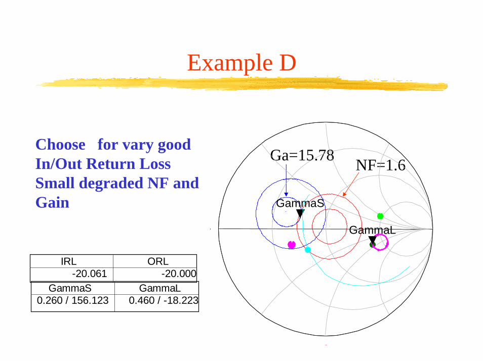
Example D
GammaS0.260 / 156.123
GammaL0.460 / -18.223
IRL-20.061
ORL-20.000
NF=1.6Ga=15.78
GammaS
GammaL
Choose for vary good In/Out Return Loss Small degraded NF and Gain
Example D:Result
m1freq=nf(2)=1.585
1.010GHzm2freq=dB(S(2,1))=15.739
1.000GHz
0.2 0.4 0.6 0.8 1.0 1.2 1.4 1.6 1.80.0 2.0
-30
-20
-10
0
10
-40
20
-50
-40
-30
-20
-10
-60
0
freq, GHz
dB
(S(2
,1))
m2
dB
(S(1
,1))
dB
(S(2
,2))
dB
(S(1
,2))
nf(
2)
m1
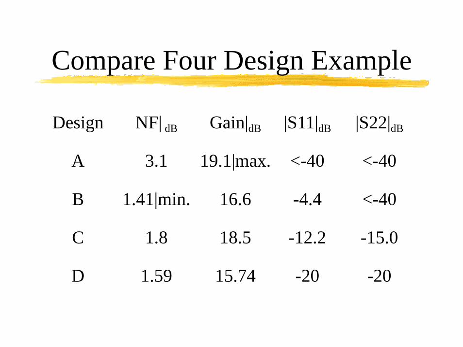
Compare Four Design Example
Design NF| dB Gain|dB |S11|dB |S22|dB
A 3.1 19.1|max. <-40 <-40
B 1.41|min. 16.6 -4.4 <-40
C 1.8 18.5 -12.2 -15.0
D 1.59 15.74 -20 -20

专注于微波、射频、天线设计人才的培养 易迪拓培训 网址:http://www.edatop.com
A D S 视 频 培 训 课 程 推 荐
ADS–Advanced Design System 是由原美国安捷伦科技(现更名为是德科技)推出的微波射频电路、
通信系统和 MMIC/RFIC 仿真设计软件,其功能强大、应用广泛,被国内高校、科研院所和大型科技
公司使用广为使用。掌握 ADS 无疑能提升相关设计领域工程师的技术实力、提高工作效率。
为了帮助工程技术人员更好、更快的学习掌握 ADS 的使用,易迪拓培训(www.edatop.com)特聘多
年 ADS 使用经验的资深专家精心制作推出了多套 ADS 视频培训课程,由浅入深、全面系统地讲授了
ADS 在微波射频电路设计、通信系统设计和电磁仿真设计方面的仿真设计和应用操作。其中,视频课
程多以设计实例边操作边讲解,工程实践强,且直观易学,能够帮助您在最短的时间内学会使用 ADS,
并把 ADS 真正应用到设计研发工作中去...
ADS 学习培训课程套装
该套装是易迪拓培训和微波 EDA 网联合推出的迄今为止国内最全面、最
权威的 ADS 培训教程,共包含 10 门 ADS 学习培训课程。课程是由具有
多年 ADS 使用经验的微波射频与通信系统设计领域资深专家讲解,并多
结合设计实例,由浅入深、详细而又全面地讲解了 ADS 在微波射频电路
设计、通信系统设计和电磁仿真设计方面的内容。能让您在最短的时间
内学会使用 ADS,迅速提升个人技术能力,把 ADS 真正应用到实际研发
工作中去,成为 ADS 设计专家...
课程网址: http://www.edatop.com/peixun/ads/13.html
更多 ADS 视频培训课程:
两周学会 ADS — 中文视频培训教程
最新版 ADS 的入门和进阶培训课程,适合 ADS2011 ~ ADS2014 以及更新版本 ADS 的学习。是
ADS 初学者的最佳课程,网址:http://www.edatop.com/peixun/ads/14.html
ADS 射频模拟电路设计详解 — 中文视频教程 本课程基于新版的 ADS 软件,由李明洋老师讲授,讲解了 ADS 在微波射频模拟电路设计中的具
体应用,视频课程,直观易学,网址:http://www.edatop.com/peixun/ads/15.html
ADS 高低阻抗线微带滤波器设计(ADS2014 版)— 中文视频教程
该门课程旨在帮助学员快速、全面、透彻地理解高低阻抗线微带滤波器的设计原理和设计步骤,
帮助学员学会并掌握使用 ADS 软件仿真分析和优化设计微带线滤波器的实际操作;课程网址:
http://www.edatop.com/peixun/filter/128.html
更多 ADS 培训课程,敬请浏览:http://www.edatop.com/peixun/ads

`
专注于微波、射频、天线设计人才的培养 易迪拓培训 网址:http://www.edatop.com
关于易迪拓培训:
易迪拓培训(www.edatop.com)由数名来自于研发第一线的资深工程师发起成立,一直致力和专注
于微波、射频、天线设计研发人才的培养;后于 2006 年整合合并微波 EDA 网(www.mweda.com),
现已发展成为国内最大的微波射频和天线设计人才培养基地,成功推出多套微波射频以及天线设计相
关培训课程和 ADS、HFSS 等专业软件使用培训课程,广受客户好评;并先后与人民邮电出版社、电
子工业出版社合作出版了多本专业图书,帮助数万名工程师提升了专业技术能力。客户遍布中兴通讯、
研通高频、埃威航电、国人通信等多家国内知名公司,以及台湾工业技术研究院、永业科技、全一电
子等多家台湾地区企业。
我们的课程优势:
※ 成立于 2004 年,10 多年丰富的行业经验
※ 一直专注于微波射频和天线设计工程师的培养,更了解该行业对人才的要求
※ 视频课程、既能达到现场培训的效果,又能免除您舟车劳顿的辛苦,学习工作两不误
※ 经验丰富的一线资深工程师讲授,结合实际工程案例,直观、实用、易学
联系我们:
※ 易迪拓培训官网:http://www.edatop.com
※ 微波 EDA 网:http://www.mweda.com
※ 官方淘宝店:http://shop36920890.taobao.com
专注于微波、射频、天线设计人才的培养
官方网址:http://www.edatop.com 易迪拓培训 淘宝网店:http://shop36920890.taobao.com