LH934A AC LED - · PDF fileHttp:// 7 /31 TABLE Rank CIE X CIE Y Rank CIE X CIE Y 3000K VB...
31
1 / 31 Http://www.samsungled.com Rev : 002 Features ㆍ Plastic Molded Lead Frame Type : 12.4㎜(L),11.4㎜(W), 4.38㎜(T) ㆍ SMD Type : 1 Heat Pad and 4 Electrical Pad ㆍ View Angle(△θ)* :136˚ ㆍ High Power / Brightness Chip & Long Time Reliability Applications ㆍ Indoor & Outdoor lighting ㆍ Direct AC power source plug-in (100~120Vac, 220~240Vac) SAMSUNG ELECTRONICS 95, Samsung2-Ro, Giheung-Gu, Yongin-City, Gyeonggi-Do 446-711, KOREA Copyright © 2009-2011 SAMSUNG ELECTRONICS Co.,Ltd. All rights reserved. The information in this document is subject to change without notice. SAMSUNG, is a registered trademark of SAMSUNG ELECTRONICS. Product Family Data Sheet LH934A - AC LED ISSUE NO : Introduction
Transcript of LH934A AC LED - · PDF fileHttp:// 7 /31 TABLE Rank CIE X CIE Y Rank CIE X CIE Y 3000K VB...
1 / 31Http://www.samsungled.com
Rev : 002
Featuresㆍ Plastic Molded Lead Frame Type :
12.4(L),11.4(W), 4.38(T)
ㆍ SMD Type : 1 Heat Pad and 4 Electrical Pad
ㆍ View Angle(θ)* :136˚ㆍ High Power / Brightness Chip & Long Time Reliability
Applicationsㆍ Indoor & Outdoor lighting
ㆍ Direct AC power source plug-in (100~120Vac, 220~240Vac)
SAMSUNG ELECTRONICS95, Samsung2-Ro, Giheung-Gu,
Yongin-City, Gyeonggi-Do 446-711, KOREA
Copyright © 2009-2011 SAMSUNG ELECTRONICS Co.,Ltd. All rights reserved. The information in this document is subject to
change without notice. SAMSUNG, is a registered trademark of SAMSUNG ELECTRONICS.
Product Family Data Sheet
LH934A - AC LED
ISSUE NO :
Introduction
2 / 31Http://www.samsungled.com
Contents
1. Product Outline ------------ 3
2. Absolute Maximum Rating ------------ 3
3. Electro-optical Characteristics ------------ 4
4. Color Binning ------------ 5
5. Chromaticity region & Coordinates ------------ 6
6. Luminous Flux ------------ 10
7. Vf Binning ------------ 11
8. Resistor Table ------------ 12
9. Typical Characteristic Graphs ------------ 13
10. Outline Drawing and Pad Configuration ------------ 17
11. Solder Conditions ------------ 18
12. Reliability Test Items & Conditions ------------ 19
13. Circuit Design - Package and PCB ------------ 20
14. Taping Dimension ------------ 21
15. Label Structure ------------ 22
16. Reel Packing Structure ------------ 23
17. Aluminum Packing Bag ------------ 25
18. Precaution For Use ------------ 26
19. Hazard Substance Analysis ------------ 28
Revision History ------------ 31
3 / 31Http://www.samsungled.com
1. Product Outline1) Features
ㆍ Plastic Molded Lead Frame Type : 12.4(L), 11.4(W), 4.38(T)ㆍ SMD Type : 1 Heat Pad and 4 Electrical Padㆍ Beam View Angle(θ)* :136˚ㆍ High Power / Brightness Chip & Long Time Reliability
2) Applicationsㆍ Indoor & Outdoor lightingㆍ Direct AC power source plug-in (100~120Vac, 220~240Vac)
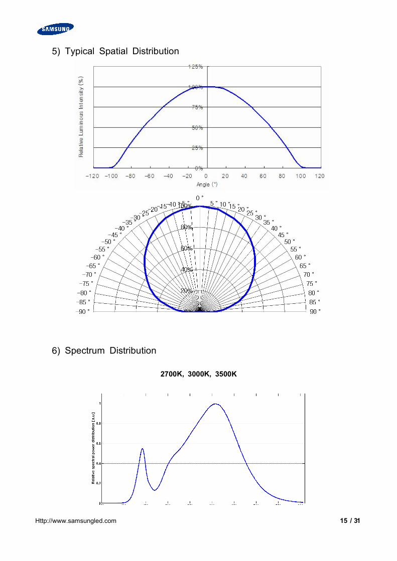
※ View Angle describes the spatial intensity distribution and is the difference between the anglescorresponding to 50% of the maximum intensity. (Full Width Half Maximum)
2. Absolute Maximum RatingParameter Value Unit
RMS current* 29**(240Vac) / 58**(120Vac) mA
Power Dissipation*** 4.5 W
LED Junction Temperature (TJ) 125
Operating Temperature Range (TOPR) -40 ∼ 85
Storage Temperature (TSTG) -40 ∼ 120
ESD Sensitivity ± 3,000V HBM -
*RMS (Root mean square) current indicates AC operation at 50~60Hz** Maximum current that can be fed into LEDs depends on their configuration. Refer to p.12 and p.20*** Average power dissipation only by the LED in AC operation. Power dissipation by any ballast
component that is connected to the LED is not included.
4 / 31Http://www.samsungled.com
3. Electro-optical Characteristics (Ta = 25 )
CCT [K] MinimumCRI
Luminous flux [ lm ]IF=22mA(rms) @ 220~240Vac*IF=44mA(rms) @ 100~120Vac**
IF=29mA(rms) @ 220~240VacIF=58mA(rms) @ 100~120Vac
Min. Typ. Typ.
2700
80
220 280 355
3000 240 290 365
3500 240 290 365
4000 260 300 375
500070
280 360 460
6500 250 330 460Power Dissipation*** 3.3W 4.5WOperating Frequency 50/60 Hz
*Max 29mA (RMS) current is allowed by 220~240Vac configuration. Refer to [ Resistor Table ] on p.12.**Max 58mA (RMS) current is allowed by 100~120Vac configuration. Refer to [ Resistor Table ] on p.12.***Average power dissipation only by the LED in AC operation. Power dissipation by any ballastcomponent that is connected to the LED is not included.
Notes :1) SAMSUNG ELECTRONICS maintains a tolerance of ±3.0 on CRI measurements.2) SAMSUNG ELECTRONICS maintains a tolerance of ±7% on flux measurements.
5 / 31Http://www.samsungled.com
4. Color Binning (Ta = 25 )
NominalCCT
Product Code Color Rank Chromaticity Bins
2700K
SPHWHTHAD605S0W0U4W0
(Whole Bin)WB,WC,WD,WE,WF,WG,WH
SPHWHTHAD605S0WUU4WU
(Half Bin)WB,WC,WD
SPHWHTHAD605S0WPU4WP
(M Sub Bin)WB
3000K
SPHWHTHAD605S0VOVZV0
(Whole Bin)VB,VC,VD,VE,VF,VG,VH
SPHWHTHAD605S0VUVZVU
(Half Bin)VB,VC,VD
SPHWHTHAD605S0VPVZVP
(M Sub Bin)VB
3500K
SPHWHTHAD605S0UOVZU0
(Whole Bin)UB,UC,UD,UE,UF,UG,UH
SPHWHTHAD605S0UUVZUU
(Half Bin)UB,UC,UD
SPHWHTHAD605S0UPVZUP
(M Sub Bin)UB
4000K
SPHWHTHAD605S0TOWZT0
(Whole Bin)TB,TC,TD,TE,TF,TG,TH
SPHWHTHAD605S0TUWZTU
(Half Bin)TB,TC,TD
SPHWHTHAD605S0TPWZTP
(M Sub Bin)TB
5000KSPHWHTHAD603S0R0MZ
R0(Whole Bin)
R1,R2,R3,R4,R5,R6,R7,R8
SPHWHTHAD603S0RTMZRT
(M Sub Bin)R1,R2,R3,R4
6500KSPHWHTHAD603S0P0LZ
P0(Whole Bin)
P1,P2,P3,P4,P5,P6,P7,P8
SPHWHTHAD603S0PTMZPT
(M Sub Bin)P1,P2,P3,P4
6 / 31Http://www.samsungled.com
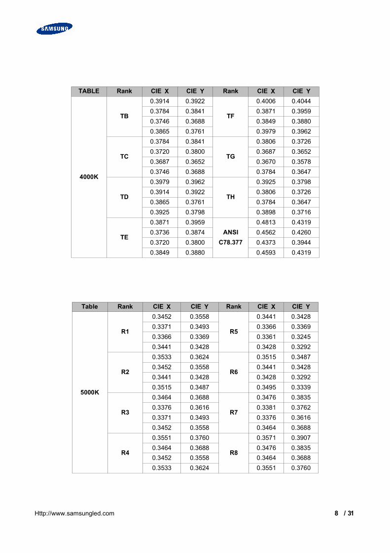
5. Chromaticity region & Coordinates (Ta = 25 )< CIE 1931 Chromaticity diagram >
TABLE Rank CIE X CIE Y Rank CIE X CIE Y
2700K
WB
0.4697 0.4211
WF
0.4813 0.43190.4576 0.4183 0.4688 0.42900.4477 0.3998 0.4636 0.41960.4591 0.4024 0.4758 0.4225
WC
0.4576 0.4183
WG
0.4534 0.40120.4515 0.4168 0.4420 0.39850.4420 0.3985 0.4373 0.38930.4477 0.3998 0.4483 0.3919
WD
0.4758 0.4225
WH
0.4648 0.40380.4697 0.4211 0.4534 0.40120.4591 0.4024 0.4483 0.39190.4648 0.4038 0.4593 0.3944
WE
0.4688 0.4290
ANSI
0.4813 0.43190.4562 0.4260 0.4562 0.42600.4515 0.4168 0.4373 0.39440.4636 0.4196 0.4593 0.4319
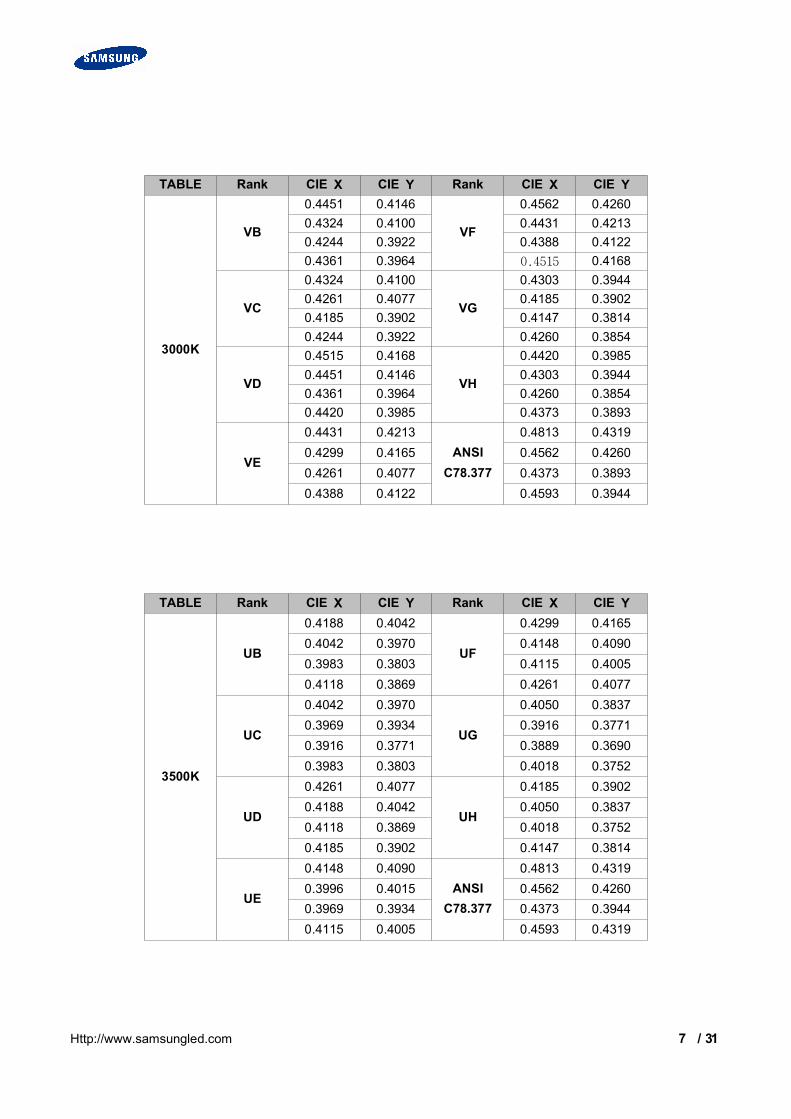
7 / 31Http://www.samsungled.com
TABLE Rank CIE X CIE Y Rank CIE X CIE Y
3000K
VB
0.4451 0.4146
VF
0.4562 0.42600.4324 0.4100 0.4431 0.42130.4244 0.3922 0.4388 0.41220.4361 0.3964 0.4515 0.4168
VC
0.4324 0.4100
VG
0.4303 0.39440.4261 0.4077 0.4185 0.39020.4185 0.3902 0.4147 0.38140.4244 0.3922 0.4260 0.3854
VD
0.4515 0.4168
VH
0.4420 0.39850.4451 0.4146 0.4303 0.39440.4361 0.3964 0.4260 0.38540.4420 0.3985 0.4373 0.3893
VE
0.4431 0.4213ANSI
C78.377
0.4813 0.43190.4299 0.4165 0.4562 0.42600.4261 0.4077 0.4373 0.38930.4388 0.4122 0.4593 0.3944
TABLE Rank CIE X CIE Y Rank CIE X CIE Y
3500K
UB
0.4188 0.4042
UF
0.4299 0.41650.4042 0.3970 0.4148 0.40900.3983 0.3803 0.4115 0.40050.4118 0.3869 0.4261 0.4077
UC
0.4042 0.3970
UG
0.4050 0.38370.3969 0.3934 0.3916 0.37710.3916 0.3771 0.3889 0.36900.3983 0.3803 0.4018 0.3752
UD
0.4261 0.4077
UH
0.4185 0.39020.4188 0.4042 0.4050 0.38370.4118 0.3869 0.4018 0.37520.4185 0.3902 0.4147 0.3814
UE
0.4148 0.4090ANSI
C78.377
0.4813 0.43190.3996 0.4015 0.4562 0.42600.3969 0.3934 0.4373 0.39440.4115 0.4005 0.4593 0.4319
8 / 31Http://www.samsungled.com
TABLE Rank CIE X CIE Y Rank CIE X CIE Y
4000K
TB
0.3914 0.3922
TF
0.4006 0.40440.3784 0.3841 0.3871 0.39590.3746 0.3688 0.3849 0.38800.3865 0.3761 0.3979 0.3962
TC
0.3784 0.3841
TG
0.3806 0.37260.3720 0.3800 0.3687 0.36520.3687 0.3652 0.3670 0.35780.3746 0.3688 0.3784 0.3647
TD
0.3979 0.3962
TH
0.3925 0.37980.3914 0.3922 0.3806 0.37260.3865 0.3761 0.3784 0.36470.3925 0.3798 0.3898 0.3716
TE
0.3871 0.3959ANSI
C78.377
0.4813 0.43190.3736 0.3874 0.4562 0.42600.3720 0.3800 0.4373 0.39440.3849 0.3880 0.4593 0.4319
Table Rank CIE X CIE Y Rank CIE X CIE Y
5000K
R1
0.3452 0.3558
R5
0.3441 0.34280.3371 0.3493 0.3366 0.33690.3366 0.3369 0.3361 0.32450.3441 0.3428 0.3428 0.3292
R2
0.3533 0.3624
R6
0.3515 0.34870.3452 0.3558 0.3441 0.34280.3441 0.3428 0.3428 0.32920.3515 0.3487 0.3495 0.3339
R3
0.3464 0.3688
R7
0.3476 0.38350.3376 0.3616 0.3381 0.37620.3371 0.3493 0.3376 0.36160.3452 0.3558 0.3464 0.3688
R4
0.3551 0.3760
R8
0.3571 0.39070.3464 0.3688 0.3476 0.38350.3452 0.3558 0.3464 0.36880.3533 0.3624 0.3551 0.3760
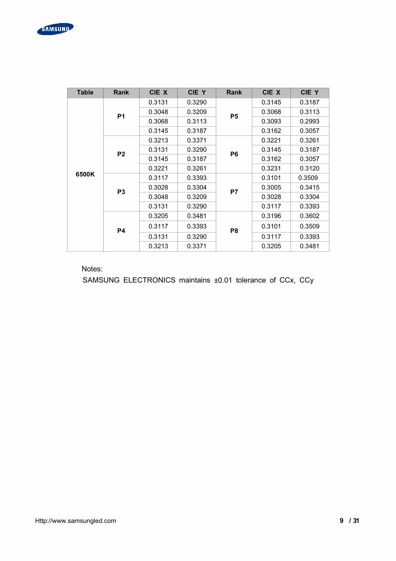
9 / 31Http://www.samsungled.com
Table Rank CIE X CIE Y Rank CIE X CIE Y
6500K
P1
0.3131 0.3290
P5
0.3145 0.31870.3048 0.3209 0.3068 0.31130.3068 0.3113 0.3093 0.29930.3145 0.3187 0.3162 0.3057
P2
0.3213 0.3371
P6
0.3221 0.32610.3131 0.3290 0.3145 0.31870.3145 0.3187 0.3162 0.30570.3221 0.3261 0.3231 0.3120
P3
0.3117 0.3393
P7
0.3101 0.35090.3028 0.3304 0.3005 0.34150.3048 0.3209 0.3028 0.33040.3131 0.3290 0.3117 0.3393
P4
0.3205 0.3481
P8
0.3196 0.36020.3117 0.3393 0.3101 0.35090.3131 0.3290 0.3117 0.33930.3213 0.3371 0.3205 0.3481
Notes:SAMSUNG ELECTRONICS maintains ±0.01 tolerance of CCx, CCy
10 / 31Http://www.samsungled.com
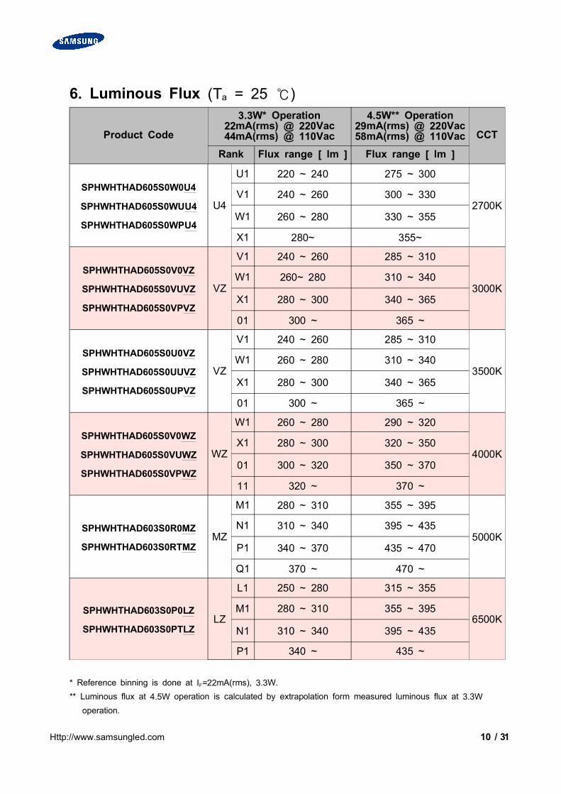
6. Luminous Flux (Ta = 25 )
Product Code
3.3W* Operation22mA(rms) @ 220Vac44mA(rms) @ 110Vac
4.5W** Operation29mA(rms) @ 220Vac58mA(rms) @ 110Vac CCT
Rank Flux range [ lm ] Flux range [ lm ]
SPHWHTHAD605S0W0U4
SPHWHTHAD605S0WUU4
SPHWHTHAD605S0WPU4
U4
U1 220 ~ 240 275 ~ 300
2700KV1 240 ~ 260 300 ~ 330
W1 260 ~ 280 330 ~ 355
X1 280~ 355~
SPHWHTHAD605S0V0VZ
SPHWHTHAD605S0VUVZ
SPHWHTHAD605S0VPVZ
VZ
V1 240 ~ 260 285 ~ 310
3000KW1 260~ 280 310 ~ 340
X1 280 ~ 300 340 ~ 365
01 300 ~ 365 ~
SPHWHTHAD605S0U0VZ
SPHWHTHAD605S0UUVZ
SPHWHTHAD605S0UPVZ
VZ
V1 240 ~ 260 285 ~ 310
3500KW1 260 ~ 280 310 ~ 340
X1 280 ~ 300 340 ~ 365
01 300 ~ 365 ~
SPHWHTHAD605S0V0WZ
SPHWHTHAD605S0VUWZ
SPHWHTHAD605S0VPWZ
WZ
W1 260 ~ 280 290 ~ 320
4000KX1 280 ~ 300 320 ~ 350
01 300 ~ 320 350 ~ 370
11 320 ~ 370 ~
SPHWHTHAD603S0R0MZ
SPHWHTHAD603S0RTMZMZ
M1 280 ~ 310 355 ~ 395
5000KN1 310 ~ 340 395 ~ 435
P1 340 ~ 370 435 ~ 470
Q1 370 ~ 470 ~
SPHWHTHAD603S0P0LZ
SPHWHTHAD603S0PTLZLZ
L1 250 ~ 280 315 ~ 355
6500KM1 280 ~ 310 355 ~ 395
N1 310 ~ 340 395 ~ 435
P1 340 ~ 435 ~
* Reference binning is done at IF=22mA(rms), 3.3W.** Luminous flux at 4.5W operation is calculated by extrapolation form measured luminous flux at 3.3W
operation.
11 / 31Http://www.samsungled.com
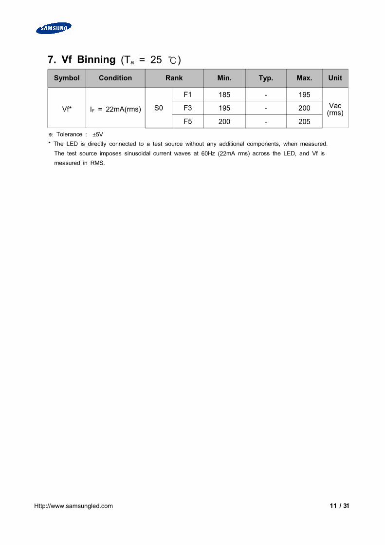
7. Vf Binning (Ta = 25 )Symbol Condition Rank Min. Typ. Max. Unit
Vf* IF = 22mA(rms) S0
F1 185 - 195Vac(rms)
F3 195 - 200
F5 200 - 205
※ Tolerance : ±5V* The LED is directly connected to a test source without any additional components, when measured.The test source imposes sinusoidal current waves at 60Hz (22mA rms) across the LED, and Vf ismeasured in RMS.
12 / 31Http://www.samsungled.com
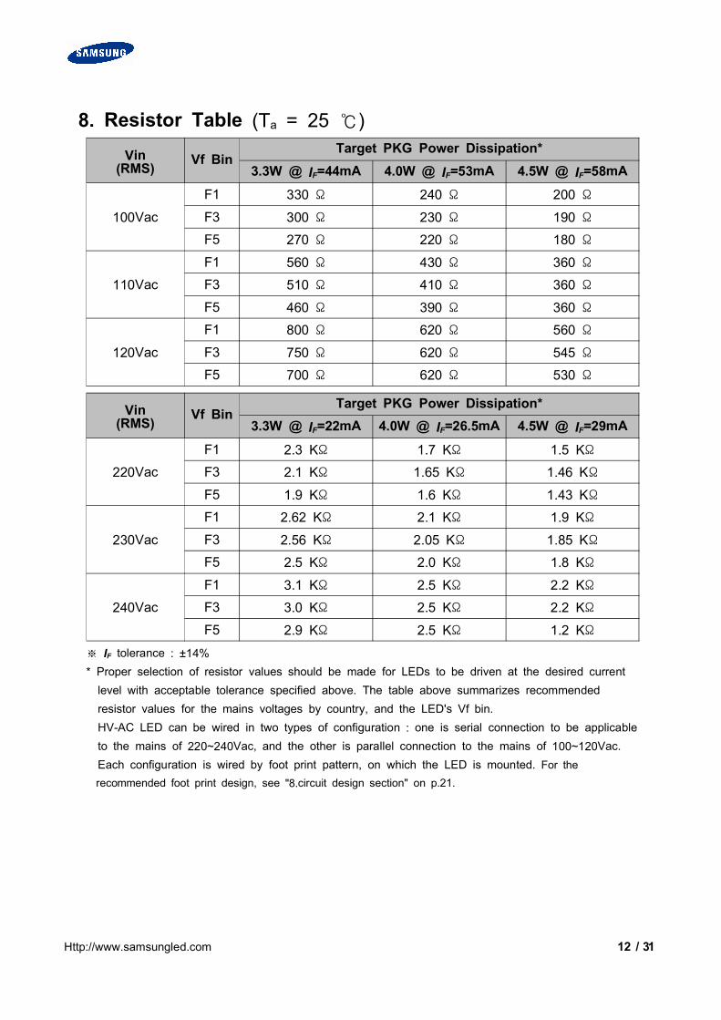
8. Resistor Table (Ta = 25 )
Vin(RMS) Vf Bin
Target PKG Power Dissipation*3.3W @ IF=44mA 4.0W @ IF=53mA 4.5W @ IF=58mA
100Vac
F1 330 Ω 240 Ω 200 Ω
F3 300 Ω 230 Ω 190 Ω
F5 270 Ω 220 Ω 180 Ω
110Vac
F1 560 Ω 430 Ω 360 Ω
F3 510 Ω 410 Ω 360 Ω
F5 460 Ω 390 Ω 360 Ω
120Vac
F1 800 Ω 620 Ω 560 Ω
F3 750 Ω 620 Ω 545 Ω
F5 700 Ω 620 Ω 530 Ω
Vin(RMS) Vf Bin
Target PKG Power Dissipation*3.3W @ IF=22mA 4.0W @ IF=26.5mA 4.5W @ IF=29mA
220Vac
F1 2.3 KΩ 1.7 KΩ 1.5 KΩ
F3 2.1 KΩ 1.65 KΩ 1.46 KΩ
F5 1.9 KΩ 1.6 KΩ 1.43 KΩ
230Vac
F1 2.62 KΩ 2.1 KΩ 1.9 KΩ
F3 2.56 KΩ 2.05 KΩ 1.85 KΩ
F5 2.5 KΩ 2.0 KΩ 1.8 KΩ
240Vac
F1 3.1 KΩ 2.5 KΩ 2.2 KΩ
F3 3.0 KΩ 2.5 KΩ 2.2 KΩ
F5 2.9 KΩ 2.5 KΩ 1.2 KΩ
※ IF tolerance : ±14%* Proper selection of resistor values should be made for LEDs to be driven at the desired currentlevel with acceptable tolerance specified above. The table above summarizes recommendedresistor values for the mains voltages by country, and the LED's Vf bin.HV-AC LED can be wired in two types of configuration : one is serial connection to be applicableto the mains of 220~240Vac, and the other is parallel connection to the mains of 100~120Vac.Each configuration is wired by foot print pattern, on which the LED is mounted. For therecommended foot print design, see "8.circuit design section" on p.21.
13 / 31Http://www.samsungled.com
9. Typical Characteristic Graphs1) AC voltage operating characteristic
Total Power Consumption = Power_LED + Power_ResistorPower_LED = Total Power - I2R
< Power consumption vs. Operating current >
0
1
2
3
4
5
6
7
0 10 20 30 40
Operating Current [mA rms]
Consum
ption P
ow
er
[W
]
.
Power_total
Power_LED
Power_Resistor
< LED Input Power vs. Generated Heat >
0.0
0.5
1.0
1.5
2.0
2.5
3.0
3.5
4.0
0 2 4 6
Input Power [W]
Genera
ted H
eat
[W
]
.
※ Total Thermal dissipation = LED + ResistorThermal dissipation of the LED is the vertical axis of the above graph.Thermal dissipation of the resistor is Current2 X Resistance.Proper resistor value and type must be selected depending on the operating condition.
BallastResistor
14 / 31Http://www.samsungled.com
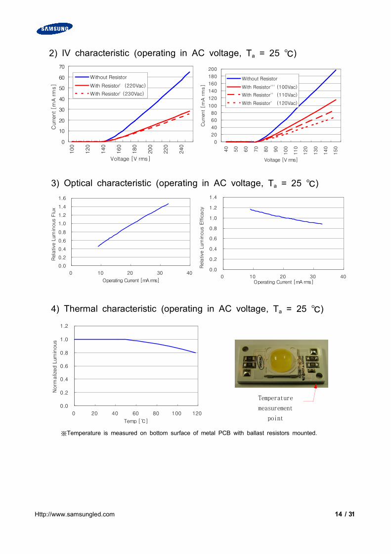
2) IV characteristic (operating in AC voltage, Ta = 25 )
0
10
20
30
40
50
60
70100
120
140
160
180
200
220
240
Voltage [V rms]
Current [m
A rm
s]
.
Without Resistor
With Resistor' (220Vac)
With Resistor' (230Vac)
0
20
40
60
80
100
120
140
160
180
200
40
50
60
70
80
90
100
110
120
130
140
150
Voltage [V rms]
Curr
ent
[m
A r
ms]
.
Without Resistor
With Resistor''' (100Vac)
With Resistor'' (110Vac)
With Resistor' (120Vac)
3) Optical characteristic (operating in AC voltage, Ta = 25 )
0.0
0.2
0.4
0.6
0.8
1.0
1.2
1.4
1.6
0 10 20 30 40
Operating Current [mA rms]
Rela
tive
Lum
inous F
lux
.
0.0
0.2
0.4
0.6
0.8
1.0
1.2
1.4
0 10 20 30 40Operating Current [mA rms]
Rela
tive
Lum
inous E
ffic
acy
.
4) Thermal characteristic (operating in AC voltage, Ta = 25 )
0.0
0.2
0.4
0.6
0.8
1.0
1.2
0 20 40 60 80 100 120
Temp []
Norm
aliz
ed L
um
inous .
※Temperature is measured on bottom surface of metal PCB with ballast resistors mounted.
Temperature
measurement
point
15 / 31Http://www.samsungled.com
5) Typical Spatial Distribution
6) Spectrum Distribution
2700K, 3000K, 3500K
16 / 31Http://www.samsungled.com
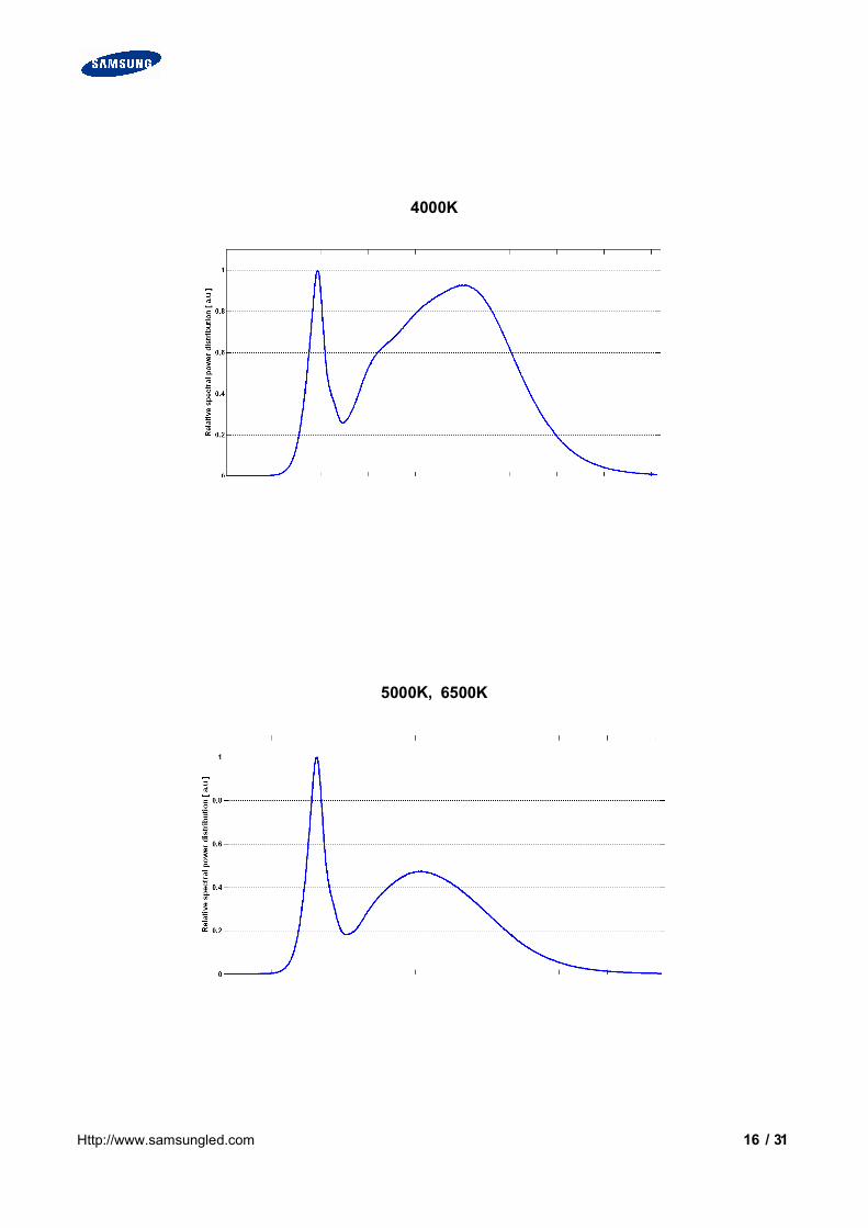
4000K
5000K, 6500K
17 / 31Http://www.samsungled.com
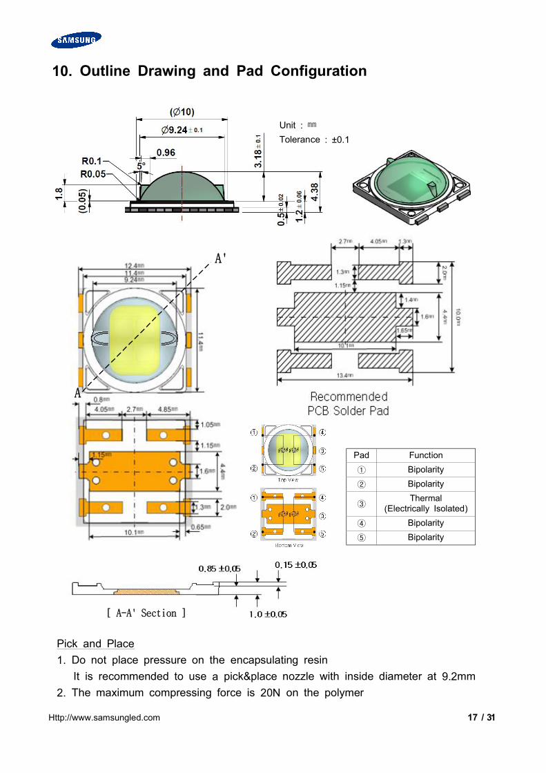
10. Outline Drawing and Pad Configuration
Unit :
Tolerance : ±0.1
Pad Function
① Bipolarity
② Bipolarity
③Thermal
(Electrically Isolated)
④ Bipolarity
⑤ Bipolarity
Pick and Place1. Do not place pressure on the encapsulating resin
It is recommended to use a pick&place nozzle with inside diameter at 9.2mm2. The maximum compressing force is 20N on the polymer
A'
A
[ A-A' Section ]
18 / 31Http://www.samsungled.com
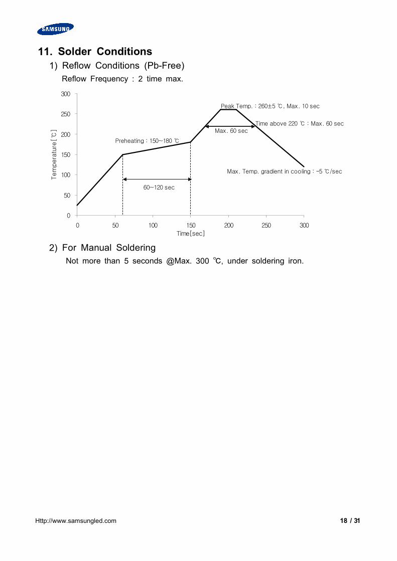
11. Solder Conditions1) Reflow Conditions (Pb-Free)
Reflow Frequency : 2 time max.
2) For Manual SolderingNot more than 5 seconds @Max. 300 , under soldering iron.
0
50
100
150
200
250
300
0 50 100 150 200 250 300
Time[sec]
Tem
pera
ture
[
] 0
Preheating : 150~180
Peak Temp. : 260±5 , Max. 10 sec
Max. 60 secTime above 220 : Max. 60 sec
Max. Temp. gradient in cooling : -5 /sec
60~120 sec
19 / 31Http://www.samsungled.com
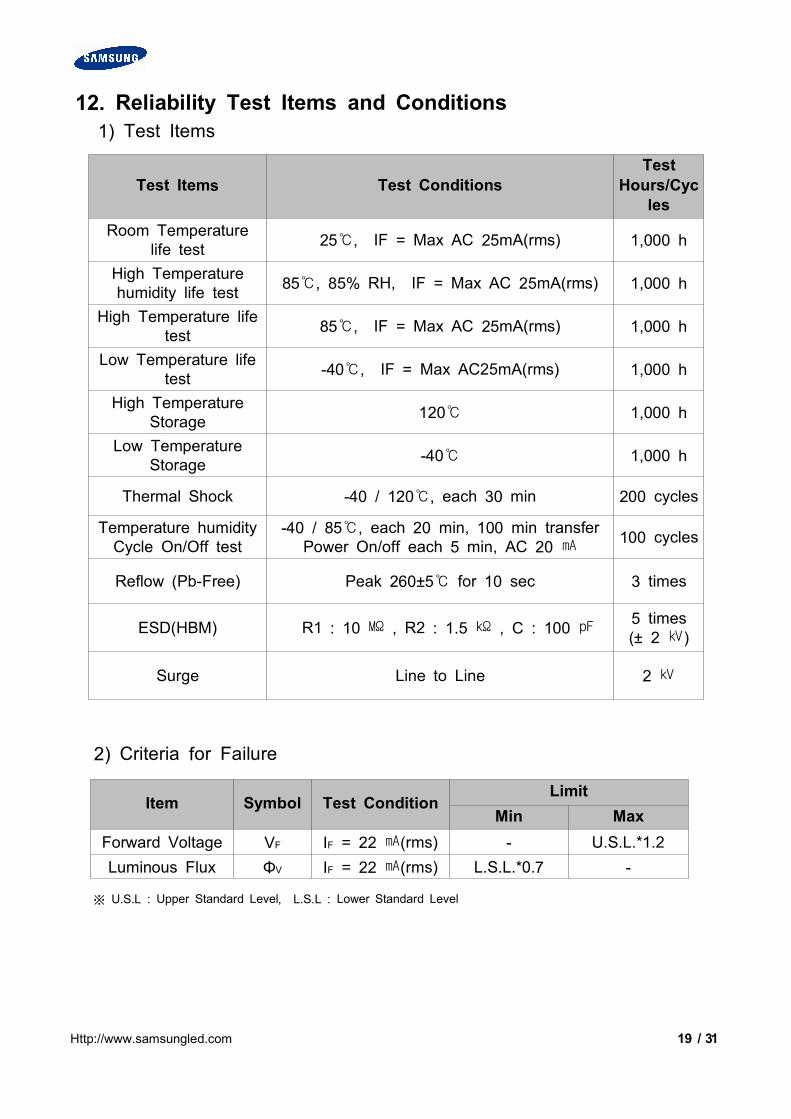
12. Reliability Test Items and Conditions1) Test Items
2) Criteria for Failure
Item Symbol Test ConditionLimit
Min MaxForward Voltage VF IF = 22 (rms) - U.S.L.*1.2Luminous Flux ΦV IF = 22 (rms) L.S.L.*0.7 -
※ U.S.L : Upper Standard Level, L.S.L : Lower Standard Level
Test Items Test ConditionsTest
Hours/Cycles
Room Temperaturelife test 25, IF = Max AC 25mA(rms) 1,000 h
High Temperaturehumidity life test 85, 85% RH, IF = Max AC 25mA(rms) 1,000 h
High Temperature lifetest 85, IF = Max AC 25mA(rms) 1,000 h
Low Temperature lifetest -40, IF = Max AC25mA(rms) 1,000 h
High TemperatureStorage 120 1,000 h
Low TemperatureStorage -40 1,000 h
Thermal Shock -40 / 120, each 30 min 200 cycles
Temperature humidityCycle On/Off test
-40 / 85, each 20 min, 100 min transferPower On/off each 5 min, AC 20
100 cycles
Reflow (Pb-Free) Peak 260±5 for 10 sec 3 times
ESD(HBM) R1 : 10 , R2 : 1.5 , C : 100 5 times(± 2 )
Surge Line to Line 2
20 / 31Http://www.samsungled.com
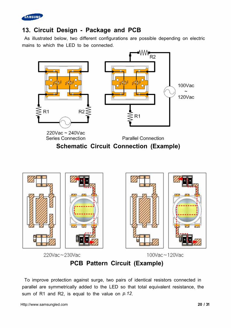
13. Circuit Design - Package and PCBAs illustrated below, two different configurations are possible depending on electricmains to which the LED to be connected.
Schematic Circuit Connection (Example)
PCB Pattern Circuit (Example)
To improve protection against surge, two pairs of identical resistors connected inparallel are symmetrically added to the LED so that total equivalent resistance, thesum of R1 and R2, is equal to the value on p.12.
21 / 31Http://www.samsungled.com
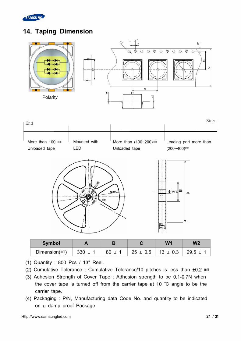
14. Taping Dimension
(1) Quantity : 800 Pcs / 13" Reel.(2) Cumulative Tolerance : Cumulative Tolerance/10 pitches is less than ±0.2
(3) Adhesion Strength of Cover Tape : Adhesion strength to be 0.1-0.7N whenthe cover tape is turned off from the carrier tape at 10 angle to be thecarrier tape.
(4) Packaging : P/N, Manufacturing data Code No. and quantity to be indicatedon a damp proof Package
More than 100
Unloaded tapeMounted withLED
Leading part more than(200~400)
More than (100~200)Unloaded tape
EndStart
Polarity
Symbol A B C W1 W2
Dimension() 330 ± 1 80 ± 1 25 ± 0.5 13 ± 0.3 29.5 ± 1
22 / 31Http://www.samsungled.com
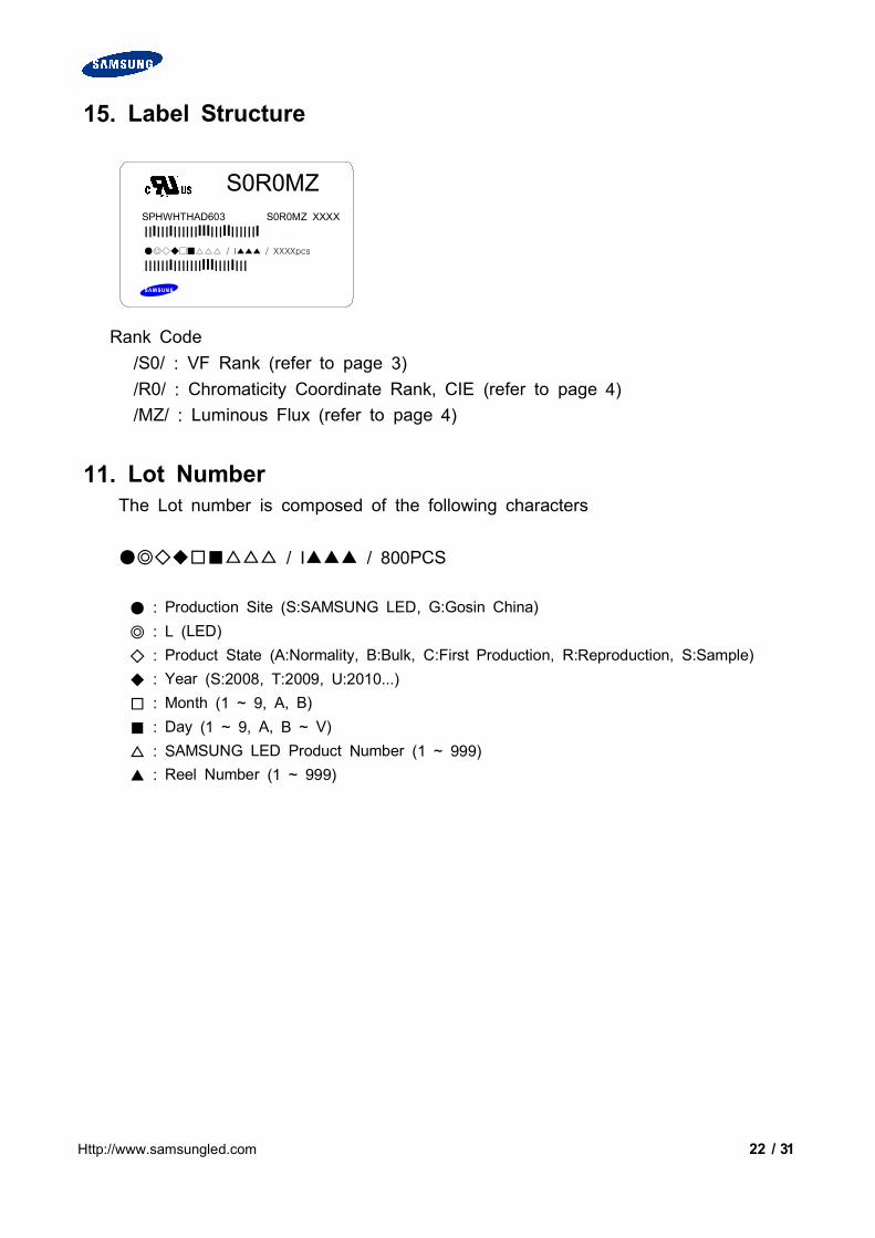
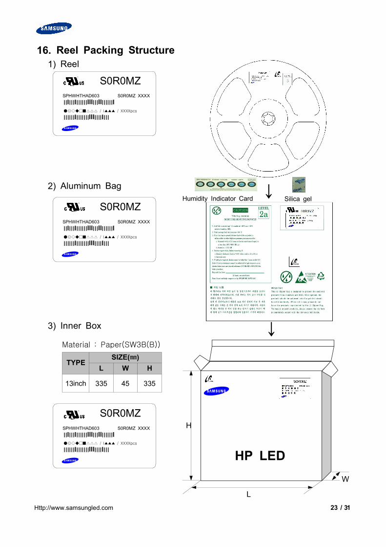
15. Label Structure
Rank Code/S0/ : VF Rank (refer to page 3)/R0/ : Chromaticity Coordinate Rank, CIE (refer to page 4)/MZ/ : Luminous Flux (refer to page 4)
11. Lot NumberThe Lot number is composed of the following characters
/ I / 800PCS
: Production Site (S:SAMSUNG LED, G:Gosin China) : L (LED) : Product State (A:Normality, B:Bulk, C:First Production, R:Reproduction, S:Sample) : Year (S:2008, T:2009, U:2010...) : Month (1 ~ 9, A, B) : Day (1 ~ 9, A, B ~ V) : SAMSUNG LED Product Number (1 ~ 999) : Reel Number (1 ~ 999)
S0R0MZSPHWHTHAD603 S0R0MZ XXXXIIIIIIIIIIIIIIIIIIIIIIIIIIII / I / XXXXpcs
IIIIIIIIIIIIIIIIIIIIIIIII
23 / 31Http://www.samsungled.com
16. Reel Packing Structure1) Reel
2) Aluminum Bag
3) Inner Box
HP LED
Material : Paper(SW3B(B))
TYPESIZE()
L W H
13inch 335 45 335
↓
↓ Silica gelHumidity Indicator Card
H
L
W
S0R0MZSPHWHTHAD603 S0R0MZ XXXXIIIIIIIIIIIIIIIIIIIIIIIIIIII / I / XXXXpcs
IIIIIIIIIIIIIIIIIIIIIIIII
S0R0MZSPHWHTHAD603 S0R0MZ XXXXIIIIIIIIIIIIIIIIIIIIIIIIIIII / I / XXXXpcs
IIIIIIIIIIIIIIIIIIIIIIIII
S0R0MZSPHWHTHAD603 S0R0MZ XXXXIIIIIIIIIIIIIIIIIIIIIIIIIIII / I / XXXXpcs
IIIIIIIIIIIIIIIIIIIIIIIII
24 / 31Http://www.samsungled.com
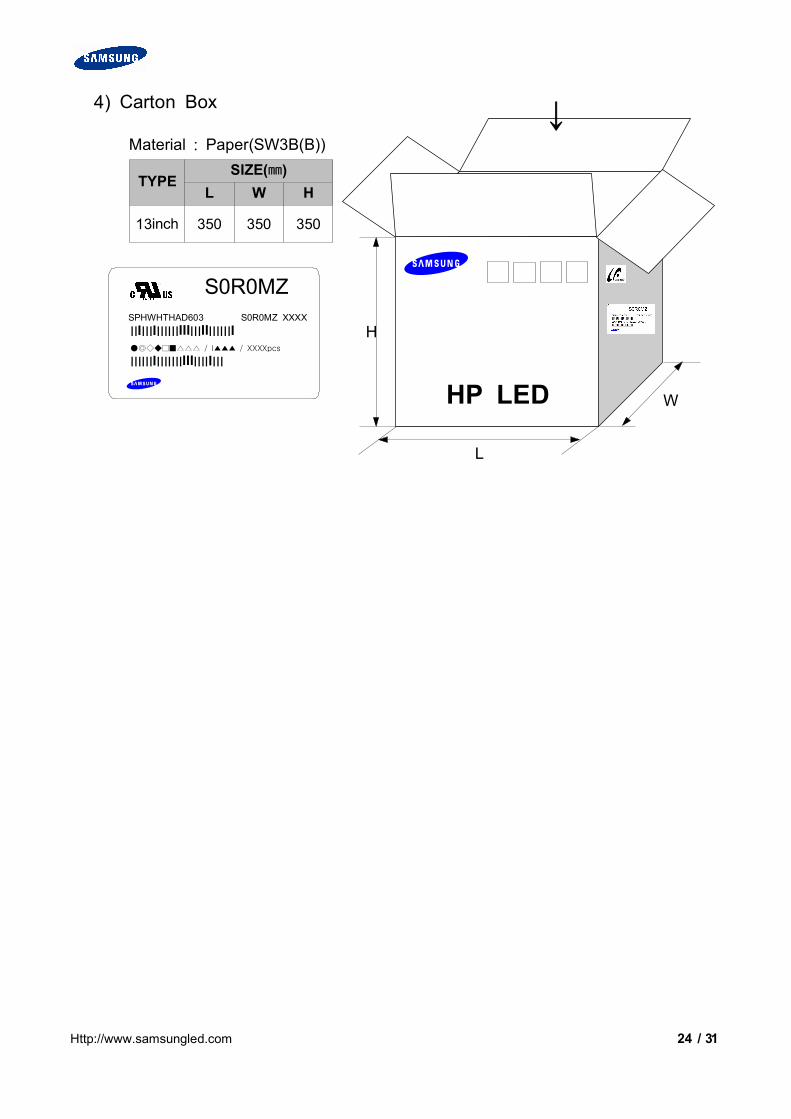
4) Carton Box
Material : Paper(SW3B(B))
TYPESIZE()
L W H
13inch 350 350 350
HP LED
↓
L
W
H
S0R0MZSPHWHTHAD603 S0R0MZ XXXXIIIIIIIIIIIIIIIIIIIIIIIIIIII / I / XXXXpcs
IIIIIIIIIIIIIIIIIIIIIIIII

25 / 31Http://www.samsungled.com
17. Aluminum Packing Bag
Silica gel & Humidity Indicator Card in Aluminum Packing Bag
26 / 31Http://www.samsungled.com
18. Precaution for Use
1) For over-current-proof function, customers are recommended to applyresistors to prevent sudden change of the current caused by slight shift ofthe voltage.
2) This device should not be used in any type of fluid such as water, oil,organic solvent, etc. When washing is required, IPA is recommended to use.
3) When the LEDs illuminate, operating current should be decided afterconsidering the ambient maximum temperature.
4) LEDs must be stored in a clean environment. If the LEDs are to be storedfor 3 months or more after being shipped from SAMSUNG LED, they shouldbe packed by a sealed container with nitrogen gas injected. (Shelf life ofsealed bags : 12 months, temp. 0~40, 20~70%RH)
5) After storage bag is open, device subjected to soldering, solder reflow, orother high temperature processes must be:a. Mounted within 168 hours (7days) at an assembly line with a condition
of no more than 30/60%RH,b. Stored at <10% RH.
6) Repack unused Products with anti-moisture packing, fold to close anyopening and then store in a dry place.
7) Devices require baking before mounting, if humidity card reading is >60% at23±5.
8) Devices must be baked for 24hours at 65±5, if baking is required.
9) The LEDs are sensitive to the static electricity and surge. It isrecommended to use a wrist band or anti-electrostatic glove when handlingthe LEDs.If voltage exceeding the absolute maximum rating is applied to LEDs, it maycause damage or even destruction to LED devices.Damaged LEDs may show some unusual characteristics such as increase inleak current, lowered turn-on voltage, or abnormal lighting of LEDs at lowcurrent.
27 / 31Http://www.samsungled.com
10) When handling LED with tweezers, the LED Should only be held by thepolymer body, not by the encapsulant or LENS.
11) The use of appropriate nozzle for the LED recommended. For therecommended nozzle size, refer to the figure at the below.Inner diameter of nozzle ≥ Φ9.2mm
12) Do not stack assembled PCBs together. Since silicone is a soft material,abrasion between two PCB assembled with silicone encapsulated LED mightcause catastrophic failure of the LEDs due to damage to encapsulant andwire and LED detachment.
28 / 31Http://www.samsungled.com
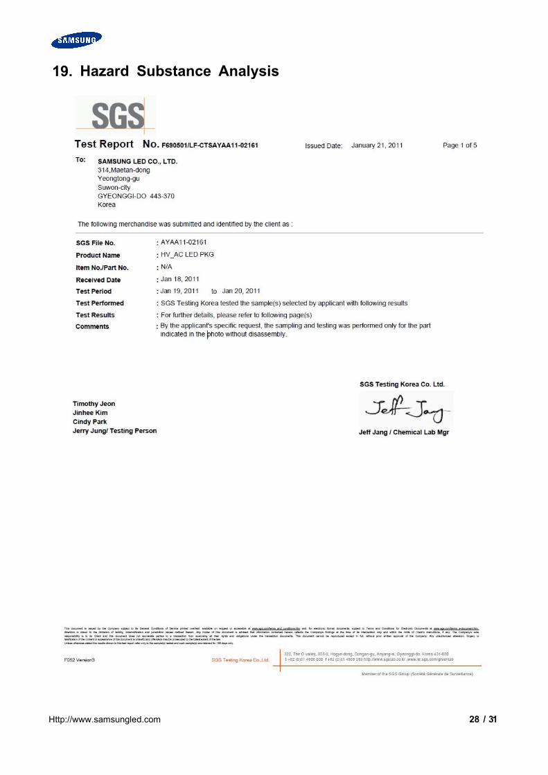
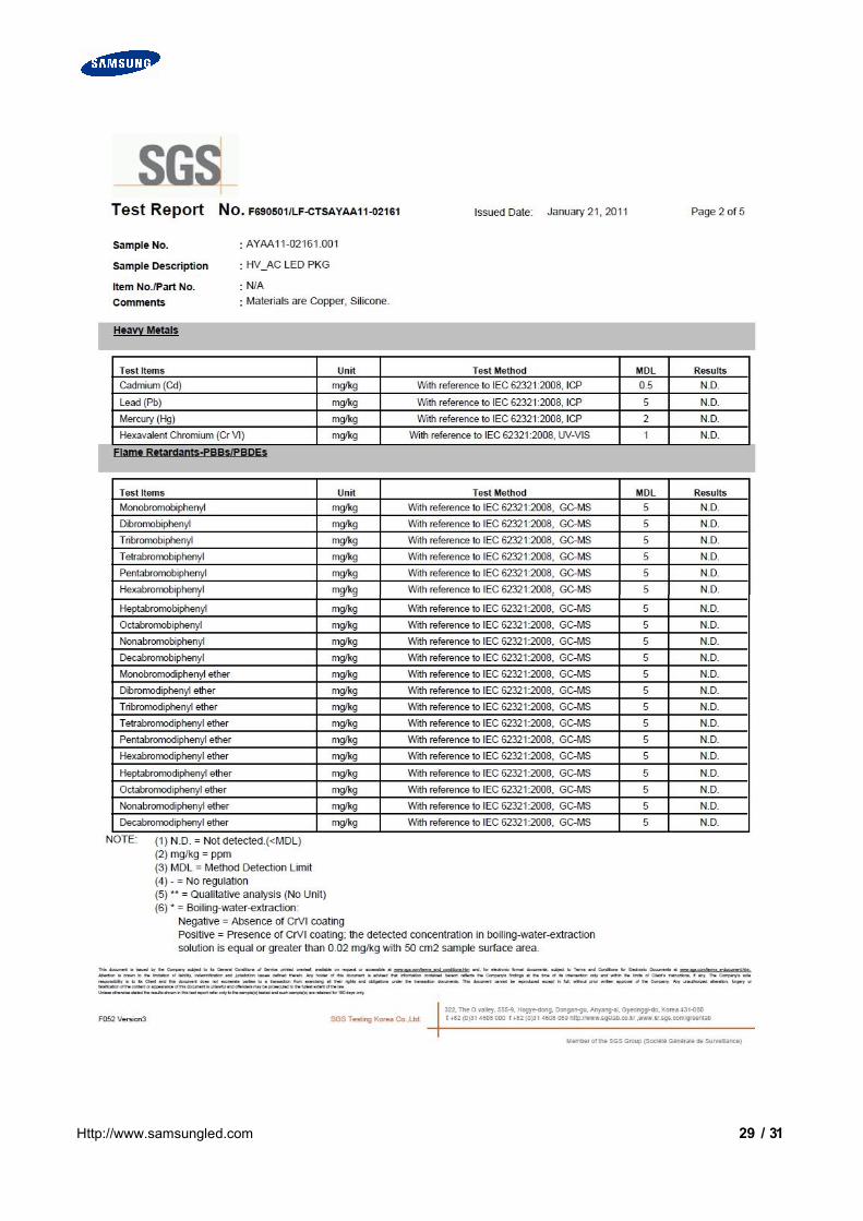
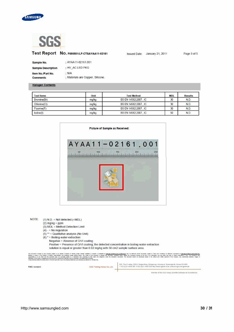
19. Hazard Substance Analysis
29 / 31Http://www.samsungled.com
30 / 31Http://www.samsungled.com
31 / 31Http://www.samsungled.com
Date Revision HistoryAuthor
Drawn Approved2012.10.25 Initial Edition of Product Family Data sheet I.S. Park M.Y. Son
2012.10.26 Updated mechanical dimensions and detailson lens shape on p.17 I.S. Park M.Y. Son
Revision History