ISL84051, ISL84052, ISL84053 Datasheet - Intersil.com ISL84052, ISL84053 Low Voltage, Single and...
19
FN6047 Rev.10.00 Page 1 of 19 May 16, 2011 FN6047 Rev.10.00 May 16, 2011 ISL84051, ISL84052, ISL84053 Low Voltage, Single and Dual Supply, 8-to-1 Multiplexer, Dual 4-to-1 Multiplexer and a Triple SPDT Analog Switch DATASHEET The Intersil ISL84051, ISL84052, ISL84053 devices are precision, bidirectional, analog switches configured as a 8-Channel multiplexer/demultiplexer (ISL84051), a dual differential 4-Channel multiplexer/demultiplexer (ISL84052) and a triple single pole/double throw (SPDT) switch (ISL84053) designed to operate from a single +2V to +12V supply or from a ±2V to ±6V supply. All devices have an inhibit pin to simultaneously open all signal paths. ON-resistance is 60Ω with a ±5V supply and 125Ω with a single +5V supply. Each switch can handle rail to rail analog signals. The off-leakage current is only 5nA at +85°C with a ±5V supply. All digital inputs have 0.8V to 2.4V logic thresholds, ensuring TTL/CMOS logic compatibility when using a single +3.3V and +5V supply or dual ±5V supplies. The ISL84051 is a 8-to-1 multiplexer device. The ISL84052 is a dual 4-to-1 multiplexer device. The ISL84053 is a committed triple SPDT, which is perfect for use in 2-to-1 multiplexer applications. Table 1 summarizes the performance of this family. Related Literature • Technical Brief TB363 “Guidelines for Handling and Processing Moisture Sensitive Surface Mount Devices (SMDs)” • Application Note AN557 “Recommended Test Procedures for Analog Switches” Features • Drop-in Replacements for MAX4051/MAX4051A, MAX4052/MAX4052A and MAX4053/MAX4053A • Pin Compatible with MAX4581, MAX4582, MAX4583 and with Industry Standard 74HC4051, 74HC4052 and 74HC4053 • ON-Resistance (r ON ) Max, V S = ±5V . . . . . . . . . . . . . . . . . 100Ω • ON-Resistance (r ON ) Max, V S = +5V . . . . . . . . . . . . . . . . . 225Ω •r ON Matching Between Channels . . . . . . . . . . . . . . . . . . . . . . <6Ω • Low Charge Injection . . . . . . . . . . . . . . . . . . . . . . . . . . . . . . . . . 2pC • Single Supply Operation. . . . . . . . . . . . . . . . . . . . . . . +2V to +12V • Dual Supply Operation . . . . . . . . . . . . . . . . . . . . . . . . . . ±2V to ±6 • Fast Switching Action (V S = +5V) - t ON . . . . . . . . . . . . . . . . . . . . . . . . . . . . . . . . . . . . . . . . . 90ns - t OFF . . . . . . . . . . . . . . . . . . . . . . . . . . . . . . . . . . . . . . . . . 60ns • Guaranteed Max Off-leakage @ V S = ±5V . . . . . . . . . . . . . . 5nA • Break-Before-Make • TTL, CMOS Compatible • Pb-Free Available (RoHS Compliant) Applications • Portable Equipment • Communications Systems - Radios - Telecom Infrastructure - ADSL, VDSL Modems • Test Equipment - Medical Ultrasound - Magnetic Resonance Image - CT and PET Scanners (MRI) - ATE - Electrocardiograph • Audio and Video Signal Routing • Various Circuits - +3V/+5V DACs and ADCs - Sample and Hold Circuits - Operational Amplifier Gain Switching Networks - High Frequency Analog Switching - High Speed Multiplexing - Integrator Reset Circuits TABLE 1. FEATURES AT A GLANCE CONFIGURATION ISL84051 ISL84052 ISL84053 8:1 Mux DUAL 4:1 Mux TRIPLE SPDT ±5V r ON 60Ω 60Ω 60Ω ±5V t ON /t OFF 50ns/40ns 50ns/40ns 50ns/40ns 5V r ON 125Ω 125Ω 125Ω 5V t ON /t OFF 90ns/60ns 90ns/60ns 90ns/60ns 3V r ON 250Ω 250Ω 250Ω 3V t ON /t OFF 180ns/100ns 180ns/100ns 180ns/100ns Packages 16 Ld SOIC 16 Ld SOIC 16 Ld SOIC 16 Ld QSOP 16 Ld QSOP 16 Ld QSOP 16 Ld TSSOP 16 Ld TSSOP 16 Ld TSSOP
Transcript of ISL84051, ISL84052, ISL84053 Datasheet - Intersil.com ISL84052, ISL84053 Low Voltage, Single and...

FN6047Rev.10.00
May 16, 2011
ISL84051, ISL84052, ISL84053Low Voltage, Single and Dual Supply, 8-to-1 Multiplexer, Dual 4-to-1 Multiplexer and a Triple SPDT Analog Switch
DATASHEET
The Intersil ISL84051, ISL84052, ISL84053 devices are precision, bidirectional, analog switches configured as a 8-Channel multiplexer/demultiplexer (ISL84051), a dual differential 4-Channel multiplexer/demultiplexer (ISL84052) and a triple single pole/double throw (SPDT) switch (ISL84053) designed to operate from a single +2V to +12V supply or from a ±2V to ±6V supply. All devices have an inhibit pin to simultaneously open all signal paths.
ON-resistance is 60Ω with a ±5V supply and 125Ω with a single +5V supply. Each switch can handle rail to rail analog signals. The off-leakage current is only 5nA at +85°C with a ±5V supply.
All digital inputs have 0.8V to 2.4V logic thresholds, ensuring TTL/CMOS logic compatibility when using a single +3.3V and +5V supply or dual ±5V supplies.
The ISL84051 is a 8-to-1 multiplexer device. The ISL84052 is a dual 4-to-1 multiplexer device. The ISL84053 is a committed triple SPDT, which is perfect for use in 2-to-1 multiplexer applications.
Table 1 summarizes the performance of this family.
Related Literature• Technical Brief TB363 “Guidelines for Handling and
Processing Moisture Sensitive Surface Mount Devices (SMDs)”
• Application Note AN557 “Recommended Test Procedures for Analog Switches”
Features• Drop-in Replacements for MAX4051/MAX4051A,
MAX4052/MAX4052A and MAX4053/MAX4053A
• Pin Compatible with MAX4581, MAX4582, MAX4583 and with Industry Standard 74HC4051, 74HC4052 and 74HC4053
• ON-Resistance (rON) Max, VS = ±5V. . . . . . . . . . . . . . . . . 100Ω
• ON-Resistance (rON) Max, VS = +5V. . . . . . . . . . . . . . . . . 225Ω
• rON Matching Between Channels . . . . . . . . . . . . . . . . . . . . . . <6Ω
• Low Charge Injection . . . . . . . . . . . . . . . . . . . . . . . . . . . . . . . . . 2pC
• Single Supply Operation. . . . . . . . . . . . . . . . . . . . . . . +2V to +12V
• Dual Supply Operation . . . . . . . . . . . . . . . . . . . . . . . . . . ±2V to ±6
• Fast Switching Action (VS = +5V)
- tON . . . . . . . . . . . . . . . . . . . . . . . . . . . . . . . . . . . . . . . . . 90ns
- tOFF . . . . . . . . . . . . . . . . . . . . . . . . . . . . . . . . . . . . . . . . . 60ns
• Guaranteed Max Off-leakage @ VS = ±5V . . . . . . . . . . . . . . 5nA
• Break-Before-Make
• TTL, CMOS Compatible
• Pb-Free Available (RoHS Compliant)
Applications• Portable Equipment
• Communications Systems
- Radios
- Telecom Infrastructure
- ADSL, VDSL Modems
• Test Equipment
- Medical Ultrasound
- Magnetic Resonance Image
- CT and PET Scanners (MRI)
- ATE
- Electrocardiograph
• Audio and Video Signal Routing
• Various Circuits
- +3V/+5V DACs and ADCs
- Sample and Hold Circuits
- Operational Amplifier Gain Switching Networks
- High Frequency Analog Switching
- High Speed Multiplexing
- Integrator Reset Circuits
TABLE 1. FEATURES AT A GLANCE
CONFIGURATION
ISL84051 ISL84052 ISL84053
8:1 MuxDUAL
4:1 Mux TRIPLE SPDT
±5V rON 60Ω 60Ω 60Ω
±5V tON/tOFF 50ns/40ns 50ns/40ns 50ns/40ns
5V rON 125Ω 125Ω 125Ω
5V tON/tOFF 90ns/60ns 90ns/60ns 90ns/60ns
3V rON 250Ω 250Ω 250Ω
3V tON/tOFF 180ns/100ns 180ns/100ns 180ns/100ns
Packages 16 Ld SOIC 16 Ld SOIC 16 Ld SOIC
16 Ld QSOP 16 Ld QSOP 16 Ld QSOP
16 Ld TSSOP 16 Ld TSSOP 16 Ld TSSOP
FN6047 Rev.10.00 Page 1 of 19May 16, 2011

ISL84051, ISL84052, ISL84053
Pin ConfigurationsISL84051
(16 LD SOIC, QSOP, TSSOP)TOP VIEW
ISL84052(16 LD SOIC, QSOP, TSSOP)
TOP VIEW
ISL84053(16 LD SOIC, QSOP, TSSOP)
TOP VIEW
NOTE:1. Switches Shown for Logic “0” Inputs.
14
15
16
9
13
12
11
10
1
2
3
4
5
7
6
8
NO1
NO3
COM
NO7
NO5
INH
GND
V-
V+
NO4
NO0
NO6
ADDC
ADDB
ADDA
NO2
LOGIC
14
15
16
9
13
12
11
10
1
2
3
4
5
7
6
8
NO0B
NO1B
COMB
NO3B
NO2B
INH
GND
V-
V+
NO2A
COMA
NO0A
NO3A
ADDB
ADDA
NO1A
LOGIC
14
15
16
9
13
12
11
10
1
2
3
4
5
7
6
8
NOB
NCB
NOA
COMA
NCA
INH
GND
V-
V+
COMC
NOC
NCC
ADDC
ADDB
ADDA
COMB
Pin Description
PIN NAME
PIN NUMBER
FUNCTIONISL84051 ISL84052 ISL84053
V+ 16 16 16 Positive Power Supply Input
V- 7 7 7 Negative Power Supply Input. Connect to GND for Single Supply Configurations.
GND 8 8 8 Ground Connection
INH 6 6 6 Digital Control Input. Connect to GND for Normal Operation. Connect to V+ to turn all switches off.
COM 3 - - Analog Switch Common Pin
COMA - 13 4
COMB - 3 15
COMC - - 14
NO1, NO3, NO7, NO5,
NO6, NO4, NO2
1, 2,4, 5,
12, 14, 15
- - Analog Switch Normally Open Pin
FN6047 Rev.10.00 Page 2 of 19May 16, 2011

ISL84051, ISL84052, ISL84053
NO0B, NO1B, NO3B, NO2B, NO3A, NO0A, NO2A, NO1A
- 1, 2,4, 5,
11, 12,14, 15
- Analog Switch Normally Open Pin
NOB, NOA, NOC - - 1, 3, 13
NCB, NCA, NCC - - 2, 5, 12 Analog Switch Normally Closed Pin
ADDA, ADDB, ADDC
9, 1011
9, 10-
9, 1011
Address Input Pin
Pin Description (Continued)
PIN NAME
PIN NUMBER
FUNCTIONISL84051 ISL84052 ISL84053
Ordering InformationPART
NUMBERPART
MARKINGTEMP. RANGE
(°C)PACKAGE(Pb-free)
PKG. DWG. #
ISL84051IAZ 84051 IAZ -40 to +85 16 Ld QSOP M16.15A
ISL84051IBZ 84051IBZ -40 to +85 16 Ld SOIC M16.15
ISL84051IVZ 84051 IVZ -40 to +85 16 Ld TSSOP M16.173
ISL84052IAZ 84052 IAZ -40 to +85 16 Ld QSOP M16.15A
ISL84052IBZ 84052IBZ -40 to +85 16 Ld SOIC M16.15
ISL84052IVZ 84052 IVZ -40 to +85 16 Ld TSSOP M16.173
ISL84053IAZ 84053 IAZ -40 to +85 16 Ld QSOP M16.15A
ISL84053IBZ 84053IBZ -40 to +85 16 Ld SOIC M16.15
ISL84053IVZ 84053 IVZ -40 to +85 16 Ld TSSOP M16.173
NOTES:
2. Add “-T*” suffix for tape and reel. Please refer to TB347 for details on reel specifications.
3. These Intersil Pb-free plastic packaged products employ special Pb-free material sets, molding compounds/die attach materials, and 100% matte tin plate plus anneal (e3 termination finish, which is RoHS compliant and compatible with both SnPb and Pb-free soldering operations). Intersil Pb-free products are MSL classified at Pb-free peak reflow temperatures that meet or exceed the Pb-free requirements of IPC/JEDEC J STD-020
4. For Moisture Sensitivity Level (MSL), please see device information page for ISL84051, ISL84052, ISL84053. For more information on MSL please see techbrief TB363.
FN6047 Rev.10.00 Page 3 of 19May 16, 2011

ISL84051, ISL84052, ISL84053
Truth TablesISL84051
INH ADDC ADDB ADDASWITCH
ON
1 X X X None
0 0 0 0 NO0
0 0 0 1 NO1
0 0 1 0 NO2
0 0 1 1 NO3
0 1 0 0 NO4
0 1 0 1 NO5
0 1 1 0 NO6
0 1 1 1 NO7
ISL84052
INH ADDB ADDA SWITCH ON
1 X X None
0 0 0 NO0
0 0 1 NO1
0 1 0 NO2
0 1 1 NO3
ISL84053
INH ADDC ADDB ADDA SWITCH ON
1 X X X None
0 X X 0 NCA
0 X X 1 NOA
0 X 0 X NCB
0 X 1 X NOB
0 0 X X NCC
0 1 X X NOC
NOTE: Logic “0” ≤0.8V. Logic “1” ≥2.4V, with V+ between 2.7V and 10V. X = Don’t Care.
FN6047 Rev.10.00 Page 4 of 19May 16, 2011

ISL84051, ISL84052, ISL84053
Absolute Maximum Ratings Thermal InformationV+ to V-. . . . . . . . . . . . . . . . . . . . . . . . . . . . . . . . . . . . . . . . . . . . . -0.3V to 15VV+ to GND . . . . . . . . . . . . . . . . . . . . . . . . . . . . . . . . . . . . . . . . . . -0.3V to 15VV- to GND . . . . . . . . . . . . . . . . . . . . . . . . . . . . . . . . . . . . . . . . . . . -15V to 0.3VInput Voltages
INH, NO, NC, ADD (Note 5). . . . . . . . . . . . . . . . ((V-) - 0.3) to ((V+) + 0.3V)Output Voltages
COM (Note 5). . . . . . . . . . . . . . . . . . . . . . . . . . . ((V-) - 0.3) to ((V+) + 0.3V)Continuous Current (Any Terminal) . . . . . . . . . . . . . . . . . . . . . . . . . . ±30mA
Peak Current NO, NC, or COM (Pulsed 1ms, 10% Duty Cycle, Max). . . . . . . . . . . . . . . . . . . . . . . . ±100mAESD Rating
Human Body Model (Per MIL-STD-883, Method 3015.7) . . . . . . . . >2kV
Thermal Resistance (Typical, Notes 6, 7) JA (°C/W) JC (°C/W)16 Ld SOIC Package . . . . . . . . . . . . . . . . . . 75 3916 Ld QSOP Package. . . . . . . . . . . . . . . . . . 95 5616 Ld TSSOP Package . . . . . . . . . . . . . . . . . 110 33
Maximum Junction Temperature (Plastic Package) . . . . . . . . . . . +150°CMaximum Storage Temperature Range. . . . . . . . . . . . . . . . . -65°C to +150°CPb-Free Reflow Profile . . . . . . . . . . . . . . . . . . . . . . . . . . . . . . . see link below
http://www.intersil.com/pbfree/Pb-FreeReflow.asp
Operating ConditionsTemperature Range . . . . . . . . . . . . . . . . . . . . . . . . . . . . . . . -40°C to +85°C
CAUTION: Do not operate at or near the maximum ratings listed for extended periods of time. Exposure to such conditions may adversely impact productreliability and result in failures not covered by warranty.
NOTES:
5. Signals on NC, NO, COM, ADD, or INH exceeding V+ or V- are clamped by internal diodes. Limit forward diode current to maximum current ratings.
6. JA is measured with the component mounted on a high effective thermal conductivity test board in free air. See Tech Brief TB379 for details.
7. For JC, the “case temp” location is taken at the package top center.
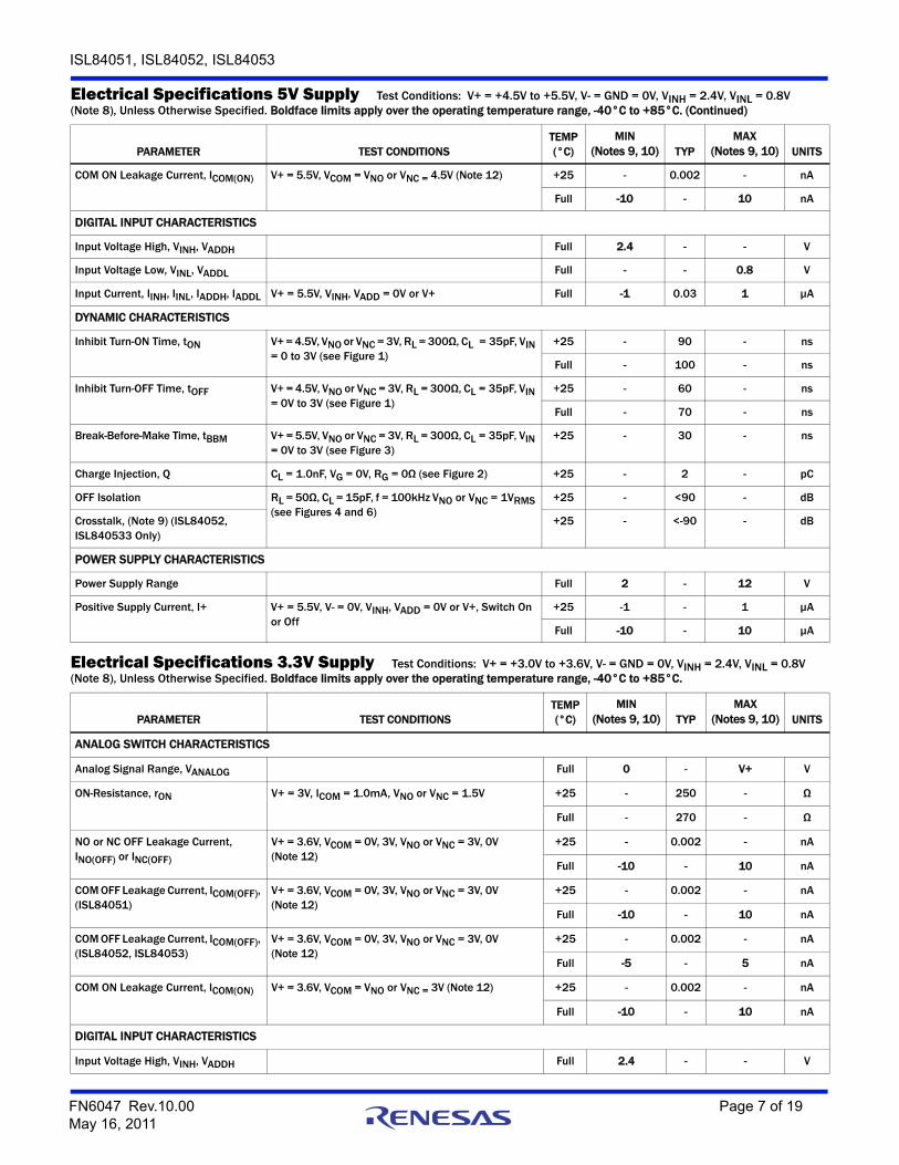
Electrical Specifications 5V Supply Test Conditions: VSUPPLY = ±4.5V to ±5.5V, GND = 0V, VINH = 2.4V, VINL = 0.8V (Note 8), Unless Otherwise Specified. Boldface limits apply over the operating temperature range, -40°C to +85°C.
PARAMETER TEST CONDITIONSTEMP(°C)
MIN(Notes 9, 10) TYP
MAX(Notes 9, 10) UNITS
ANALOG SWITCH CHARACTERISTICS
Analog Signal Range, VANALOG Full V- - V+ V
ON-Resistance, rON VS = ±5V, ICOM = 1mA, VNO or VNC = ±3V(see Figure 5)
+25 - 60 100 Ω
Full - - 125 Ω
rON Matching Between Channels, rON
VS = ±5V, ICOM = 1mA, VNO or VNC = ±3V (Note 11) +25 - - 6 Ω
Full - - 12 Ω
rON Flatness, rFLAT(ON) VS = ±5V, ICOM = 1mA, VNO or VNC = ±3V, 0V(Note 12)
+25 - - 10 Ω
Full - - 15 Ω
NO or NC OFF Leakage Current, INO(OFF) or INC(OFF)
VS = ±5.5V, VCOM = ±4.5V, VNO or VNC = ±4.5V(Note 12)
+25 - 0.002 - nA
Full -5 - 5 nA
COM OFF Leakage Current, ICOM(OFF), (ISL84051)
VS = ±5.5V, VCOM = ±4.5V, VNO or VNC = ±4.5V(Note 12)
+25 - 0.002 - nA
Full -5 - 5 nA
COM OFF Leakage Current, ICOM(OFF), (ISL84052, ISL84053)
VS = ±5.5V, VCOM = ±4.5V, VNO or VNC = ±4.5V(Note 12)
+25 - 0.002 - nA
Full -2.5 - 2.5 nA
COM ON Leakage Current, ICOM(ON), (ISL84051)
VS = ±5.5V, VCOM = VNO or VNC = ±4.5V(Note 12)
+25 - 0.002 - nA
Full -5 - 5 nA
COM ON Leakage Current, ICOM(ON), (ISL84052, ISL84053)
VS = ±5.5V, VCOM = VNO or VNC = ±4.5V (Note 12) +25 - 0.002 - nA
Full -2.5 - 2.5 nA
DIGITAL INPUT CHARACTERISTICS
Input Voltage High, VINH, VADDH Full 2.4 - - V
Input Voltage Low, VINL, VADDL Full - - 0.8 V
Input Current, IINH, IINL, IADDH, IADDL VS = ±5.5V, VINH, VADD = 0V or V+ Full -1 0.03 1 µA
FN6047 Rev.10.00 Page 5 of 19May 16, 2011
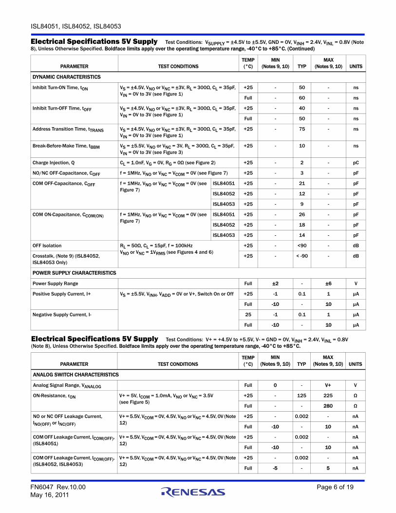
ISL84051, ISL84052, ISL84053
DYNAMIC CHARACTERISTICS
Inhibit Turn-ON Time, tON VS = ±4.5V, VNO or VNC = ±3V, RL = 300Ω, CL = 35pF, VIN = 0V to 3V (see Figure 1)
+25 - 50 - ns
Full - 60 - ns
Inhibit Turn-OFF Time, tOFF VS = ±4.5V, VNO or VNC = ±3V, RL = 300Ω, CL = 35pF, VIN = 0V to 3V (see Figure 1)
+25 - 40 - ns
Full - 50 - ns
Address Transition Time, tTRANS VS = ±4.5V, VNO or VNC = ±3V, RL = 300Ω, CL = 35pF, VIN = 0V to 3V (see Figure 1)
+25 - 75 - ns
Break-Before-Make Time, tBBM VS = ±5.5V, VNO or VNC = 3V, RL = 300Ω, CL = 35pF, VIN = 0V to 3V (see Figure 3)
+25 - 10 - ns
Charge Injection, Q CL = 1.0nF, VG = 0V, RG = 0Ω (see Figure 2) +25 - 2 - pC
NO/NC OFF-Capacitance, COFF f = 1MHz, VNO or VNC = VCOM = 0V (see Figure 7) +25 - 3 - pF
COM OFF-Capacitance, COFF f = 1MHz, VNO or VNC = VCOM = 0V (see Figure 7)
ISL84051 +25 - 21 - pF
ISL84052 +25 - 12 - pF
ISL84053 +25 - 9 - pF
COM ON-Capacitance, CCOM(ON) f = 1MHz, VNO or VNC = VCOM = 0V (see Figure 7)
ISL84051 +25 - 26 - pF
ISL84052 +25 - 18 - pF
ISL84053 +25 - 14 - pF
OFF Isolation RL = 50Ω, CL = 15pF, f = 100kHzVNO or VNC = 1VRMS (see Figures 4 and 6)
+25 - <90 - dB
Crosstalk, (Note 9) (ISL84052, ISL84053 Only)
+25 - < -90 - dB
POWER SUPPLY CHARACTERISTICS
Power Supply Range Full ±2 - ±6 V
Positive Supply Current, I+ VS = ±5.5V, VINH, VADD = 0V or V+, Switch On or Off +25 -1 0.1 1 µA
Full -10 - 10 µA
Negative Supply Current, I- 25 -1 0.1 1 µA
Full -10 - 10 µA
Electrical Specifications 5V Supply Test Conditions: V+ = +4.5V to +5.5V, V- = GND = 0V, VINH = 2.4V, VINL = 0.8V (Note 8), Unless Otherwise Specified. Boldface limits apply over the operating temperature range, -40°C to +85°C.
PARAMETER TEST CONDITIONSTEMP(°C)
MIN(Notes 9, 10) TYP
MAX(Notes 9, 10) UNITS
ANALOG SWITCH CHARACTERISTICS
Analog Signal Range, VANALOG Full 0 - V+ V
ON-Resistance, rON V+ = 5V, ICOM = 1.0mA, VNO or VNC = 3.5V(see Figure 5)
+25 - 125 225 Ω
Full - - 280 Ω
NO or NC OFF Leakage Current, INO(OFF) or INC(OFF)
V+ = 5.5V, VCOM = 0V, 4.5V, VNO or VNC = 4.5V, 0V (Note 12)
+25 - 0.002 - nA
Full -10 - 10 nA
COM OFF Leakage Current, ICOM(OFF), (ISL84051)
V+ = 5.5V, VCOM = 0V, 4.5V, VNO or VNC = 4.5V, 0V (Note 12)
+25 - 0.002 - nA
Full -10 - 10 nA
COM OFF Leakage Current, ICOM(OFF), (ISL84052, ISL84053)
V+ = 5.5V, VCOM = 0V, 4.5V, VNO or VNC = 4.5V, 0V (Note 12)
+25 - 0.002 - nA
Full -5 - 5 nA
Electrical Specifications 5V Supply Test Conditions: VSUPPLY = ±4.5V to ±5.5V, GND = 0V, VINH = 2.4V, VINL = 0.8V (Note 8), Unless Otherwise Specified. Boldface limits apply over the operating temperature range, -40°C to +85°C. (Continued)
PARAMETER TEST CONDITIONSTEMP(°C)
MIN(Notes 9, 10) TYP
MAX(Notes 9, 10) UNITS
FN6047 Rev.10.00 Page 6 of 19May 16, 2011
ISL84051, ISL84052, ISL84053
COM ON Leakage Current, ICOM(ON) V+ = 5.5V, VCOM = VNO or VNC = 4.5V (Note 12) +25 - 0.002 - nA
Full -10 - 10 nA
DIGITAL INPUT CHARACTERISTICS
Input Voltage High, VINH, VADDH Full 2.4 - - V
Input Voltage Low, VINL, VADDL Full - - 0.8 V
Input Current, IINH, IINL, IADDH, IADDL V+ = 5.5V, VINH, VADD = 0V or V+ Full -1 0.03 1 µA
DYNAMIC CHARACTERISTICS
Inhibit Turn-ON Time, tON V+ = 4.5V, VNO or VNC = 3V, RL = 300Ω, CL = 35pF, VIN = 0 to 3V (see Figure 1)
+25 - 90 - ns
Full - 100 - ns
Inhibit Turn-OFF Time, tOFF V+ = 4.5V, VNO or VNC = 3V, RL = 300Ω, CL = 35pF, VIN = 0V to 3V (see Figure 1)
+25 - 60 - ns
Full - 70 - ns
Break-Before-Make Time, tBBM V+ = 5.5V, VNO or VNC = 3V, RL = 300Ω, CL = 35pF, VIN = 0V to 3V (see Figure 3)
+25 - 30 - ns
Charge Injection, Q CL = 1.0nF, VG = 0V, RG = 0Ω (see Figure 2) +25 - 2 - pC
OFF Isolation RL = 50Ω, CL = 15pF, f = 100kHz VNO or VNC = 1VRMS (see Figures 4 and 6)
+25 - <90 - dB
Crosstalk, (Note 9) (ISL84052, ISL840533 Only)
+25 - <-90 - dB
POWER SUPPLY CHARACTERISTICS
Power Supply Range Full 2 - 12 V
Positive Supply Current, I+ V+ = 5.5V, V- = 0V, VINH, VADD = 0V or V+, Switch On or Off
+25 -1 - 1 µA
Full -10 - 10 µA
Electrical Specifications 3.3V Supply Test Conditions: V+ = +3.0V to +3.6V, V- = GND = 0V, VINH = 2.4V, VINL = 0.8V (Note 8), Unless Otherwise Specified. Boldface limits apply over the operating temperature range, -40°C to +85°C.
PARAMETER TEST CONDITIONSTEMP(°C)
MIN(Notes 9, 10) TYP
MAX(Notes 9, 10) UNITS
ANALOG SWITCH CHARACTERISTICS
Analog Signal Range, VANALOG Full 0 - V+ V
ON-Resistance, rON V+ = 3V, ICOM = 1.0mA, VNO or VNC = 1.5V +25 - 250 - Ω
Full - 270 - Ω
NO or NC OFF Leakage Current, INO(OFF) or INC(OFF)
V+ = 3.6V, VCOM = 0V, 3V, VNO or VNC = 3V, 0V(Note 12)
+25 - 0.002 - nA
Full -10 - 10 nA
COM OFF Leakage Current, ICOM(OFF), (ISL84051)
V+ = 3.6V, VCOM = 0V, 3V, VNO or VNC = 3V, 0V(Note 12)
+25 - 0.002 - nA
Full -10 - 10 nA
COM OFF Leakage Current, ICOM(OFF), (ISL84052, ISL84053)
V+ = 3.6V, VCOM = 0V, 3V, VNO or VNC = 3V, 0V(Note 12)
+25 - 0.002 - nA
Full -5 - 5 nA
COM ON Leakage Current, ICOM(ON) V+ = 3.6V, VCOM = VNO or VNC = 3V (Note 12) +25 - 0.002 - nA
Full -10 - 10 nA
DIGITAL INPUT CHARACTERISTICS
Input Voltage High, VINH, VADDH Full 2.4 - - V
Electrical Specifications 5V Supply Test Conditions: V+ = +4.5V to +5.5V, V- = GND = 0V, VINH = 2.4V, VINL = 0.8V (Note 8), Unless Otherwise Specified. Boldface limits apply over the operating temperature range, -40°C to +85°C. (Continued)
PARAMETER TEST CONDITIONSTEMP(°C)
MIN(Notes 9, 10) TYP
MAX(Notes 9, 10) UNITS
FN6047 Rev.10.00 Page 7 of 19May 16, 2011

ISL84051, ISL84052, ISL84053
Input Voltage Low, VINL, VADDL Full - - 0.8 V
Input Current, IINH, IINL, IADDH, IADDL V+ = 3.6V, VINH, VADD = 0V or V+ Full -1 0.03 1 µA
DYNAMIC CHARACTERISTICS
Inhibit Turn-ON Time, tON V+ = 3V, VNO or VNC = 1.5V, RL = 300Ω, CL = 35pF, VIN = 0V to 3V (see Figure 1)
+25 - 180 - ns
Full - 280 - ns
Inhibit Turn-OFF Time, tOFF V+ = 3V, VNO or VNC = 1.5V, RL = 300Ω, CL = 35pF, VIN = 0V to 3V (see Figure 1)
+25 - 100 - ns
Full - 200 - ns
Break-Before-Make Time, tBBM V+ = 3.6V, VNO or VNC = 1.5V, RL = 300Ω, CL = 35pF, VIN = 0V to 3V (see Figure 3)
+25 - 90 - ns
Charge Injection, Q CL = 1.0nF, VG = 0V, RG = 0Ω (see Figure 2) +25 - 1 - pC
OFF Isolation RL = 50Ω, CL = 15pF, f = 100kHzVNO or VNC = 1VRMS, (see Figures 4 and 6)
+25 - <90 - dB
Crosstalk, (Note 9) (ISL84052, ISL84053 Only)
+25 - <-90 - dB
POWER SUPPLY CHARACTERISTICS
Power Supply Range Full 2 - 12 V
Positive Supply Current, I+ V+ = 3.6V, V- = 0V, VINH, VADD = 0V or V+Switch On or Off
+25 -1 - 1 µA
Full -10 - 10 µA
NOTES:
8. VIN = Input voltage to perform proper function.
9. The algebraic convention, whereby the most negative value is a minimum and the most positive a maximum, is used in this data sheet.
10. Compliance to datasheet limits is assured by one or more methods: production test, characterization and/or design.
11. rON = rON (MAX) - rON (MIN).
12. Flatness is defined as the difference between maximum and minimum value of on-resistance over the specified analog signal range.
13. Between any two switches.
Electrical Specifications 3.3V Supply Test Conditions: V+ = +3.0V to +3.6V, V- = GND = 0V, VINH = 2.4V, VINL = 0.8V (Note 8), Unless Otherwise Specified. Boldface limits apply over the operating temperature range, -40°C to +85°C. (Continued)
PARAMETER TEST CONDITIONSTEMP(°C)
MIN(Notes 9, 10) TYP
MAX(Notes 9, 10) UNITS
FN6047 Rev.10.00 Page 8 of 19May 16, 2011

ISL84051, ISL84052, ISL84053
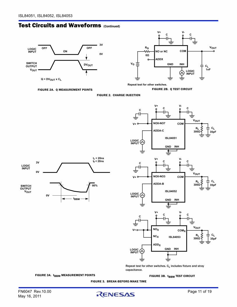
Test Circuits and Waveforms
FIGURE 1A. INHIBIT tON / tOFF MEASUREMENT POINTS
Repeat test for other switches. CL includes fixture and stray capacitance.
FIGURE 1B. INHIBIT tON/ tOFF TEST CIRCUIT
FIGURE 1. SWITCHING TIMES
50%
tr < 20nstf < 20ns
tON
3V
0V
tOFF
LOGICINPUT
SWITCHOUTPUT
90%
0V
90%VOUT
Logic input waveform is inverted for switches that have the oppositelogic sense.
VOUT V(NO or NC)
RLRL rON+----------------------=
LOGICINPUT
VOUT
RL
COM
NO0
INH
300Ω 35pF
GND
V-C
NO1-NO7
CL
V+
ADDA-C
C
LOGICINPUT
VOUT
RL
COMX
NCX
INH
300Ω 35pF
GND
NOX
CL
V+
ADDX
C
ISL84051
ISL84053
V+C
V-C
V+C
LOGICINPUT
VOUT
RL
COM
NO0
INH
300Ω 35pF
GND
V-C
NO1-NO3
CL
V+
ADDA-B
C
ISL84052
V+C
FN6047 Rev.10.00 Page 9 of 19May 16, 2011

ISL84051, ISL84052, ISL84053
FIGURE 1C. ADDRESS tTRANS MEASUREMENT POINTS
Repeat test for other switches. CL includes fixture and stray capacitance.
FIGURE 1D. ADDRESS tTRANS TEST CIRCUIT
FIGURE 1. SWITCHING TIMES (Continued)
Test Circuits and Waveforms (Continued)
50%
tr < 20nstf < 20ns
tTRANS
90%
3V
VNOX
0V
tTRANS
LOGICINPUT
SWITCHOUTPUT
10%
VOUT
0V
VNOX
Logic input waveform is inverted for switches that have the oppositelogic sense.
VOUT V(NO or NC)
RLRL rON+----------------------=
LOGICINPUT
VOUT
RL
COM
NO0
ADDA-C
300Ω 35pF
GND
NO1-NO6
CL
V+
INH
C
LOGICINPUT
VOUT
RL
COMX
NCX
ADDX
300Ω 35pF
GND
NOX
CL
V+
INH
C
ISL84051
ISL84053
V-C
V+C
V-C
V+C
NO7V-C
LOGICINPUT
VOUT
RL
COM
NO0
ADDA-B
300Ω 35pF
GND
NO1-NO2
CL
V+
INH
C
ISL84052
V-C
V+C
NO3V-C
V-C
FN6047 Rev.10.00 Page 10 of 19May 16, 2011
ISL84051, ISL84052, ISL84053
FIGURE 2A. Q MEASUREMENT POINTS FIGURE 2B. Q TEST CIRCUIT
FIGURE 2. CHARGE INJECTION
FIGURE 3A. tBBM MEASUREMENT POINTS
Repeat test for other switches. CL includes fixture and stray capacitance.
FIGURE 3B. tBBM TEST CIRCUIT
FIGURE 3. BREAK-BEFORE-MAKE TIME
Test Circuits and Waveforms (Continued)
VOUT
DVOUT
OFFON
OFF
Q = DVOUT x CL
SWITCHOUTPUT
LOGICINPUT
3V
0V
CL
VOUTRG
VG GND
COMNO or NC
LOGICINPUT
INH
ADDX
V-C
V+C
Repeat test for other switches.
1nF
0Ω
80%
3V
0V
tBBM
LOGICINPUT
SWITCHOUTPUT
0V
VOUT
tr < 20nstf < 20ns
LOGICINPUT
ADDA-C
COM
RL CL
VOUT
35pF300Ω
NO0-NO7
GND
V+
C
INH
LOGICINPUT
ADDX
COMX
RL CL
VOUT
35pF300Ω
NOX
NCX
GND
V+
INH
C
ISL84051
ISL84053
V-C
V+C
V-C
V+C
LOGICINPUT
ADDA-B
COM
RL CL
VOUT
35pF300Ω
NO0-NO3
GND
V+
C
INH
ISL84052
V-C
V+C
FN6047 Rev.10.00 Page 11 of 19May 16, 2011

ISL84051, ISL84052, ISL84053
Detailed DescriptionThe ISL84051, ISL84052, ISL84053 analog switches offer precise switching capability from a bipolar ±2V to ±6V or a single 2V to 12V supply with low on-resistance (60Ω) and high speed operation (tON = 50ns, tOFF = 40ns). The devices are especially well suited to portable battery powered equipment thanks to the low operating supply voltage (2V), low power consumption (3µW), low leakage currents (5nA max). High frequency applications also benefit from the wide bandwidth, and the very high off isolation and crosstalk rejection.
Supply Sequencing And Overvoltage ProtectionWith any CMOS device, proper power supply sequencing is required to protect the device from excessive input currents
which might permanently damage the IC. All I/O pins contain ESD protection diodes from the pin to V+ and to V- (see Figure 8). To prevent forward biasing these diodes, V+ and V- must be applied before any input signals, and input signal voltages must remain between V+ and V-. If these conditions cannot be guaranteed, then one of the following two protection methods should be employed.
Logic inputs can easily be protected by adding a 1kΩ resistor in series with the input (see Figure 8). The resistor limits the input current below the threshold that produces permanent damage, and the sub-microamp input current produces an insignificant voltage drop during normal operation.
This method is not applicable for the signal path inputs. Adding a series resistor to the switch input defeats the purpose of using a low rON switch, so two small signal diodes can be
FIGURE 4. OFF ISOLATION TEST CIRCUIT FIGURE 5. rON TEST CIRCUIT
FIGURE 6. CROSSTALK TEST CIRCUIT FIGURE 7. CAPACITANCE TEST CIRCUIT
Test Circuits and Waveforms (Continued)
ANALYZER
RL
SIGNALGENERATOR
0V OR V+
NO or NC
COM
ADDX
GND INH0V OR V+
V-C
V+C
0V OR V+
NO or NC
COM
ADDX
GND
VNX
V1
rON = V1/1mA
1mA
INH
V-C
V+C
0V OR V+
ANALYZER
NOA or NCA
SIGNALGENERATOR
RL
GND
ADDX
50Ω
NC
COMB
NOB or NCB
INH
ISL84052
V-C
V+C
COMA
ISL84053AND
GND
NO OR NC
COM
ADDXIMPEDANCEANALYZER
0V OR V+
INH
V-C
V+C
FN6047 Rev.10.00 Page 12 of 19May 16, 2011

ISL84051, ISL84052, ISL84053
added in series with the supply pins to provide overvoltage protection for all pins (see Figure 8). These additional diodes limit the analog signal from 1V below V+ to 1V above V-. The low leakage current performance is unaffected by this approach, but the switch resistance may increase, especially at low supply voltages.
Power-Supply ConsiderationsThe ISL8405x construction is typical of most CMOS analog switches, in that they have three supply pins: V+, V-, and GND. V+ and V- drive the internal CMOS switches and set their analog voltage limits, so there are no connections between the analog signal path and GND. Unlike switches with a 13V maximum supply voltage, the ISL8405x 15V maximum supply voltage provides plenty of room for the 10% tolerance of 12V supplies (±6V or 12V single supply), as well as room for overshoot and noise spikes.
This family of switches performs equally well when operated with bipolar or single voltage supplies. The minimum recommended supply voltage is 2V or ±2V. It is important to note that the input signal range, switching times, and ON-resistance degrade at lower supply voltages. Refer to the “Electrical Specification” tables beginning on page 5 and “Typical Performance Curves” beginning on page 14 for details.
V+ and GND power the internal logic (thus setting the digital switching point) and level shifters. The level shifters convert the logic levels to switched V+ and V- signals to drive the analog switch gate terminals.
Logic-Level ThresholdsV+ and GND power the internal logic stages, so V- has no affect on logic thresholds. This switch family is TTL compatible (0.8V and 2.4V) over a V+ supply range of 2.7V to 10V. At 12V the VIH level is about 3.5V. This is still below the CMOS guaranteed high output minimum level of 4V, but noise margin is reduced. For best results with a 12V supply, use a logic family that provides a VOH greater than 4V.
The digital input stages draw supply current whenever the digital input voltage is not at one of the supply rails. Driving the digital input signals from GND to V+ with a fast transition time minimizes power dissipation.
High-Frequency PerformanceIn 50Ω systems, signal response is reasonably flat even past 100MHz (see Figure 17). Figure 17 also illustrates that the frequency response is very consistent over varying analog signal levels.
An OFF switch acts like a capacitor and passes higher frequencies with less attenuation, resulting in signal feed through from a switch’s input to its output. Off isolation is the resistance to this feed through, while crosstalk indicates the amount of feed through from one switch to another. Figure 18 details the high off isolation and crosstalk rejection provided by this family. At 10MHz, off isolation is about 55dB in 50Ω systems, decreasing approximately 20dB per decade as frequency increases. Higher load impedances decrease off isolation and crosstalk rejection due to the voltage divider action of the switch OFF impedance and the load impedance.
Leakage ConsiderationsReverse ESD protection diodes are internally connected between each analog-signal pin and both V+ and V-. One of these diodes conducts if any analog signal exceeds V+ or V-.
Virtually all the analog leakage current comes from the ESD diodes to V+ or V-. Although the ESD diodes on a given signal pin are identical and therefore fairly well balanced, they are reverse biased differently. Each is biased by either V+ or V- and the analog signal. This means their leakages will vary as the signal varies. The difference in the two diode leakages to the V+ and V- pins constitutes the analog-signal-path leakage current. All analog leakage current flows between each pin and one of the supply terminals, not to the other switch terminal. This is why both sides of a given switch can show leakage currents of the same or opposite polarity. There is no connection between the analog signal paths and GND.
FIGURE 8. INPUT OVERVOLTAGE PROTECTION
V-
VCOMVNO OR NC
OPTIONAL PROTECTION
V+
LOGIC
DIODE
OPTIONAL PROTECTIONDIODE
OPTIONAL PROTECTIONRESISTORFOR LOGICINPUTS
1kΩ
FN6047 Rev.10.00 Page 13 of 19May 16, 2011

ISL84051, ISL84052, ISL84053
Typical Performance Curves TA = +25°C, Unless Otherwise Specified
FIGURE 9. ON-RESISTANCE vs SUPPLY VOLTAGE FIGURE 10. ON-RESISTANCE vs SWITCH VOLTAGE
FIGURE 11. ON-RESISTANCE vs SWITCH VOLTAGE FIGURE 12. CHARGE INJECTION vs SWITCH VOLTAGE
FIGURE 13. INHIBIT TURN-ON TIME vs SUPPLY VOLTAGE FIGURE 14. INHIBIT TURN-OFF TIME vs SUPPLY VOLTAGE
30
40
50
60
70
100
200
300
400
-40°C
+85°C
V- = 0V
r ON
(Ω
)
V+ (V)4 6 8 10 123 5 7 9 112
0
20
VCOM = (V+) - 1VICOM = 1mA
V- = -5V
+25°C
-40°C
+85°C
+25°C
75
100
150
200
225
6080
100120140160
405060708090
100
r ON
(Ω
)
VCOM (V)0 2 41 3 5
V+ = 2.7V
V+ = 5V
+25°C
-40°C
+85°C
ICOM = 1mA
V- = 0V
+25°C
-40°C
+85°C
V- = 0V
+25°C
+85°C
-40°C
V- = 0V
V+ = 3.3V
175
125
20
30
40
50
60
30
40
50
60
70
80905060708090
100110120
r ON
(Ω
)
VCOM (V)-4 -2 0 2 4-5 -3 -1 1 3 5
VS = ±5V
ICOM = 1mA VS = ±2V
+25°C+85°C
+25°C
-40°C
+85°C
-40°C
+25°C
-40°C
+85°C
VS = ±3V
-3
-2
-1
0
1
2
Q (
pC
)
VCOM (V)
-5 0 5-2.5 2.5
VS = ±5V
V+ = 5VV- = 0V
0
100
200
300
400
500
0
50
100
150
200
250
t ON
(n
s)
V+ (V)
2 4 6 8 10 123 5 7 9 11
-40°C
+85°C
V- = 0V
V- = -5V VCOM = (V+) - 1V
-40°C
+85°C
-40°C
+25°C
+25°C
+25°C
0
50
100
150
200
0
20
40
60
80
100
t OF
F (
ns
)
V+ (V)
2 4 6 8 10 123 5 7 9 11
-40°C
+85°C
VCOM = (V+) - 1V
V- = 0V
V- = -5V
-40°C+85°C
-40°C
+25°C
+25°C
+25°C
+85°C
FN6047 Rev.10.00 Page 14 of 19May 16, 2011

ISL84051, ISL84052, ISL84053
Die CharacteristicsSUBSTRATE POTENTIAL (POWERED UP):
V-
TRANSISTOR COUNT:ISL84051: 193ISL84052: 193ISL84053: 193
PROCESS:Si Gate CMOS
FIGURE 15. ADDRESS TRANS TIME vs SINGLE SUPPLY VOLTAGE FIGURE 16. ADDRESS TRANS TIME vs DUAL SUPPLY VOLTAGE
FIGURE 17. FREQUENCY RESPONSE FIGURE 18. CROSSTALK AND OFF ISOLATION
Typical Performance Curves TA = +25°C, Unless Otherwise Specified (Continued)
2 4 6 8 10 123 5 7 9 11 13
V+ (V)
+85°C
V- = 0V
VCOM = (V+) - 1V
-40°C
0
50
100
150
200
250
300
t RA
NS
(n
s)
+25°C
V± (V)
2 3 4 5 6
VCOM = (V+) - 1V
t RA
NS
(n
s)
50
100
150
200
250
+85°C
-40°C
+25°C
0
FREQUENCY (Hz)
3
0
-3
NO
RM
AL
IZE
D G
AIN
(d
B)
0
45
90
135
180
PH
AS
E (
°)
1M 10M 100M 600M
VIN = 0.2VP-P TO 5VP-P
GAIN
PHASE
VS = ±5V
RL = 50Ω
ISL84053
ISL84051
ISL84051
ISL84053
ISL84052
ISL84052
FREQUENCY (Hz)
1k 100k 1M 100M 500M10k 10M-110
-10
-20
-30
-40
-50
-60
-70
-80
-90
-100
CR
OS
STA
LK
(d
B)
OF
F I
SO
LA
TIO
N (
dB
)
110
10
20
30
40
50
60
70
80
90
100
ISOLATION
CROSSTALK
RL = 50Ω
VS = ±2V TO ±5VV+ = 3V TO 12V or
FN6047 Rev.10.00 Page 15 of 19May 16, 2011
ISL84051, ISL84052, ISL84053
ProductsIntersil Corporation is a leader in the design and manufacture of high-performance analog semiconductors. The Company's products address some of the industry's fastest growing markets, such as, flat panel displays, cell phones, handheld products, and notebooks. Intersil's product families address power management and analog signal processing functions. Go to www.intersil.com/products for a complete list of Intersil product families.
*For a complete listing of Applications, Related Documentation and Related Parts, please see the respective device information page on intersil.com: ISL84051, ISL84052, ISL84053
To report errors or suggestions for this datasheet, please go to: www.intersil.com/askourstaff
FITs are available from our website at: http://rel.intersil.com/reports/search.php
Revision HistoryThe revision history provided is for informational purposes only and is believed to be accurate, but not warranted. Please go to web to make sure you have the latest revision.
DATE REVISION CHANGE
05/02/11 FN6047.10 -Converted to new datasheet template.
-Updated Intersil Trademark statement at bottom of page 1 per directive from Legal.
-Added TSSOP Package option to ISL84053 in Pin Configuration and ordering information.
-Updated ordering information by removing withdrawn and obsolete non pb-free parts: ISL84051IA, ISL84051IA-T, ISL84051IB, ISL84051IB-T, ISL84052IA, ISL84051IB, ISL84053IA-TUpdated notes in ordering information
-Updated “Parameters...” note in Electrical Specifications tables to new “Compliance...” note according to standards
-M16.173 - Converted to new POD format by moving dimensions from table onto drawing and adding land pattern. No dimension changes.
-Added Revision History and Products Information.
FN6047 Rev.10.00 Page 16 of 19May 16, 2011
ISL84051, ISL84052, ISL84053
FN6047 Rev.10.00 Page 17 of 19May 16, 2011
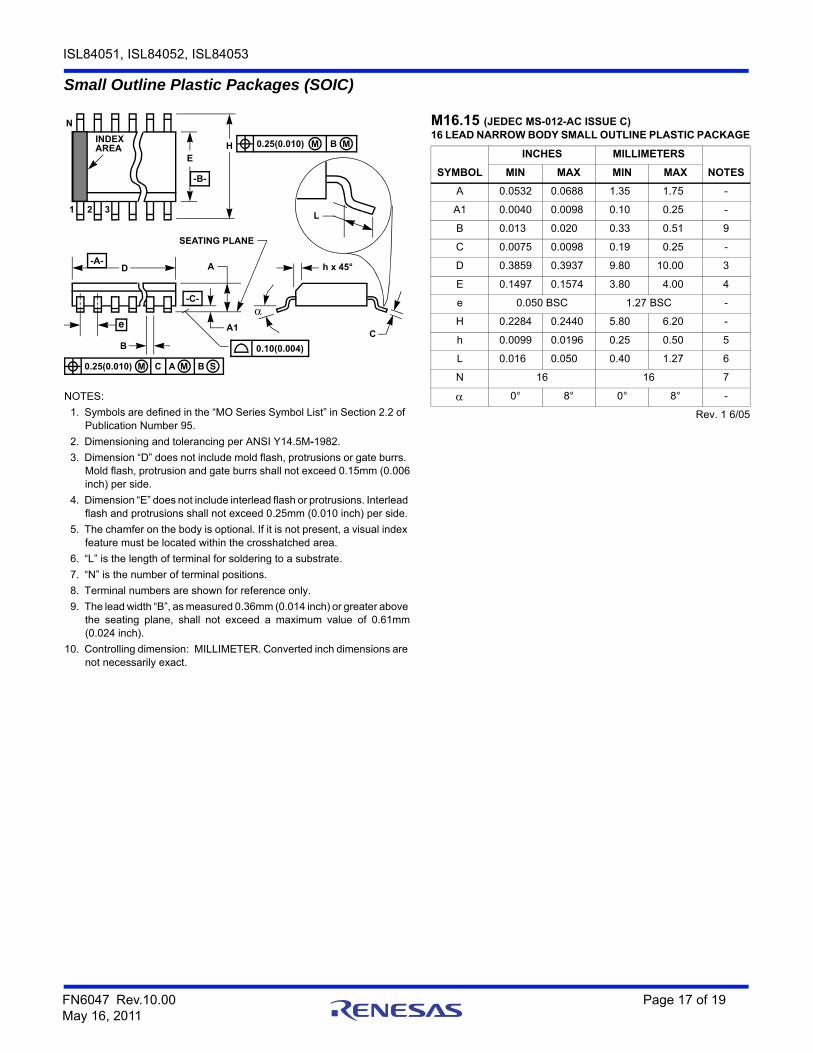
Small Outline Plastic Packages (SOIC)
NOTES:
1. Symbols are defined in the “MO Series Symbol List” in Section 2.2 of Publication Number 95.
2. Dimensioning and tolerancing per ANSI Y14.5M-1982.
3. Dimension “D” does not include mold flash, protrusions or gate burrs. Mold flash, protrusion and gate burrs shall not exceed 0.15mm (0.006inch) per side.
4. Dimension “E” does not include interlead flash or protrusions. Interlead flash and protrusions shall not exceed 0.25mm (0.010 inch) per side.
5. The chamfer on the body is optional. If it is not present, a visual index feature must be located within the crosshatched area.
6. “L” is the length of terminal for soldering to a substrate.
7. “N” is the number of terminal positions.
8. Terminal numbers are shown for reference only.
9. The lead width “B”, as measured 0.36mm (0.014 inch) or greater above the seating plane, shall not exceed a maximum value of 0.61mm(0.024 inch).
10. Controlling dimension: MILLIMETER. Converted inch dimensions are not necessarily exact.
INDEXAREA
E
D
N
1 2 3
-B-
0.25(0.010) C AM B S
e
-A-
L
B
M
-C-
A1
A
SEATING PLANE
0.10(0.004)
h x 45°
C
H 0.25(0.010) BM M
M16.15 (JEDEC MS-012-AC ISSUE C)16 LEAD NARROW BODY SMALL OUTLINE PLASTIC PACKAGE
SYMBOL
INCHES MILLIMETERS
NOTESMIN MAX MIN MAX
A 0.0532 0.0688 1.35 1.75 -
A1 0.0040 0.0098 0.10 0.25 -
B 0.013 0.020 0.33 0.51 9
C 0.0075 0.0098 0.19 0.25 -
D 0.3859 0.3937 9.80 10.00 3
E 0.1497 0.1574 3.80 4.00 4
e 0.050 BSC 1.27 BSC -
H 0.2284 0.2440 5.80 6.20 -
h 0.0099 0.0196 0.25 0.50 5
L 0.016 0.050 0.40 1.27 6
N 16 16 7
0° 8° 0° 8° -
Rev. 1 6/05
ISL84051, ISL84052, ISL84053
FN6047 Rev.10.00 Page 18 of 19May 16, 2011
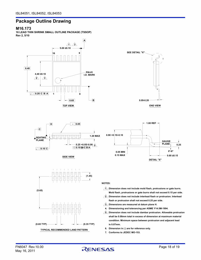
Package Outline Drawing
M16.17316 LEAD THIN SHRINK SMALL OUTLINE PACKAGE (TSSOP)Rev 2, 5/10
0.09-0.20
SEE DETAIL "X"
DETAIL "X"
TYPICAL RECOMMENDED LAND PATTERN
TOP VIEW
SIDE VIEW
END VIEW
Dimension does not include mold flash, protrusions or gate burrs.
Mold flash, protrusions or gate burrs shall not exceed 0.15 per side.
Dimension does not include interlead flash or protrusion. Interlead
flash or protrusion shall not exceed 0.25 per side.
Dimensions are measured at datum plane H.
Dimensioning and tolerancing per ASME Y14.5M-1994.
Dimension does not include dambar protrusion. Allowable protrusion
shall be 0.08mm total in excess of dimension at maximum material
condition. Minimum space between protrusion and adjacent lead
is 0.07mm.
Dimension in ( ) are for reference only.
Conforms to JEDEC MO-153.
6.
3.
5.
4.
2.
1.
NOTES:
7.
(0.65 TYP)
(5.65)
(0.35 TYP)
0.90 +0.15/-0.10
0.60 ±0.150.15 MAX
0.05 MIN
PLANEGAUGE
0°-8°
0.25
1.00 REF
(1.45)
16
2
1
3
8
B
1 3
9
A
PIN #1I.D. MARK
5.00 ±0.10
6.40
4.40 ±0.10
0.65
1.20 MAX
SEATINGPLANE
0.25 +0.05/-0.06 5
C
H
0.20 C B A
0.10 C
- 0.05
0.10 C B AM

FN6047 Rev.10.00 Page 19 of 19May 16, 2011
ISL84051, ISL84052, ISL84053
Intersil products are manufactured, assembled and tested utilizing ISO9001 quality systems as notedin the quality certifications found at www.intersil.com/en/support/qualandreliability.html
Intersil products are sold by description only. Intersil may modify the circuit design and/or specifications of products at any time without notice, provided that such modification does not, in Intersil's sole judgment, affect the form, fit or function of the product. Accordingly, the reader is cautioned to verify that datasheets are current before placing orders. Information furnished by Intersil is believed to be accurate and reliable. However, no responsibility is assumed by Intersil or its subsidiaries for its use; nor for any infringements of patents or other rights of third parties which may result from its use. No license is granted by implication or otherwise under any patent or patent rights of Intersil or its subsidiaries.
For information regarding Intersil Corporation and its products, see www.intersil.com
For additional products, see www.intersil.com/en/products.html
© Copyright Intersil Americas LLC 2003-2011. All Rights Reserved.All trademarks and registered trademarks are the property of their respective owners.
Shrink Small Outline Plastic Packages (SSOP)Quarter Size Outline Plastic Packages (QSOP)
NOTES:
1. Symbols are defined in the “MO Series Symbol List” in Section 2.2 of Publication Number 95.
2. Dimensioning and tolerancing per ANSI Y14.5M-1982.
3. Dimension “D” does not include mold flash, protrusions or gate burrs. Mold flash, protrusion and gate burrs shall not exceed0.15mm (0.006 inch) per side.
4. Dimension “E” does not include interlead flash or protrusions. Interlead flash and protrusions shall not exceed 0.25mm (0.010inch) per side.
5. The chamfer on the body is optional. If it is not present, a visual index feature must be located within the crosshatched area.
6. “L” is the length of terminal for soldering to a substrate.
7. “N” is the number of terminal positions.
8. Terminal numbers are shown for reference only.
9. Dimension “B” does not include dambar protrusion. Allowable dambar protrusion shall be 0.10mm (0.004 inch) total in excessof “B” dimension at maximum material condition.
10. Controlling dimension: INCHES. Converted millimeter dimen-sions are not necessarily exact.
INDEXAREA
E
D
N
1 2 3
-B-
0.17(0.007) C AM B S
e
-A-
B
M
-C-
A1
A
SEATING PLANE
0.10(0.004)
h x 45°
C
H 0.25(0.010) BM M
L0.25
0.010
GAUGEPLANE
A2
M16.15A16 LEAD SHRINK SMALL OUTLINE PLASTIC PACKAGE (0.150” WIDE BODY)
SYMBOL
INCHES MILLIMETERS
NOTESMIN MAX MIN MAX
A 0.061 0.068 1.55 1.73 -
A1 0.004 0.0098 0.102 0.249 -
A2 0.055 0.061 1.40 1.55 -
B 0.008 0.012 0.20 0.31 9
C 0.0075 0.0098 0.191 0.249 -
D 0.189 0.196 4.80 4.98 3
E 0.150 0.157 3.81 3.99 4
e 0.025 BSC 0.635 BSC -
H 0.230 0.244 5.84 6.20 -
h 0.010 0.016 0.25 0.41 5
L 0.016 0.035 0.41 0.89 6
N 16 16 7
0° 8° 0° 8° -
Rev. 2 6/04