74HC4052; 74HCT4052 Dual 4-channel analog multiplexer ... · PDF file2004 Nov 11 3 Philips...
27
DATA SHEET Product specification Supersedes data of 2003 May 16 2004 Nov 11 INTEGRATED CIRCUITS 74HC4052; 74HCT4052 Dual 4-channel analog multiplexer, demultiplexer
Transcript of 74HC4052; 74HCT4052 Dual 4-channel analog multiplexer ... · PDF file2004 Nov 11 3 Philips...
DATA SHEET
Product specificationSupersedes data of 2003 May 16
2004 Nov 11
INTEGRATED CIRCUITS
74HC4052; 74HCT4052Dual 4-channel analog multiplexer,demultiplexer
Philips Semiconductors Product specification
Dual 4-channel analog multiplexer,demultiplexer
74HC4052; 74HCT4052
FEATURES
• Wide analog input voltage range from −5 V to +5 V
• Low ON-resistance:
– 80 Ω (typical) at VCC − VEE = 4.5 V
– 70 Ω (typical) at VCC − VEE = 6.0 V
– 60 Ω (typical) at VCC − VEE = 9.0 V
• Logic level translation: to enable 5 V logic tocommunicate with ±5 V analog signals
• Typical “break before make” built in
• Complies with JEDEC standard no. 7A
• ESD protection:
– HBM EIA/JESD22-A114-B exceeds 2000 V
– MM EIA/JESD22-A115-A exceeds 200 V.
• Specified from −40 °C to +85 °C and −40 °C to +125 °C.
APPLICATIONS
• Analog multiplexing and demultiplexing
• Digital multiplexing and demultiplexing
• Signal gating.
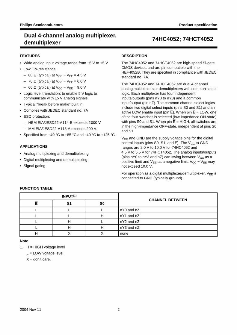
DESCRIPTION
The 74HC4052 and 74HCT4052 are high-speed Si-gateCMOS devices and are pin compatible with theHEF4052B. They are specified in compliance with JEDECstandard no. 7A.
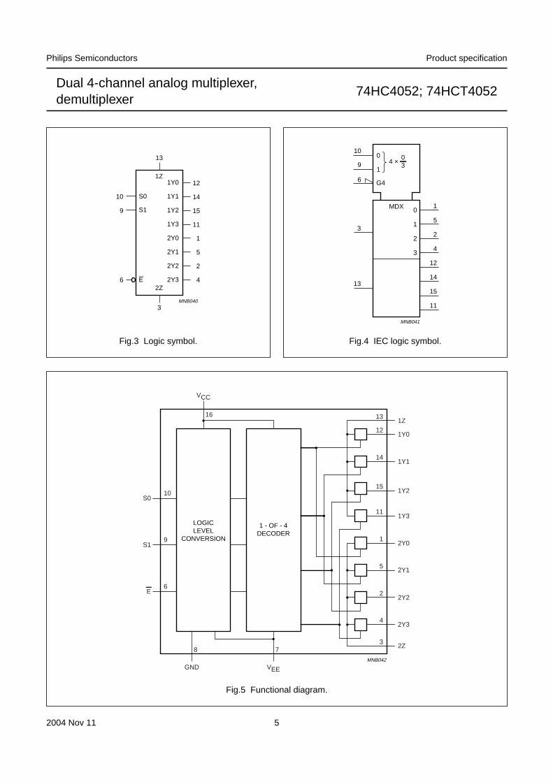
The 74HC4052 and 74HCT4052 are dual 4-channelanalog multiplexers or demultiplexers with common selectlogic. Each multiplexer has four independentinputs/outputs (pins nY0 to nY3) and a commoninput/output (pin nZ). The common channel select logicsinclude two digital select inputs (pins S0 and S1) and anactive LOW enable input (pin E). When pin E = LOW, oneof the four switches is selected (low-impedance ON-state)with pins S0 and S1. When pin E = HIGH, all switches arein the high-impedance OFF-state, independent of pins S0and S1.
VCC and GND are the supply voltage pins for the digitalcontrol inputs (pins S0, S1, and E). The VCC to GNDranges are 2.0 V to 10.0 V for 74HC4052 and4.5 V to 5.5 V for 74HCT4052. The analog inputs/outputs(pins nY0 to nY3 and nZ) can swing between VCC as apositive limit and VEE as a negative limit. VCC − VEE maynot exceed 10.0 V.
For operation as a digital multiplexer/demultiplexer, VEE isconnected to GND (typically ground).
FUNCTION TABLE
Note
1. H = HIGH voltage level
L = LOW voltage level
X = don’t care.
INPUT(1)
CHANNEL BETWEENE S1 S0
L L L nY0 and nZ
L L H nY1 and nZ
L H L nY2 and nZ
L H H nY3 and nZ
H X X none
2004 Nov 11 2
Philips Semiconductors Product specification
Dual 4-channel analog multiplexer,demultiplexer
74HC4052; 74HCT4052
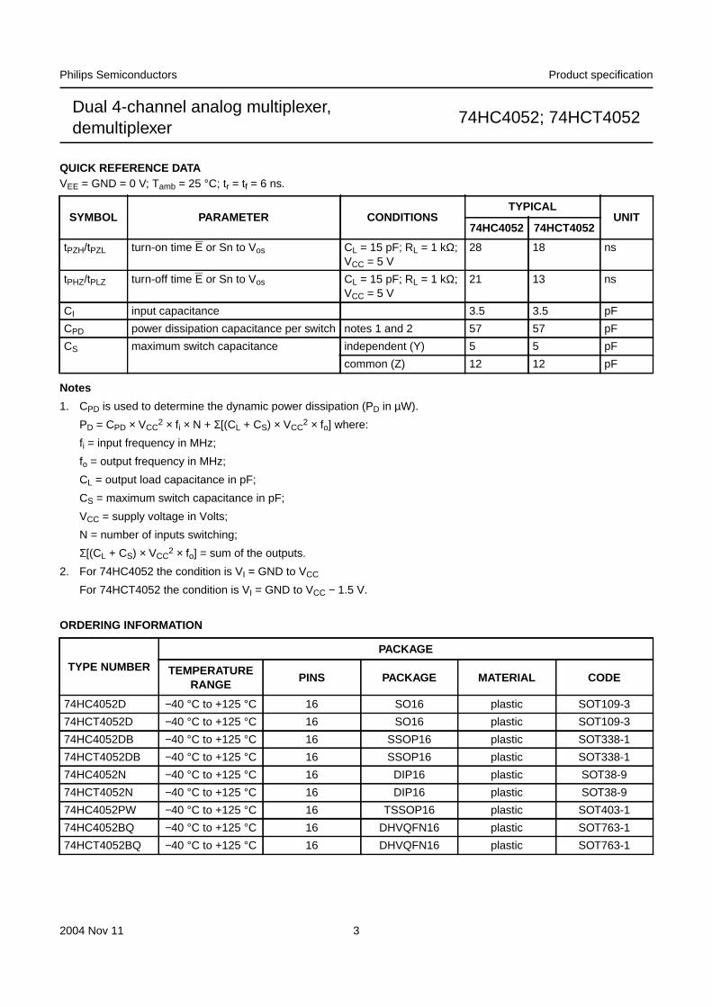
QUICK REFERENCE DATAVEE = GND = 0 V; Tamb = 25 °C; tr = tf = 6 ns.
Notes
1. CPD is used to determine the dynamic power dissipation (PD in µW).
PD = CPD × VCC2 × fi × N + Σ[(CL + CS) × VCC
2 × fo] where:
fi = input frequency in MHz;
fo = output frequency in MHz;
CL = output load capacitance in pF;
CS = maximum switch capacitance in pF;
VCC = supply voltage in Volts;
N = number of inputs switching;
Σ[(CL + CS) × VCC2 × fo] = sum of the outputs.
2. For 74HC4052 the condition is VI = GND to VCC
For 74HCT4052 the condition is VI = GND to VCC − 1.5 V.
ORDERING INFORMATION
SYMBOL PARAMETER CONDITIONSTYPICAL
UNIT74HC4052 74HCT4052
tPZH/tPZL turn-on time E or Sn to Vos CL = 15 pF; RL = 1 kΩ;VCC = 5 V
28 18 ns
tPHZ/tPLZ turn-off time E or Sn to Vos CL = 15 pF; RL = 1 kΩ;VCC = 5 V
21 13 ns
CI input capacitance 3.5 3.5 pF
CPD power dissipation capacitance per switch notes 1 and 2 57 57 pF
CS maximum switch capacitance independent (Y) 5 5 pF
common (Z) 12 12 pF
TYPE NUMBER
PACKAGE
TEMPERATURERANGE
PINS PACKAGE MATERIAL CODE
74HC4052D −40 °C to +125 °C 16 SO16 plastic SOT109-3
74HCT4052D −40 °C to +125 °C 16 SO16 plastic SOT109-3
74HC4052DB −40 °C to +125 °C 16 SSOP16 plastic SOT338-1
74HCT4052DB −40 °C to +125 °C 16 SSOP16 plastic SOT338-1
74HC4052N −40 °C to +125 °C 16 DIP16 plastic SOT38-9
74HCT4052N −40 °C to +125 °C 16 DIP16 plastic SOT38-9
74HC4052PW −40 °C to +125 °C 16 TSSOP16 plastic SOT403-1
74HC4052BQ −40 °C to +125 °C 16 DHVQFN16 plastic SOT763-1
74HCT4052BQ −40 °C to +125 °C 16 DHVQFN16 plastic SOT763-1
2004 Nov 11 3
Philips Semiconductors Product specification
Dual 4-channel analog multiplexer,demultiplexer
74HC4052; 74HCT4052
PINNING
PIN SYMBOL DESCRIPTION
1 2Y0 independent input or output
2 2Y2 independent input or output
3 2Z common input or output
4 2Y3 independent input or output
5 2Y1 independent input or output
6 E enable input (active LOW)
7 VEE negative supply voltage
8 GND ground (0 V)
9 S1 select logic input
10 S0 select logic input
11 1Y3 independent input or output
12 1Y0 independent input or output
13 1Z common input or output
14 1Y1 independent input or output
15 1Y2 independent input or output
16 VCC positive supply voltage
handbook, halfpage
4052
MNB039
1
2
3
4
5
6
7
8
16
15
14
13
12
11
10
9
2Y0
2Y2
2Z
2Y3
2Y1
E
VEE
GND S1
S0
1Y3
1Y0
1Z
1Y1
1Y2
VCC
Fig.1 Pin configuration DIP16, SO16 and(T)SSOP16. Fig.2 Pin configuration DHVQFN16.
(1) The die substrate is attached to this pad using conductive dieattach material. It can not be used as a supply pin or input.
001aac117
4052
VCC(1)
VEE S0
E 1Y3
2Y1 1Y0
2Y3 1Z
2Z 1Y1
2Y2 1Y2
GN
D S1
2Y0
VC
C
Transparent top view
7 10
6 11
5 12
4 13
3 14
2 15
8 9
1 16
terminal 1index area
2004 Nov 11 4
Philips Semiconductors Product specification
Dual 4-channel analog multiplexer,demultiplexer
74HC4052; 74HCT4052
handbook, halfpage
MNB040
4
2
5
1
11
15
14
12
13
3
6
9
1Z
S0
S1
E2Z
2Y3
2Y2
2Y1
2Y0
1Y3
1Y2
1Y1
1Y0
10
Fig.3 Logic symbol.
handbook, halfpage
MNB041
11
15
14
12
4
2
5
91
100
6 G4
MDX
03
4 ×
1
3
2
1
0
13
3
Fig.4 IEC logic symbol.
handbook, full pagewidth
MNB042
1 - OF - 4DECODER
LOGICLEVEL
CONVERSION
78
VEEGND
VCC
12
1316
3
14
15
11
10
9
6
S0
S1
E
1
5
2
1Y0
1Z
2Z
1Y1
1Y2
1Y3
2Y0
2Y1
2Y2
2Y34
Fig.5 Functional diagram.
2004 Nov 11 5
Philips Semiconductors Product specification
Dual 4-channel analog multiplexer,demultiplexer
74HC4052; 74HCT4052
handbook, full pagewidth
MNB043
fromlogic
VCC
VEE
VEE
VCC
VCC
VEE
nYn
nZ
VCC
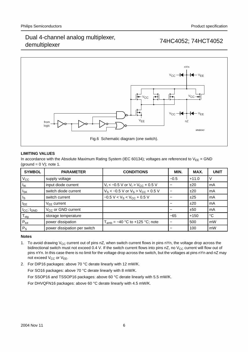
Fig.6 Schematic diagram (one switch).
LIMITING VALUESIn accordance with the Absolute Maximum Rating System (IEC 60134); voltages are referenced to VEE = GND(ground = 0 V); note 1.
Notes
1. To avoid drawing VCC current out of pins nZ, when switch current flows in pins nYn, the voltage drop across thebidirectional switch must not exceed 0.4 V. If the switch current flows into pins nZ, no VCC current will flow out ofpins nYn. In this case there is no limit for the voltage drop across the switch, but the voltages at pins nYn and nZ maynot exceed VCC or VEE.
2. For DIP16 packages: above 70 °C derate linearly with 12 mW/K.
For SO16 packages: above 70 °C derate linearly with 8 mW/K.
For SSOP16 and TSSOP16 packages: above 60 °C derate linearly with 5.5 mW/K.
For DHVQFN16 packages: above 60 °C derate linearly with 4.5 mW/K.
SYMBOL PARAMETER CONDITIONS MIN. MAX. UNIT
VCC supply voltage −0.5 +11.0 V
IIK input diode current VI < −0.5 V or VI > VCC + 0.5 V − ±20 mA
ISK switch diode current VS < −0.5 V or VS > VCC + 0.5 V − ±20 mA
IS switch current −0.5 V < VS < VCC + 0.5 V − ±25 mA
IEE VEE current − ±20 mA
ICC; IGND VCC or GND current − ±50 mA
Tstg storage temperature −65 +150 °CPtot power dissipation Tamb = −40 °C to +125 °C; note − 500 mW
PS power dissipation per switch − 100 mW
2004 Nov 11 6
Philips Semiconductors Product specification
Dual 4-channel analog multiplexer,demultiplexer
74HC4052; 74HCT4052
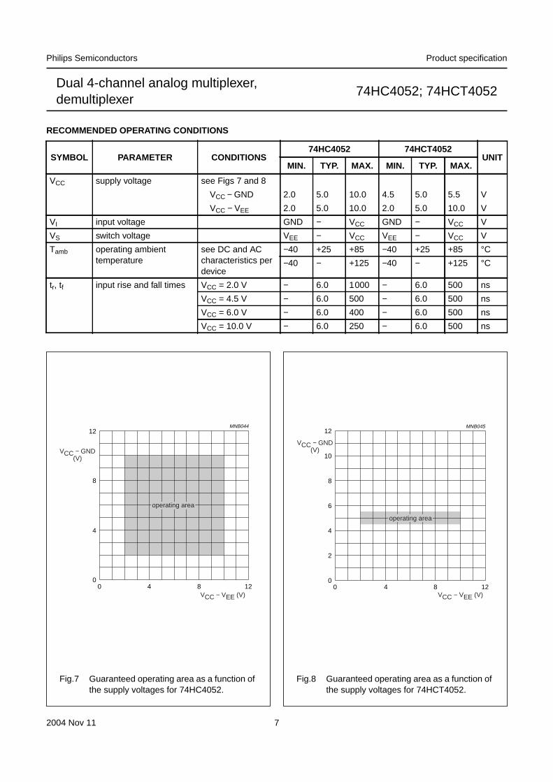
RECOMMENDED OPERATING CONDITIONS
SYMBOL PARAMETER CONDITIONS74HC4052 74HCT4052
UNITMIN. TYP. MAX. MIN. TYP. MAX.
VCC supply voltage see Figs 7 and 8
VCC − GND 2.0 5.0 10.0 4.5 5.0 5.5 V
VCC − VEE 2.0 5.0 10.0 2.0 5.0 10.0 V
VI input voltage GND − VCC GND − VCC V
VS switch voltage VEE − VCC VEE − VCC V
Tamb operating ambienttemperature
see DC and ACcharacteristics perdevice
−40 +25 +85 −40 +25 +85 °C−40 − +125 −40 − +125 °C
tr, tf input rise and fall times VCC = 2.0 V − 6.0 1000 − 6.0 500 ns
VCC = 4.5 V − 6.0 500 − 6.0 500 ns
VCC = 6.0 V − 6.0 400 − 6.0 500 ns
VCC = 10.0 V − 6.0 250 − 6.0 500 ns
handbook, halfpage
0 4 12
12
0
4
8
8
MNB044
operating area
VCC − GND(V)
VCC − VEE (V)
Fig.7 Guaranteed operating area as a function ofthe supply voltages for 74HC4052.
handbook, halfpage
0
12
6
10
8
2
4
0 4 128
MNB045
operating area
VCC − GND(V)
VCC − VEE (V)
Fig.8 Guaranteed operating area as a function ofthe supply voltages for 74HCT4052.
2004 Nov 11 7
Philips Semiconductors Product specification
Dual 4-channel analog multiplexer,demultiplexer
74HC4052; 74HCT4052
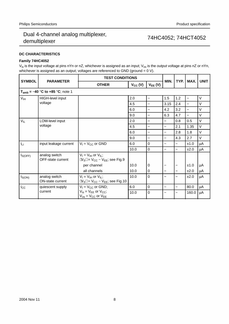
DC CHARACTERISTICS
Family 74HC4052Vis is the input voltage at pins nYn or nZ, whichever is assigned as an input; Vos is the output voltage at pins nZ or nYn,whichever is assigned as an output; voltages are referenced to GND (ground = 0 V).
SYMBOL PARAMETERTEST CONDITIONS
MIN. TYP. MAX. UNITOTHER VCC (V) VEE (V)
Tamb = −40 °C to +85 °C; note 1
VIH HIGH-level inputvoltage
2.0 − 1.5 1.2 − V
4.5 − 3.15 2.4 − V
6.0 − 4.2 3.2 − V
9.0 − 6.3 4.7 − V
VIL LOW-level inputvoltage
2.0 − − 0.8 0.5 V
4.5 − − 2.1 1.35 V
6.0 − − 2.8 1.8 V
9.0 − − 4.3 2.7 V
ILI input leakage current VI = VCC or GND 6.0 0 − − ±1.0 µA
10.0 0 − − ±2.0 µA
IS(OFF) analog switchOFF-state current
VI = VIH or VIL;VS = VCC − VEE; see Fig.9
per channel 10.0 0 − − ±1.0 µA
all channels 10.0 0 − − ±2.0 µA
IS(ON) analog switchON-state current
VI = VIH or VIL;VS = VCC − VEE; see Fig.10
10.0 0 − − ±2.0 µA
ICC quiescent supplycurrent
VI = VCC or GND;Vis = VEE or VCC;Vos = VCC or VEE
6.0 0 − − 80.0 µA
10.0 0 − − 160.0 µA
2004 Nov 11 8
Philips Semiconductors Product specification
Dual 4-channel analog multiplexer,demultiplexer
74HC4052; 74HCT4052
Note
1. All typical values are measured at Tamb = 25 °C.
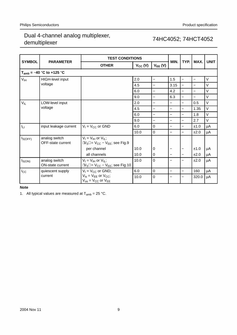
Tamb = −40 °C to +125 °C
VIH HIGH-level inputvoltage
2.0 − 1.5 − − V
4.5 − 3.15 − − V
6.0 − 4.2 − − V
9.0 − 6.3 − − V
VIL LOW-level inputvoltage
2.0 − − − 0.5 V
4.5 − − − 1.35 V
6.0 − − − 1.8 V
9.0 − − − 2.7 V
ILI input leakage current VI = VCC or GND 6.0 0 − − ±1.0 µA
10.0 0 − − ±2.0 µA
IS(OFF) analog switchOFF-state current
VI = VIH or VIL;VS = VCC − VEE; see Fig.9
per channel 10.0 0 − − ±1.0 µA
all channels 10.0 0 − − ±2.0 µA
IS(ON) analog switchON-state current
VI = VIH or VIL;VS = VCC − VEE; see Fig.10
10.0 0 − − ±2.0 µA
ICC quiescent supplycurrent
VI = VCC or GND;Vis = VEE or VCC;Vos = VCC or VEE
6.0 0 − − 160 µA
10.0 0 − − 320.0 µA
SYMBOL PARAMETERTEST CONDITIONS
MIN. TYP. MAX. UNITOTHER VCC (V) VEE (V)
2004 Nov 11 9
Philips Semiconductors Product specification
Dual 4-channel analog multiplexer,demultiplexer
74HC4052; 74HCT4052
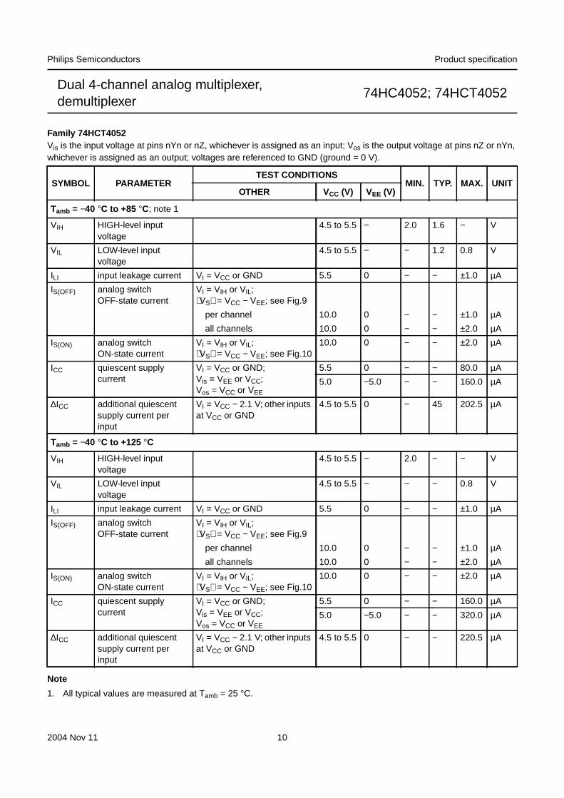
Family 74HCT4052Vis is the input voltage at pins nYn or nZ, whichever is assigned as an input; Vos is the output voltage at pins nZ or nYn,whichever is assigned as an output; voltages are referenced to GND (ground = 0 V).
Note
1. All typical values are measured at Tamb = 25 °C.
SYMBOL PARAMETERTEST CONDITIONS
MIN. TYP. MAX. UNITOTHER VCC (V) VEE (V)
Tamb = −40 °C to +85 °C; note 1
VIH HIGH-level inputvoltage
4.5 to 5.5 − 2.0 1.6 − V
VIL LOW-level inputvoltage
4.5 to 5.5 − − 1.2 0.8 V
ILI input leakage current VI = VCC or GND 5.5 0 − − ±1.0 µA
IS(OFF) analog switchOFF-state current
VI = VIH or VIL;VS = VCC − VEE; see Fig.9
per channel 10.0 0 − − ±1.0 µA
all channels 10.0 0 − − ±2.0 µA
IS(ON) analog switchON-state current
VI = VIH or VIL;VS = VCC − VEE; see Fig.10
10.0 0 − − ±2.0 µA
ICC quiescent supplycurrent
VI = VCC or GND;Vis = VEE or VCC;Vos = VCC or VEE
5.5 0 − − 80.0 µA
5.0 −5.0 − − 160.0 µA
∆ICC additional quiescentsupply current perinput
VI = VCC − 2.1 V; other inputsat VCC or GND
4.5 to 5.5 0 − 45 202.5 µA
Tamb = −40 °C to +125 °C
VIH HIGH-level inputvoltage
4.5 to 5.5 − 2.0 − − V
VIL LOW-level inputvoltage
4.5 to 5.5 − − − 0.8 V
ILI input leakage current VI = VCC or GND 5.5 0 − − ±1.0 µA
IS(OFF) analog switchOFF-state current
VI = VIH or VIL;VS = VCC − VEE; see Fig.9
per channel 10.0 0 − − ±1.0 µA
all channels 10.0 0 − − ±2.0 µA
IS(ON) analog switchON-state current
VI = VIH or VIL;VS = VCC − VEE; see Fig.10
10.0 0 − − ±2.0 µA
ICC quiescent supplycurrent
VI = VCC or GND;Vis = VEE or VCC;Vos = VCC or VEE
5.5 0 − − 160.0 µA
5.0 −5.0 − − 320.0 µA
∆ICC additional quiescentsupply current perinput
VI = VCC − 2.1 V; other inputsat VCC or GND
4.5 to 5.5 0 − − 220.5 µA
2004 Nov 11 10
Philips Semiconductors Product specification
Dual 4-channel analog multiplexer,demultiplexer
74HC4052; 74HCT4052
handbook, full pagewidth
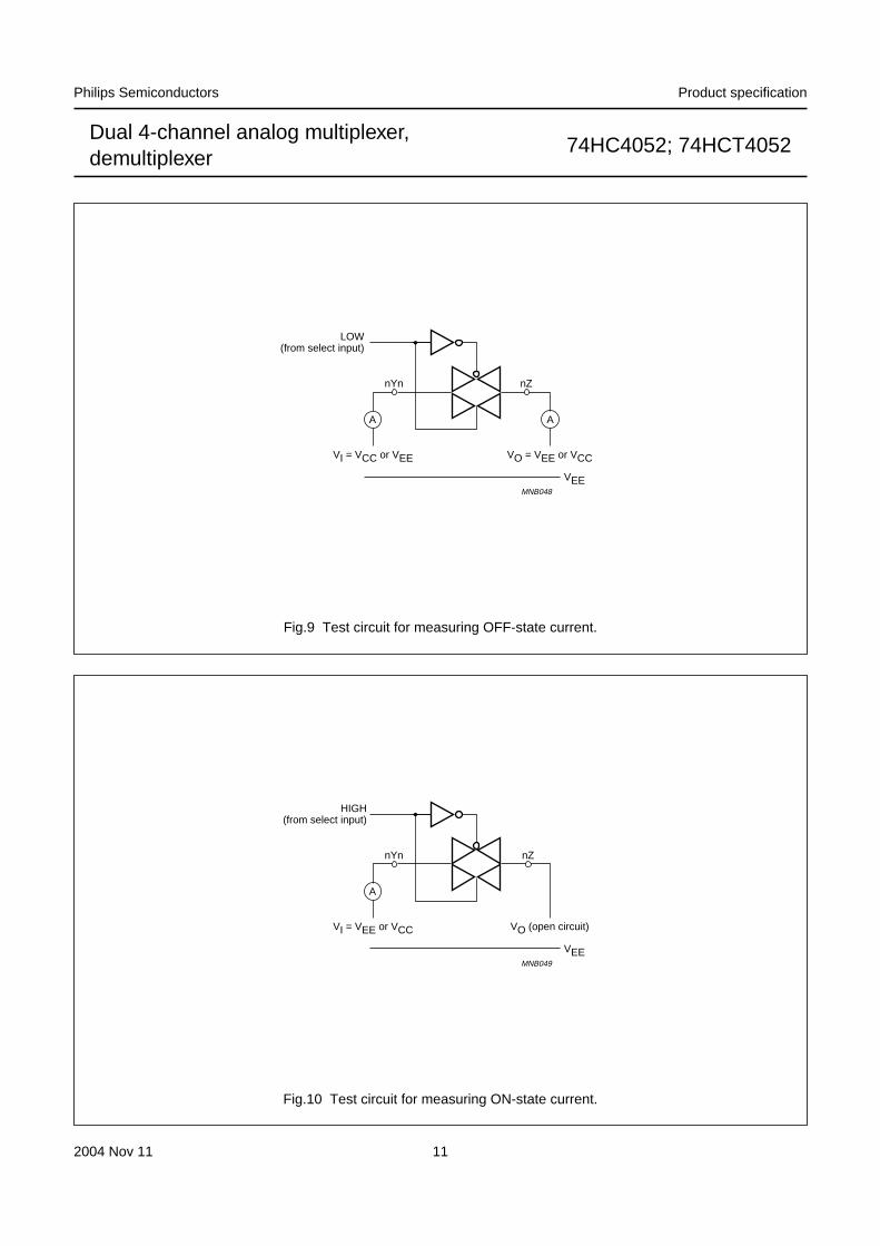
MNB048
A A
nYn nZ
VI = VCC or VEE VO = VEE or VCC
LOW(from select input)
VEE
Fig.9 Test circuit for measuring OFF-state current.
handbook, full pagewidth
MNB049
A
nYn nZ
VI = VEE or VCC VO (open circuit)
HIGH(from select input)
VEE
Fig.10 Test circuit for measuring ON-state current.
2004 Nov 11 11
Philips Semiconductors Product specification
Dual 4-channel analog multiplexer,demultiplexer
74HC4052; 74HCT4052
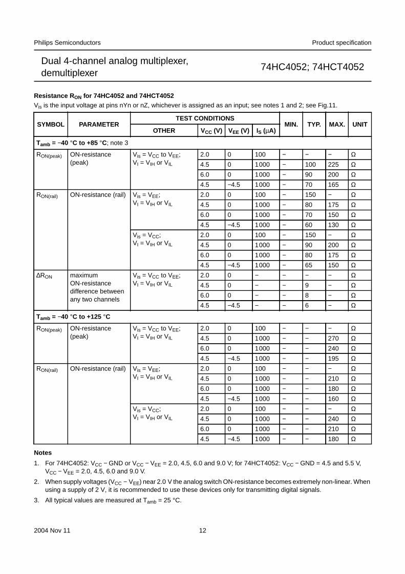
Resistance R ON for 74HC4052 and 74HCT4052Vis is the input voltage at pins nYn or nZ, whichever is assigned as an input; see notes 1 and 2; see Fig.11.
Notes
1. For 74HC4052: VCC − GND or VCC − VEE = 2.0, 4.5, 6.0 and 9.0 V; for 74HCT4052: VCC − GND = 4.5 and 5.5 V,VCC − VEE = 2.0, 4.5, 6.0 and 9.0 V.
2. When supply voltages (VCC − VEE) near 2.0 V the analog switch ON-resistance becomes extremely non-linear. Whenusing a supply of 2 V, it is recommended to use these devices only for transmitting digital signals.
3. All typical values are measured at Tamb = 25 °C.
SYMBOL PARAMETERTEST CONDITIONS
MIN. TYP. MAX. UNITOTHER VCC (V) VEE (V) IS (µA)
Tamb = −40 °C to +85 °C; note 3
RON(peak) ON-resistance(peak)
Vis = VCC to VEE;VI = VIH or VIL
2.0 0 100 − − − Ω4.5 0 1000 − 100 225 Ω6.0 0 1000 − 90 200 Ω4.5 −4.5 1000 − 70 165 Ω
RON(rail) ON-resistance (rail) Vis = VEE;VI = VIH or VIL
2.0 0 100 − 150 − Ω4.5 0 1000 − 80 175 Ω6.0 0 1000 − 70 150 Ω4.5 −4.5 1000 − 60 130 Ω
Vis = VCC;VI = VIH or VIL
2.0 0 100 − 150 − Ω4.5 0 1000 − 90 200 Ω6.0 0 1000 − 80 175 Ω4.5 −4.5 1000 − 65 150 Ω
∆RON maximumON-resistancedifference betweenany two channels
Vis = VCC to VEE;VI = VIH or VIL
2.0 0 − − − − Ω4.5 0 − − 9 − Ω6.0 0 − − 8 − Ω4.5 −4.5 − − 6 − Ω
Tamb = −40 °C to +125 °C
RON(peak) ON-resistance(peak)
Vis = VCC to VEE;VI = VIH or VIL
2.0 0 100 − − − Ω4.5 0 1000 − − 270 Ω6.0 0 1000 − − 240 Ω4.5 −4.5 1000 − − 195 Ω
RON(rail) ON-resistance (rail) Vis = VEE;VI = VIH or VIL
2.0 0 100 − − − Ω4.5 0 1000 − − 210 Ω6.0 0 1000 − − 180 Ω4.5 −4.5 1000 − − 160 Ω
Vis = VCC;VI = VIH or VIL
2.0 0 100 − − − Ω4.5 0 1000 − − 240 Ω6.0 0 1000 − − 210 Ω4.5 −4.5 1000 − − 180 Ω
2004 Nov 11 12
Philips Semiconductors Product specification
Dual 4-channel analog multiplexer,demultiplexer
74HC4052; 74HCT4052
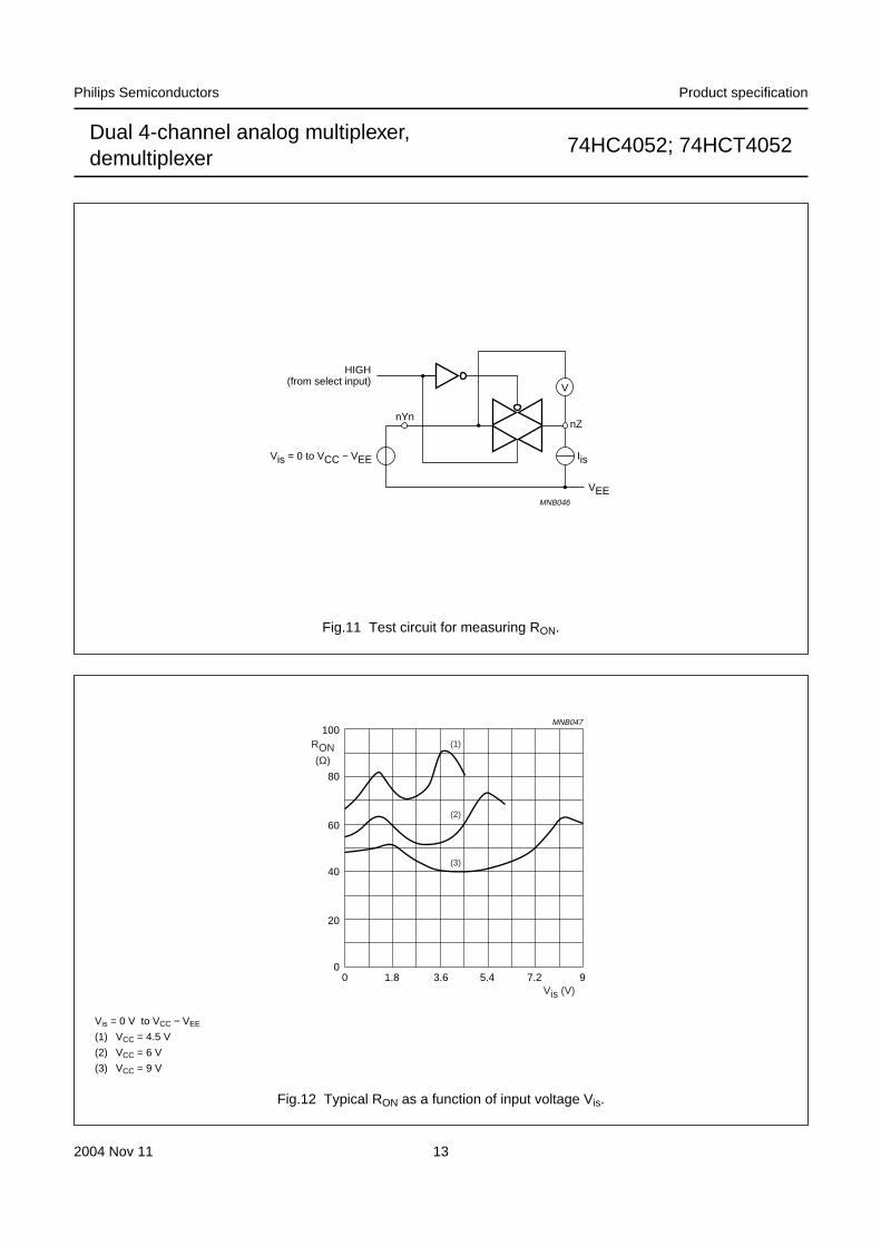
handbook, full pagewidth
MNB046
V
nYnnZ
IisVis = 0 to VCC − VEE
HIGH(from select input)
VEE
Fig.11 Test circuit for measuring RON.
handbook, halfpage
0 9
100
0
20
40
60
80
1.8 3.6 5.4 7.2
MNB047
RON(Ω)
Vis (V)
(1)
(2)
(3)
Fig.12 Typical RON as a function of input voltage Vis.
Vis = 0 V to VCC − VEE
(1) VCC = 4.5 V
(2) VCC = 6 V
(3) VCC = 9 V
2004 Nov 11 13
Philips Semiconductors Product specification
Dual 4-channel analog multiplexer,demultiplexer
74HC4052; 74HCT4052
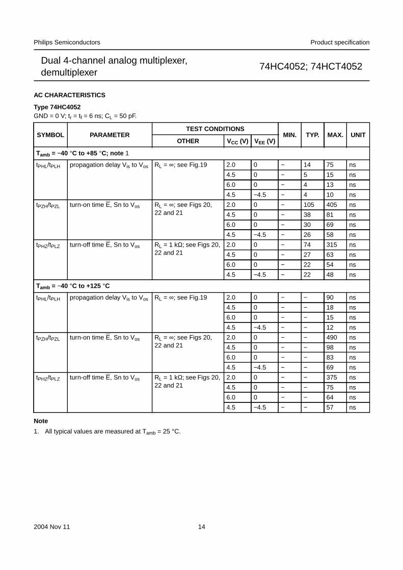
AC CHARACTERISTICS
Type 74HC4052GND = 0 V; tr = tf = 6 ns; CL = 50 pF.
Note
1. All typical values are measured at Tamb = 25 °C.
SYMBOL PARAMETERTEST CONDITIONS
MIN. TYP. MAX. UNITOTHER VCC (V) VEE (V)
Tamb = −40 °C to +85 °C; note 1
tPHL/tPLH propagation delay Vis to Vos RL = ∞; see Fig.19 2.0 0 − 14 75 ns
4.5 0 − 5 15 ns
6.0 0 − 4 13 ns
4.5 −4.5 − 4 10 ns
tPZH/tPZL turn-on time E, Sn to Vos RL = ∞; see Figs 20,22 and 21
2.0 0 − 105 405 ns
4.5 0 − 38 81 ns
6.0 0 − 30 69 ns
4.5 −4.5 − 26 58 ns
tPHZ/tPLZ turn-off time E, Sn to Vos RL = 1 kΩ; see Figs 20,22 and 21
2.0 0 − 74 315 ns
4.5 0 − 27 63 ns
6.0 0 − 22 54 ns
4.5 −4.5 − 22 48 ns
Tamb = −40 °C to +125 °C
tPHL/tPLH propagation delay Vis to Vos RL = ∞; see Fig.19 2.0 0 − − 90 ns
4.5 0 − − 18 ns
6.0 0 − − 15 ns
4.5 −4.5 − − 12 ns
tPZH/tPZL turn-on time E, Sn to Vos RL = ∞; see Figs 20,22 and 21
2.0 0 − − 490 ns
4.5 0 − − 98 ns
6.0 0 − − 83 ns
4.5 −4.5 − − 69 ns
tPHZ/tPLZ turn-off time E, Sn to Vos RL = 1 kΩ; see Figs 20,22 and 21
2.0 0 − − 375 ns
4.5 0 − − 75 ns
6.0 0 − − 64 ns
4.5 −4.5 − − 57 ns
2004 Nov 11 14
Philips Semiconductors Product specification
Dual 4-channel analog multiplexer,demultiplexer
74HC4052; 74HCT4052
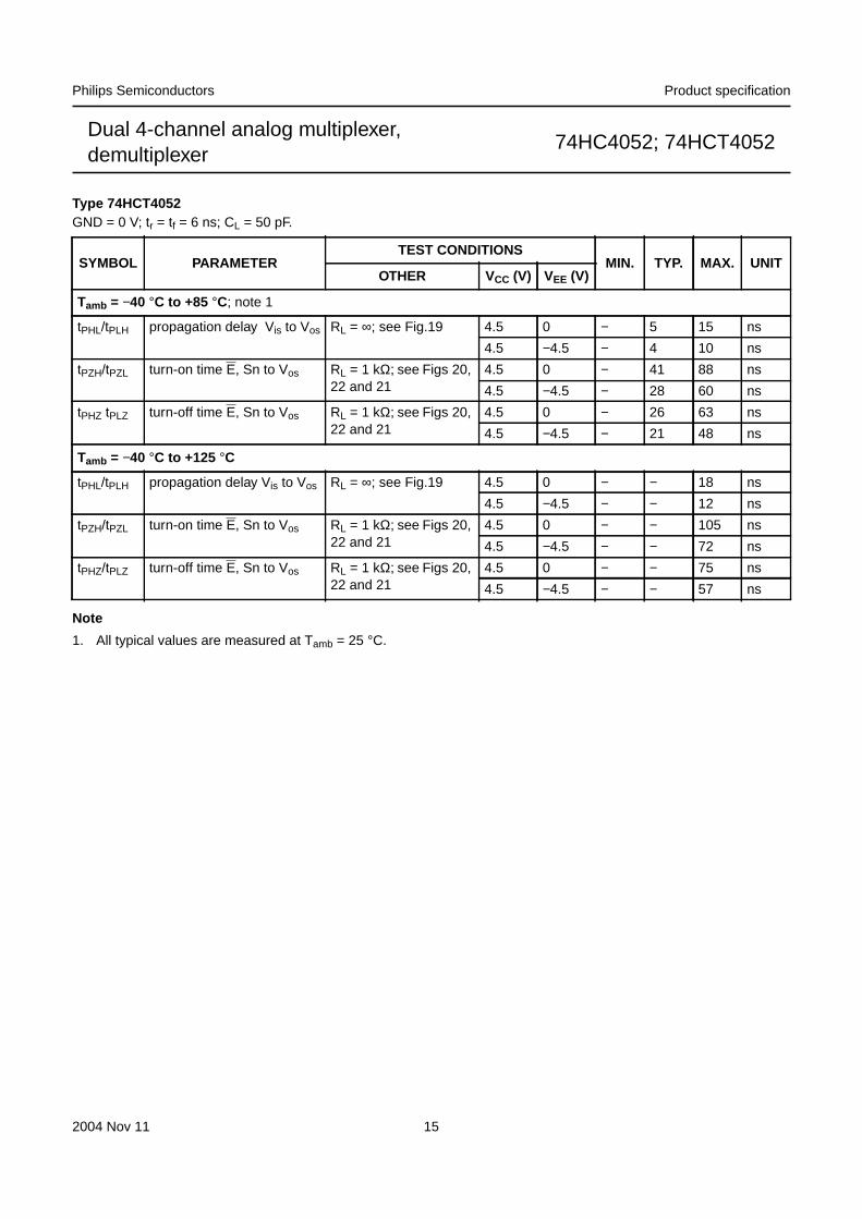
Type 74HCT4052GND = 0 V; tr = tf = 6 ns; CL = 50 pF.
Note
1. All typical values are measured at Tamb = 25 °C.
SYMBOL PARAMETERTEST CONDITIONS
MIN. TYP. MAX. UNITOTHER VCC (V) VEE (V)
Tamb = −40 °C to +85 °C; note 1
tPHL/tPLH propagation delay Vis to Vos RL = ∞; see Fig.19 4.5 0 − 5 15 ns
4.5 −4.5 − 4 10 ns
tPZH/tPZL turn-on time E, Sn to Vos RL = 1 kΩ; see Figs 20,22 and 21
4.5 0 − 41 88 ns
4.5 −4.5 − 28 60 ns
tPHZ tPLZ turn-off time E, Sn to Vos RL = 1 kΩ; see Figs 20,22 and 21
4.5 0 − 26 63 ns
4.5 −4.5 − 21 48 ns
Tamb = −40 °C to +125 °C
tPHL/tPLH propagation delay Vis to Vos RL = ∞; see Fig.19 4.5 0 − − 18 ns
4.5 −4.5 − − 12 ns
tPZH/tPZL turn-on time E, Sn to Vos RL = 1 kΩ; see Figs 20,22 and 21
4.5 0 − − 105 ns
4.5 −4.5 − − 72 ns
tPHZ/tPLZ turn-off time E, Sn to Vos RL = 1 kΩ; see Figs 20,22 and 21
4.5 0 − − 75 ns
4.5 −4.5 − − 57 ns
2004 Nov 11 15
Philips Semiconductors Product specification
Dual 4-channel analog multiplexer,demultiplexer
74HC4052; 74HCT4052
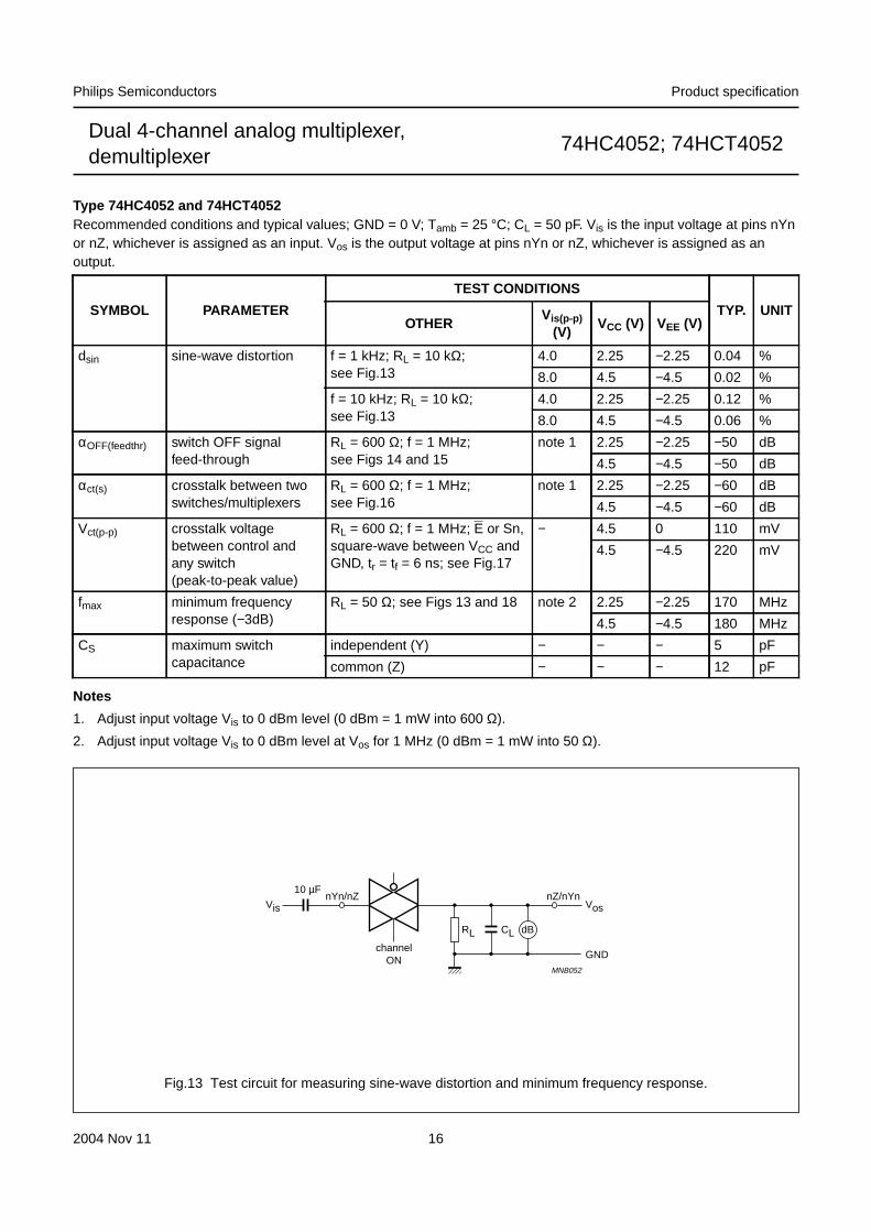
Type 74HC4052 and 74HCT4052Recommended conditions and typical values; GND = 0 V; Tamb = 25 °C; CL = 50 pF. Vis is the input voltage at pins nYnor nZ, whichever is assigned as an input. Vos is the output voltage at pins nYn or nZ, whichever is assigned as anoutput.
Notes
1. Adjust input voltage Vis to 0 dBm level (0 dBm = 1 mW into 600 Ω).
2. Adjust input voltage Vis to 0 dBm level at Vos for 1 MHz (0 dBm = 1 mW into 50 Ω).
SYMBOL PARAMETER
TEST CONDITIONS
TYP. UNITOTHER
Vis(p-p)(V)
VCC (V) VEE (V)
dsin sine-wave distortion f = 1 kHz; RL = 10 kΩ;see Fig.13
4.0 2.25 −2.25 0.04 %
8.0 4.5 −4.5 0.02 %
f = 10 kHz; RL = 10 kΩ;see Fig.13
4.0 2.25 −2.25 0.12 %
8.0 4.5 −4.5 0.06 %
αOFF(feedthr) switch OFF signalfeed-through
RL = 600 Ω; f = 1 MHz;see Figs 14 and 15
note 1 2.25 −2.25 −50 dB
4.5 −4.5 −50 dB
αct(s) crosstalk between twoswitches/multiplexers
RL = 600 Ω; f = 1 MHz;see Fig.16
note 1 2.25 −2.25 −60 dB
4.5 −4.5 −60 dB
Vct(p-p) crosstalk voltagebetween control andany switch(peak-to-peak value)
RL = 600 Ω; f = 1 MHz; E or Sn,square-wave between VCC andGND, tr = tf = 6 ns; see Fig.17
− 4.5 0 110 mV
4.5 −4.5 220 mV
fmax minimum frequencyresponse (−3dB)
RL = 50 Ω; see Figs 13 and 18 note 2 2.25 −2.25 170 MHz
4.5 −4.5 180 MHz
CS maximum switchcapacitance
independent (Y) − − − 5 pF
common (Z) − − − 12 pF
handbook, full pagewidth
MNB052
10 µF
RL
VosVis
CL dB
nZ/nYnnYn/nZ
GNDchannel
ON
Fig.13 Test circuit for measuring sine-wave distortion and minimum frequency response.
2004 Nov 11 16
Philips Semiconductors Product specification
Dual 4-channel analog multiplexer,demultiplexer
74HC4052; 74HCT4052
Fig.14 Test circuit for measuring switch OFF signal feed-through.
handbook, full pagewidth
MNB053
0.1 µF
RL
VosVis
CL dB
nZ/nYnnYn/nZ
GNDchannel
OFF
handbook, full pagewidth0
−20
−40
−60
−80
−100
MNB050
10 10 2 10 3 10 4 10 5 10 6f (kHz)
(dB)
Fig.15 Typical switch OFF signal feed-through as a function of frequency.
Test conditions: VCC = 4.5 V; GND = 0 V; VEE = −4.5 V; RL = 50 Ω; Rsource = 1 kΩ.
handbook, full pagewidth
MNB054
RL
RL0.1 µF nZ/nYnnYn/nZ
channelON
(a)
CL
GND
Vis
RLRL
nZ/nYnnYn/nZ
channelOFF
(b)
CL
GND
Vos
dB
Fig.16 Test circuits for measuring crosstalk between any two switches/multiplexers.
(a) channel ON condition. (b) channel OFF condition.
2004 Nov 11 17
Philips Semiconductors Product specification
Dual 4-channel analog multiplexer,demultiplexer
74HC4052; 74HCT4052
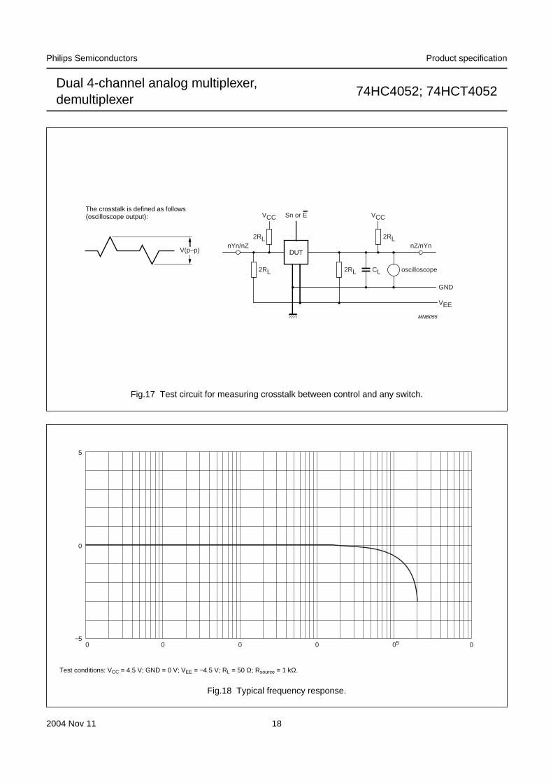
handbook, full pagewidth
DUT
MNB055
2RL2RL
2RL2RLnZ/nYnnYn/nZ
CL oscilloscope
VCC VCC
GND
VEE
V(p−p)
Sn or E
Fig.17 Test circuit for measuring crosstalk between control and any switch.
The crosstalk is defined as follows(oscilloscope output):
handbook, full pagewidth5
0
−5
MNB051
10 10 2 10 3 10 4 10 5 10 6f (kHz)
(dB)
Fig.18 Typical frequency response.
Test conditions: VCC = 4.5 V; GND = 0 V; VEE = −4.5 V; RL = 50 Ω; Rsource = 1 kΩ.
2004 Nov 11 18

Philips Semiconductors Product specification
Dual 4-channel analog multiplexer,demultiplexer
74HC4052; 74HCT4052
AC WAVEFORMS
handbook, halfpage
MNB056
tPLH tPHL
50%
50%Vis input
Vos output
GND
VI
VOH
VOL
Fig.19 Waveforms showing the input (Vis) to output (Vos) propagation delays.
handbook, full pagewidth
MNB057
tPLZ
tr tf
tPHZ
switchOFF
switchON
switchON
Vos output
Vos output
E, Sn input VM10%
90%
90%
10%
tPZL
tPZH
50%
50%
Fig.20 Waveforms showing the turn-on and turn-off times.
For 74HC4052: VM = 50 %; VI = GND to VCC.
For 74HCT4052: VM = 1.3 V; VI = GND to 3 V.
2004 Nov 11 19
Philips Semiconductors Product specification
Dual 4-channel analog multiplexer,demultiplexer
74HC4052; 74HCT4052
handbook, full pagewidth
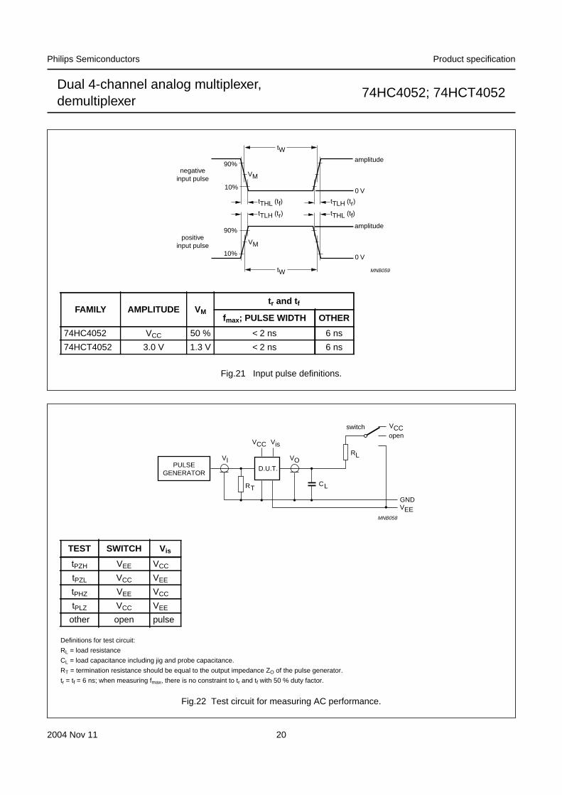
MNB059
tTHL (tf) tTLH (tr)
VM
tW
positiveinput pulse
negativeinput pulse
0 V
amplitude90%
10%
tTLH (tr) tTHL (tf)
VM
tW
0 V
amplitude90%
10%
Fig.21 Input pulse definitions.
FAMILY AMPLITUDE V M
tr and t f
fmax; PULSE WIDTH OTHER
74HC4052 VCC 50 % < 2 ns 6 ns
74HCT4052 3.0 V 1.3 V < 2 ns 6 ns
handbook, full pagewidth
openswitch VCC
VEE
GND
VCC Vis
VI VO
MNB058
D.U.T.
CLRT
RL
PULSEGENERATOR
Fig.22 Test circuit for measuring AC performance.
TEST SWITCH Vis
tPZH VEE VCC
tPZL VCC VEE
tPHZ VEE VCC
tPLZ VCC VEE
other open pulse
Definitions for test circuit:
RL = load resistance
CL = load capacitance including jig and probe capacitance.
RT = termination resistance should be equal to the output impedance ZO of the pulse generator.
tr = tf = 6 ns; when measuring fmax, there is no constraint to tr and tf with 50 % duty factor.
2004 Nov 11 20
Philips Semiconductors Product specification
Dual 4-channel analog multiplexer,demultiplexer
74HC4052; 74HCT4052
PACKAGE OUTLINES
REFERENCESOUTLINEVERSION
EUROPEANPROJECTION ISSUE DATE
IEC JEDEC JEITA
SOT38-9 97-07-2403-03-12
MH
c
ME
A
L
seat
ing
plan
e
w Me
D
A2
A1
b1
b2
Z
16
1
9
8
E
pin 1 index
b
0 5 10 mm
scale
Note
1. Plastic or metal protrusions of 0.25 mm (0.01 inch) maximum per side are not included.
UNIT Amax. b1
(1) (1) (1)b2 c D E e MH
ZL
mm
DIMENSIONS (mm dimensions are derived from the original inch dimensions)
A1 min.
A2 max.
bmax.
wMEe1
1.651.40
0.510.41
0.360.20
19.318.8
6.456.24
3.812.92
0.2542.54 7.628.237.62
9.408.38
0.764.32 0.38 3.56
inches 0.0650.055
0.0200.016
0.0140.008
1.140.76
0.0450.030
0.760.74
0.2540.246
0.1500.115
0.010.1 0.30.3240.300
0.370.33
0.030.17 0.015 0.14
DIP16: plastic dual in-line package; 16 leads (300 mil) SOT38-9
(e1)
2004 Nov 11 21
Philips Semiconductors Product specification
Dual 4-channel analog multiplexer,demultiplexer
74HC4052; 74HCT4052
X
w M
θ
AA1
A2
bp
D
HE
Lp
detail X
E
Z
e
c
L
v M A
(A )3
A
8
9
1
16
y
pin 1 index
UNITA
max. A1 A2 A3 bp c D (1) E(1) (1)e HE L L p Zywv θ
REFERENCESOUTLINEVERSION
EUROPEANPROJECTION ISSUE DATE
IEC JEDEC JEITA
mm
inches
1.750.250.10
1.551.40
0.250.490.36
0.250.19
10.09.8
4.03.8
1.276.25.8
0.70.3 8
0
o
o
0.25 0.1
DIMENSIONS (inch dimensions are derived from the original mm dimensions)
Note
1. Plastic or metal protrusions of 0.15 mm (0.006 inch) maximum per side are not included.
1.00.4
SOT109-3 98-12-2303-02-19
MS-012AC
0.0690.0100.004
0.0610.055
0.010.0190.014
0.01000.0075
0.390.38
0.160.15
0.05
1.05
0.0410.2440.228
0.0280.012
0.01
0.25
0.01 0.0040.0390.016
0 2.5 5 mm
scale
SO16: plastic small outline package; 16 leads; body width 3.9 mm; body thickness 1.47 mm SOT109-3
2004 Nov 11 22
Philips Semiconductors Product specification
Dual 4-channel analog multiplexer,demultiplexer
74HC4052; 74HCT4052
UNIT A1 A2 A3 bp c D (1) E (1) e HE L L p Q Zywv θ
REFERENCESOUTLINEVERSION
EUROPEANPROJECTION ISSUE DATE
IEC JEDEC JEITA
mm 0.210.05
1.801.65
0.250.380.25
0.200.09
6.46.0
5.45.2
0.65 1.257.97.6
1.030.63
0.90.7
1.000.55
80
o
o0.130.2 0.1
DIMENSIONS (mm are the original dimensions)
Note
1. Plastic or metal protrusions of 0.25 mm maximum per side are not included.
SOT338-199-12-2703-02-19
(1)
w Mbp
D
HE
E
Z
e
c
v M A
XA
y
1 8
16 9
θ
AA1
A2
Lp
Q
detail X
L
(A )3
MO-150
pin 1 index
0 2.5 5 mm
scale
SSOP16: plastic shrink small outline package; 16 leads; body width 5.3 mm SOT338-1
Amax.
2
2004 Nov 11 23
Philips Semiconductors Product specification
Dual 4-channel analog multiplexer,demultiplexer
74HC4052; 74HCT4052
UNIT A1 A2 A3 bp c D (1) E (2) (1)e HE L L p Q Zywv θ
REFERENCESOUTLINEVERSION
EUROPEANPROJECTION ISSUE DATE
IEC JEDEC JEITA
mm 0.150.05
0.950.80
0.300.19
0.20.1
5.14.9
4.54.3
0.656.66.2
0.40.3
0.400.06
80
o
o0.13 0.10.21
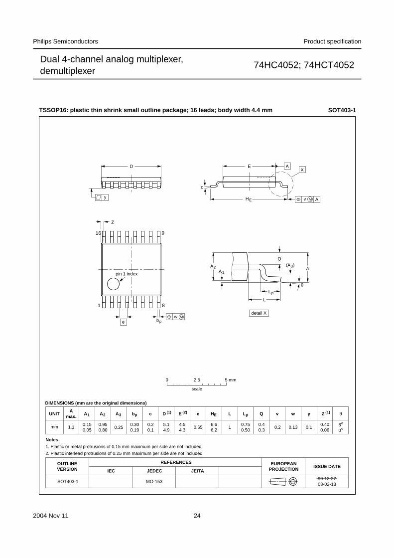
DIMENSIONS (mm are the original dimensions)
Notes
1. Plastic or metal protrusions of 0.15 mm maximum per side are not included.
2. Plastic interlead protrusions of 0.25 mm maximum per side are not included.
0.750.50
SOT403-1 MO-15399-12-2703-02-18
w Mbp
D
Z
e
0.25
1 8
16 9
θ
AA1
A2
Lp
Q
detail X
L
(A )3
HE
E
c
v M A
XA
y
0 2.5 5 mm
scale
TSSOP16: plastic thin shrink small outline package; 16 leads; body width 4.4 mm SOT403-1
Amax.
1.1
pin 1 index
2004 Nov 11 24
Philips Semiconductors Product specification
Dual 4-channel analog multiplexer,demultiplexer
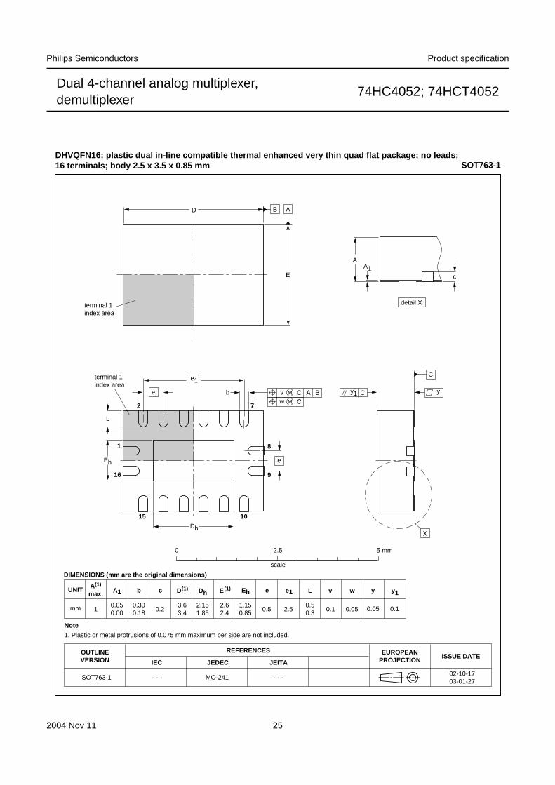
74HC4052; 74HCT4052
terminal 1index area
0.51
A1 EhbUNIT ye
0.2
c
REFERENCESOUTLINEVERSION
EUROPEANPROJECTION ISSUE DATE
IEC JEDEC JEITA
mm 3.63.4
Dh
2.151.85
y1
2.62.4
1.150.85
e1
2.50.300.18
0.050.00
0.05 0.1
DIMENSIONS (mm are the original dimensions)
SOT763-1 MO-241 - - -- - -
0.50.3
L
0.1
v
0.05
w
0 2.5 5 mm
scale
SOT763-1DHVQFN16: plastic dual in-line compatible thermal enhanced very thin quad flat package; no leads;16 terminals; body 2.5 x 3.5 x 0.85 mm
A(1)
max.
AA1
c
detail X
yy1 Ce
L
Eh
Dh
e
e1
b
2 7
15 10
9
81
16
X
D
E
C
B A
terminal 1index area
ACC
Bv M
w M
E(1)
Note
1. Plastic or metal protrusions of 0.075 mm maximum per side are not included.
D(1)
02-10-1703-01-27
2004 Nov 11 25
Philips Semiconductors Product specification
Dual 4-channel analog multiplexer,demultiplexer
74HC4052; 74HCT4052
DATA SHEET STATUS
Notes
1. Please consult the most recently issued data sheet before initiating or completing a design.
2. The product status of the device(s) described in this data sheet may have changed since this data sheet waspublished. The latest information is available on the Internet at URL http://www.semiconductors.philips.com.
3. For data sheets describing multiple type numbers, the highest-level product status determines the data sheet status.
LEVELDATA SHEET
STATUS(1)PRODUCT
STATUS(2)(3) DEFINITION
I Objective data Development This data sheet contains data from the objective specification for productdevelopment. Philips Semiconductors reserves the right to change thespecification in any manner without notice.
II Preliminary data Qualification This data sheet contains data from the preliminary specification.Supplementary data will be published at a later date. PhilipsSemiconductors reserves the right to change the specification withoutnotice, in order to improve the design and supply the best possibleproduct.
III Product data Production This data sheet contains data from the product specification. PhilipsSemiconductors reserves the right to make changes at any time in orderto improve the design, manufacturing and supply. Relevant changes willbe communicated via a Customer Product/Process Change Notification(CPCN).
DEFINITIONS
Short-form specification The data in a short-formspecification is extracted from a full data sheet with thesame type number and title. For detailed information seethe relevant data sheet or data handbook.
Limiting values definition Limiting values given are inaccordance with the Absolute Maximum Rating System(IEC 60134). Stress above one or more of the limitingvalues may cause permanent damage to the device.These are stress ratings only and operation of the deviceat these or at any other conditions above those given in theCharacteristics sections of the specification is not implied.Exposure to limiting values for extended periods mayaffect device reliability.
Application information Applications that aredescribed herein for any of these products are forillustrative purposes only. Philips Semiconductors makeno representation or warranty that such applications will besuitable for the specified use without further testing ormodification.
DISCLAIMERS
Life support applications These products are notdesigned for use in life support appliances, devices, orsystems where malfunction of these products canreasonably be expected to result in personal injury. PhilipsSemiconductors customers using or selling these productsfor use in such applications do so at their own risk andagree to fully indemnify Philips Semiconductors for anydamages resulting from such application.
Right to make changes Philips Semiconductorsreserves the right to make changes in the products -including circuits, standard cells, and/or software -described or contained herein in order to improve designand/or performance. When the product is in full production(status ‘Production’), relevant changes will becommunicated via a Customer Product/Process ChangeNotification (CPCN). Philips Semiconductors assumes noresponsibility or liability for the use of any of theseproducts, conveys no licence or title under any patent,copyright, or mask work right to these products, andmakes no representations or warranties that theseproducts are free from patent, copyright, or mask workright infringement, unless otherwise specified.
2004 Nov 11 26

© Koninklijke Philips Electronics N.V. 2004 SCA76All rights are reserved. Reproduction in whole or in part is prohibited without the prior written consent of the copyright owner.
The information presented in this document does not form part of any quotation or contract, is believed to be accurate and reliable and may be changedwithout notice. No liability will be accepted by the publisher for any consequence of its use. Publication thereof does not convey nor imply any license
Philips Semiconductors – a worldwide company
Contact information
For additional information please visit http://www.semiconductors.philips.com . Fax: +31 40 27 24825For sales offices addresses send e-mail to: [email protected] .
under patent- or other industrial or intellectual property rights.
Printed in The Netherlands R44/04/pp27 Date of release: 2004 Nov 11 Document order number: 9397 750 14189


![A Novel Digital Calibration Technique for Gain and Offset ......ΣΔ modulators. The input signal x[n] is distributed among the M modulators through an analog multiplexer. Then, the](https://static.fdocument.org/doc/165x107/60ee77b99c0fd85f564bb9e6/a-novel-digital-calibration-technique-for-gain-and-offset-modulators.jpg)