FSA2567 Low-Power, Dual SIM Card Analog Switch
13
February 2015 © 2008 Fairchild Semiconductor Corporation www.fairchildsemi.com FSA2567 Rev. 1.13 FSA2567 — Low-Power, Dual SIM Card Analog Switch FSA2567 — Low-Power, Dual SIM Card Analog Switch Features Low On Capacitance for Data Path: 10 pF Typical Low On Resistance for Data Path: 6 Ω Typical Low On Resistance for Supply Path: 0.4 Ω Typical Wide VCC Operating Range: 1.65 V to 4.3 V Low Power Consumption: 1 μA Maximum - 15 μA Maximum ICCT Over Expanded Voltage Range (VIN=1.8 V, VCC=4.3 V) Wide -3 db Bandwidth: > 160 MHz Packaged in: - Pb-free 16-Lead MLP & 16-Lead UMLP 3 kV ESD Rating, >12 kV Power/GND ESD Rating Applications Cell phone, PDA, Digital Camera, and Notebook LCD Monitor, TV, and Set-Top Box Description The FSA2567 is a bi-directional, low-power, dual double-pole, double-throw (4PDT) analog switch targeted at dual SIM card multiplexing. It is optimized for switching the WLAN-SIM data and control signals and dedicates one channel as a supply-source switch. The FSA2567 is compatible with the requirements of SIM cards and features a low on capacitance (CON) of 10 pF to ensure high-speed data transfer. The VSIM switch path has a low RON characteristic to ensure minimal voltage drop in the dual SIM card supply paths. The FSA2567 contains special circuitry that minimizes current consumption when the control voltage applied to the SEL pin is lower than the supply voltage (VCC). This feature is especially valuable in ultra-portable applications, such as cell phones; allowing direct interface with the general-purpose I/Os of the baseband processor. Other applications include switching and connector sharing in portable cell phones, PDAs, digital cameras, printers, and notebook computers. Ordering Information Part Number Top Mark Operating Temperature Range Package FSA2567MPX FSA2567 -40 to +85°C 16-Lead, Molded Leadless Package (MLP) Quad, JEDEC MO-220, 3 mm Square FSA2567UMX GX 16-Lead, Quad, Ultrathin Molded Leadless Package (UMLP), 1.8 x 2.6 mm For Fairchild’s definition of Eco Status, please visit: http://www.fairchildsemi.com/company/green/rohs_green.html . 1V SIM 2V SIM V SIM 1RST 2RST RST Sel 1CLK 2CLK CLK 2DAT DAT 1DAT Figure 1. Analog Symbol
Transcript of FSA2567 Low-Power, Dual SIM Card Analog Switch
February 2015
© 2008 Fairchild Semiconductor Corporation www.fairchildsemi.com FSA2567 Rev. 1.13
FS
A2
56
7 —
Lo
w-P
ow
er, D
ual S
IM C
ard
An
alo
g S
witc
h
FSA2567 — Low-Power, Dual SIM Card Analog Switch
Features
Low On Capacitance for Data Path: 10 pF Typical
Low On Resistance for Data Path: 6 Ω Typical
Low On Resistance for Supply Path: 0.4 Ω Typical
Wide VCC Operating Range: 1.65 V to 4.3 V
Low Power Consumption: 1 μA Maximum
- 15 μA Maximum ICCT Over Expanded Voltage Range (VIN=1.8 V, VCC=4.3 V)
Wide -3 db Bandwidth: > 160 MHz
Packaged in:
- Pb-free 16-Lead MLP & 16-Lead UMLP
3 kV ESD Rating, >12 kV Power/GND ESD Rating
Applications
Cell phone, PDA, Digital Camera, and Notebook
LCD Monitor, TV, and Set-Top Box
Description
The FSA2567 is a bi-directional, low-power, dual double-pole, double-throw (4PDT) analog switch targeted at dual SIM card multiplexing. It is optimized for switching the WLAN-SIM data and control signals and dedicates one channel as a supply-source switch.
The FSA2567 is compatible with the requirements of SIM cards and features a low on capacitance (CON) of 10 pF to ensure high-speed data transfer. The VSIM switch path has a low RON characteristic to ensure minimal voltage drop in the dual SIM card supply paths.
The FSA2567 contains special circuitry that minimizes current consumption when the control voltage applied to the SEL pin is lower than the supply voltage (VCC). This feature is especially valuable in ultra-portable applications, such as cell phones; allowing direct interface with the general-purpose I/Os of the baseband processor. Other applications include switching and connector sharing in portable cell phones, PDAs, digital cameras, printers, and notebook computers.
Ordering Information
Part Number Top Mark
Operating
Temperature
Range
Package
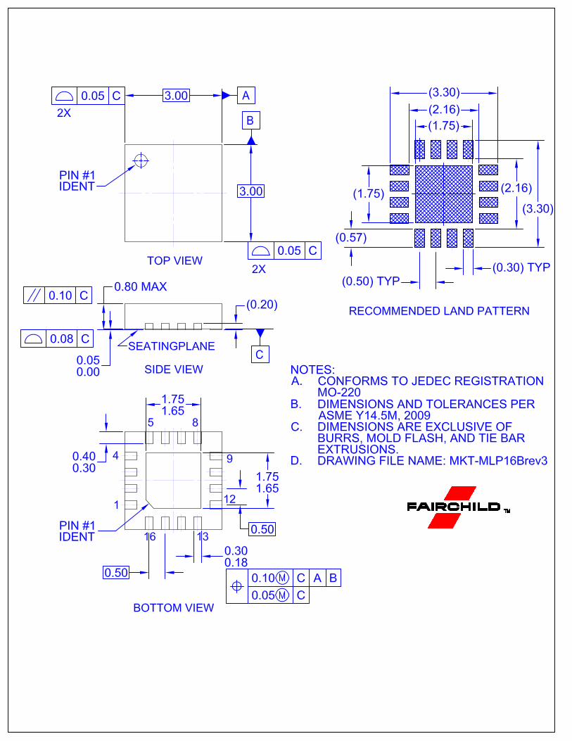
FSA2567MPX FSA2567 -40 to +85°C 16-Lead, Molded Leadless Package (MLP) Quad, JEDEC MO-220, 3 mm Square
FSA2567UMX GX 16-Lead, Quad, Ultrathin Molded Leadless Package (UMLP), 1.8 x 2.6 mm
For Fairchild’s definition of Eco Status, please visit: http://www.fairchildsemi.com/company/green/rohs_green.html.
1VSIM
2VSIM
VSIM
1RST
2RSTRST
Sel
1CLK
2CLKCLK
2DATDAT
1DAT
Figure 1. Analog Symbol
© 2008 Fairchild Semiconductor Corporation www.fairchildsemi.com FSA2567 Rev. 1.13 2
FS
A2
56
7 —
Lo
w-P
ow
er, D
ual S
IM C
ard
An
alo
g S
witc
h
Pin Assignments
VC
C
1CLK
2RST2C
LK
1D
AT
1R
ST
2V
SIM
VS
IM1V
SIM
CLK
RST
No Connect
Sel
DAT
GN
D2DAT11
3 10
9
8765
4
2
1
16 131415
12
(Not connected to GND)
1CLK
2RST
2C
LK
1R
ST
CLK
RST
No Connect
GN
D
1D
AT
VC
C
2V
SIM
VS
IM
15 131416
6 875
3
94
1VSIM DAT1 12
Sel 2DAT2 11
10
Figure 2. Pad Assignment MLP16
(Top Through View)
Figure 3. Pad Assignment UMLP16
(Top Through View)
Pin Definitions
Pin Description
nDAT, nRST, nCLK Multiplexed Data Source Inputs
nVSIM Multiplexed SIM Supply Inputs
VSIM , DAT, RST, CLK Common SIM Ports
Sel Switch Select
Truth Table
Sel Function
Logic LOW 1DAT = DAT, 1RST = RST, 1CLK = CLK, 1VSIM = VSIM
Logic HIGH 2DAT = DAT, 2RST = RST, 2CLK = CLK, 2VSIM = VSIM
© 2008 Fairchild Semiconductor Corporation www.fairchildsemi.com FSA2567 Rev. 1.13 3
FS
A2
56
7 —
Lo
w-P
ow
er, D
ual S
IM C
ard
An
alo
g S
witc
h
Absolute Maximum Ratings
Stresses exceeding the absolute maximum ratings may damage the device. The device may not function or be operable above the recommended operating conditions and stressing the parts to these levels is not recommended. In addition, extended exposure to stresses above the recommended operating conditions may affect device reliability. The absolute maximum ratings are stress ratings only.
Symbol Parameter Min. Max. Unit
VCC Supply Voltage -0.5 +5.5 V
VCNTRL DC Input Voltage (Sel)(1)
-0.5 VCC V
VSW DC Switch I/O Voltage(1)
-0.5 VCC + 0.3 V
IIK DC Input Diode Current -50 mA
ISIM DC Output Current - VSIM 350 mA
IOUT DC Output Current – DAT, CLK, RST 35 mA
TSTG Storage Temperature -65 +150 °C
ESD Human Body Model, JEDEC: JESD22-A114
All Pins 3
kV I/O to GND 12
Charged Device Model, JEDEC: JESD22-C101 2
Note: 1. The input and output negative ratings may be exceeded if the input and output diode current ratings are
observed.
Recommended Operating Conditions
The Recommended Operating Conditions table defines the conditions for actual device operation. Recommended operating conditions are specified to ensure optimal performance to the datasheet specifications. Fairchild does not recommend exceeding them or designing to Absolute Maximum Ratings.
Symbol Parameter Min. Max. Unit
VCC Supply Voltage 1.65 4.30 V
VCNTRL
Control Input Voltage (Sel)(2)
0 VCC V
VSW Switch I/O Voltage -0.5 VCC V
ISIM DC Output Current - VSIM 150 mA
IOUT DC Output Current – DAT, CLK, RST 25 mA
TA Operating Temperature -40 +85 °C
Note: 2. The control input must be held HIGH or LOW; it must not float.
© 2008 Fairchild Semiconductor Corporation www.fairchildsemi.com FSA2567 Rev. 1.13 4
FS
A2
56
7 —
Lo
w-P
ow
er, D
ual S
IM C
ard
An
alo
g S
witc
h
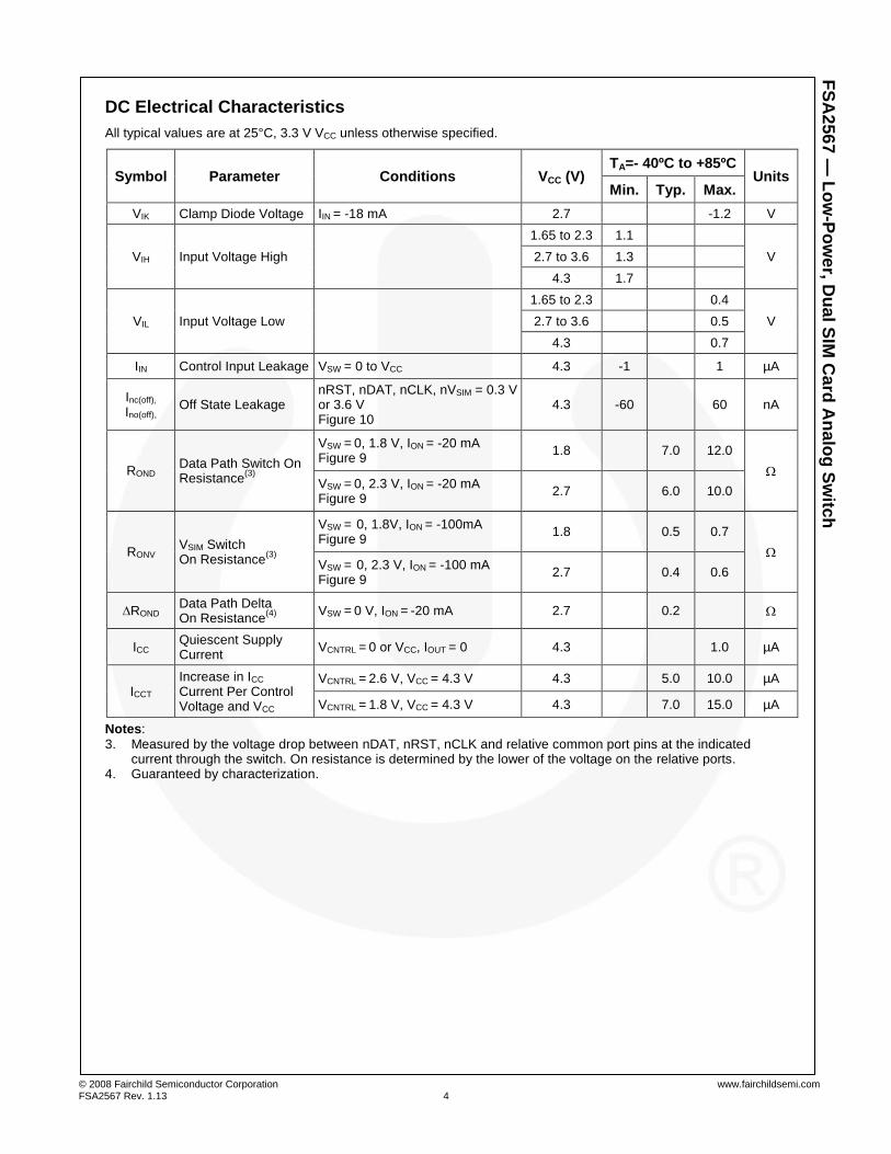
DC Electrical Characteristics
All typical values are at 25°C, 3.3 V VCC unless otherwise specified.
Symbol Parameter Conditions VCC (V) TA=- 40ºC to +85ºC
Units Min. Typ. Max.
VIK Clamp Diode Voltage IIN = -18 mA 2.7 -1.2 V
VIH Input Voltage High
1.65 to 2.3 1.1
V 2.7 to 3.6 1.3
4.3 1.7
VIL Input Voltage Low
1.65 to 2.3 0.4
V 2.7 to 3.6 0.5
4.3 0.7
IIN Control Input Leakage VSW = 0 to VCC 4.3 -1 1 µA
Inc(off),
Ino(off), Off State Leakage
nRST, nDAT, nCLK, nVSIM = 0.3 V or 3.6 V
Figure 10 4.3 -60 60 nA
ROND Data Path Switch On Resistance
(3)
VSW = 0, 1.8 V, ION = -20 mA Figure 9
1.8 7.0 12.0
VSW = 0, 2.3 V, ION = -20 mA Figure 9
2.7 6.0 10.0
RONV VSIM Switch On Resistance
(3)
VSW = 0, 1.8V, ION = -100mA Figure 9
1.8 0.5 0.7
VSW = 0, 2.3 V, ION = -100 mA Figure 9
2.7 0.4 0.6
∆ROND Data Path Delta On Resistance
(4)
VSW = 0 V, ION = -20 mA 2.7 0.2
ICC Quiescent Supply Current
VCNTRL = 0 or VCC, IOUT = 0 4.3 1.0 µA
ICCT Increase in ICC
Current Per Control Voltage and VCC
VCNTRL = 2.6 V, VCC = 4.3 V 4.3 5.0 10.0 µA
VCNTRL = 1.8 V, VCC = 4.3 V 4.3 7.0 15.0 µA
Notes: 3. Measured by the voltage drop between nDAT, nRST, nCLK and relative common port pins at the indicated
current through the switch. On resistance is determined by the lower of the voltage on the relative ports. 4. Guaranteed by characterization.
© 2008 Fairchild Semiconductor Corporation www.fairchildsemi.com FSA2567 Rev. 1.13 5
FS
A2
56
7 —
Lo
w-P
ow
er, D
ual S
IM C
ard
An
alo
g S
witc
h
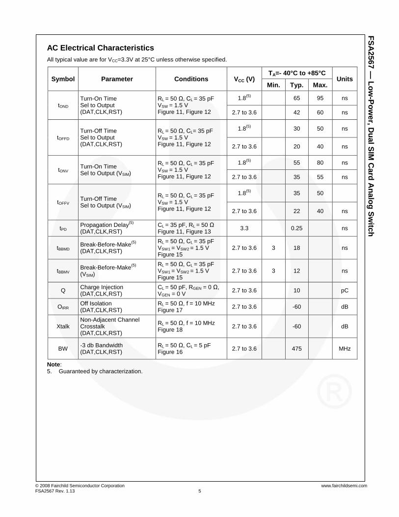
AC Electrical Characteristics
All typical value are for VCC=3.3V at 25°C unless otherwise specified.
Symbol Parameter Conditions VCC (V) TA=- 40°C to +85°C
Units Min. Typ. Max.
tOND Turn-On Time Sel to Output (DAT,CLK,RST)
RL = 50 Ω, CL = 35 pF VSW = 1.5 V Figure 11, Figure 12
1.8(5)
65 95 ns
2.7 to 3.6 42 60 ns
tOFFD Turn-Off Time Sel to Output (DAT,CLK,RST)
RL = 50 Ω, CL= 35 pF VSW = 1.5 V Figure 11, Figure 12
1.8(5)
30 50 ns
2.7 to 3.6 20 40 ns
tONV Turn-On Time Sel to Output (VSIM)
RL = 50 Ω, CL = 35 pF VSW = 1.5 V Figure 11, Figure 12
1.8(5)
55 80 ns
2.7 to 3.6 35 55 ns
tOFFV Turn-Off Time Sel to Output (VSIM)
RL = 50 Ω, CL = 35 pF VSW = 1.5 V Figure 11, Figure 12
1.8(5)
35 50
2.7 to 3.6 22 40 ns
tPD Propagation Delay
(5)
(DAT,CLK,RST)
CL = 35 pF, RL = 50 Ω Figure 11, Figure 13
3.3 0.25 ns
tBBMD Break-Before-Make
(5)
(DAT,CLK,RST)
RL = 50 Ω, CL = 35 pF VSW1 = VSW2 = 1.5 V Figure 15
2.7 to 3.6 3 18 ns
tBBMV Break-Before-Make
(5)
(VSIM)
RL = 50 Ω, CL = 35 pF VSW1 = VSW2 = 1.5 V Figure 15
2.7 to 3.6 3 12 ns
Q Charge Injection (DAT,CLK,RST)
CL = 50 pF, RGEN = 0 Ω, VGEN = 0 V
2.7 to 3.6 10 pC
OIRR Off Isolation (DAT,CLK,RST)
RL = 50 Ω, f = 10 MHz Figure 17
2.7 to 3.6 -60 dB
Xtalk Non-Adjacent Channel Crosstalk (DAT,CLK,RST)
RL = 50 Ω, f = 10 MHz Figure 18
2.7 to 3.6 -60 dB
BW -3 db Bandwidth (DAT,CLK,RST)
RL = 50 Ω, CL = 5 pF Figure 16
2.7 to 3.6 475 MHz
Note: 5. Guaranteed by characterization.
© 2008 Fairchild Semiconductor Corporation www.fairchildsemi.com FSA2567 Rev. 1.13 6
FS
A2
56
7 —
Lo
w-P
ow
er, D
ual S
IM C
ard
An
alo
g S
witc
h
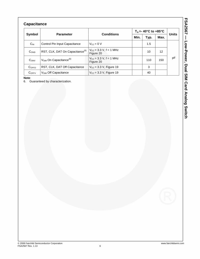
Capacitance
Symbol Parameter Conditions TA =- 40°C to +85°C
Units Min. Typ. Max.
CIN Control Pin Input Capacitance VCC = 0 V 1.5
pF
COND RST, CLK, DAT On Capacitance(6)
VCC = 3.3 V, f = 1 MHz Figure 20
10 12
CONV VSIM On Capacitance(6)
VCC = 3.3 V, f = 1 MHz Figure 20
110 150
COFFD RST, CLK, DAT Off Capacitance VCC = 3.3 V, Figure 19 3
COFFV VSIM Off Capacitance VCC = 3.3 V, Figure 19 40
Note: 6. Guaranteed by characterization.
© 2008 Fairchild Semiconductor Corporation www.fairchildsemi.com FSA2567 Rev. 1.13 7
FS
A2
56
7 —
Lo
w-P
ow
er, D
ual S
IM C
ard
An
alo
g S
witc
h
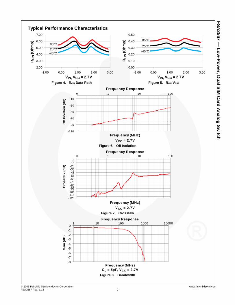
Typical Performance Characteristics
2.00
3.00
4.00
5.00
6.00
7.00
-1.00 0.00 1.00 2.00 3.00
VIN, VCC = 2.7V
RO
N(O
hm
s)
85°C
25°C
-40°C
0.00
0.10
0.20
0.30
0.40
0.50
-1.00 0.00 1.00 2.00 3.00
VIN, VCC = 2.7V
RO
N(O
hm
s) 85°C
25°C
-40°C
Figure 4. RON Data Path Figure 5. RON VSIM
Frequency Response
-110
-90
-70
-50
-30
-10
0 1 10 100
Frequency (MHz)
VCC = 2.7V
Off
Isola
tion
(dB
)
Figure 6. Off Isolation
-125-115-105-95-85-75-65-55-45-35-25-15-5
0 1 10 100
Cro
ssta
lk(d
B)
Frequency Response
Frequency (MHz)
VCC = 2.7V Figure 7. Crosstalk
-8
-7
-6
-5
-4
-3
-2
-1
01 10 100 1000 10000
Gain
(dB
)
Frequency Response
Frequency (MHz)
CL = 5pF, VCC = 2.7V Figure 8. Bandwidth
© 2008 Fairchild Semiconductor Corporation www.fairchildsemi.com FSA2567 Rev. 1.13 8
FS
A2
56
7 —
Lo
w-P
ow
er, D
ual S
IM C
ard
An
alo
g S
witc
h
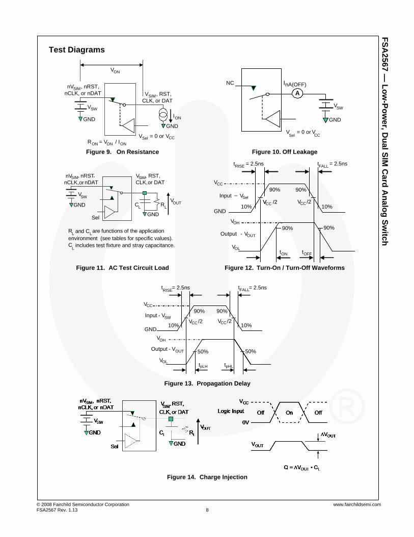
Test Diagrams
nVSIM, nRST,
nCLK, or nDAT
VSel = 0 or VCC
ION
VON
RON = VON / ION
GND
VSW
GND
V , RST,
CLK, or DATSIM
NC
A
InA(OFF)
VSW
GND
VSel
= 0 or VCC
Figure 9. On Resistance Figure 10. Off Leakage
RL
and CLare functions of the application
environment (see tables for specific values).
CL
includes test fixture and stray capacitance.
RL
CL
GND
VSW
GNDV
OUT
Sel
nVSIM, nRST
nCLK,or nDAT
VSIM, RST,
CLK,or DAT
,
tRISE
= 2.5ns
GND
VCC
90% 90%
10%10%
tFALL
= 2.5ns
V /2 VCC /2Input – VSel
Output - VOUT
90%
V
VOLtON tOFF
90%
VCC
OH
Figure 11. AC Test Circuit Load Figure 12. Turn-On / Turn-Off Waveforms
tRISE
= 2.5ns
GND
VCC
90% 90%
10%10%
tFALL= 2.5ns
VCC /2 VCC /2Input - VSW
Output VOUT 50% 50%
VOH
VOLtpLH tpHL
-
Figure 13. Propagation Delay
Figure 14. Charge Injection
© 2008 Fairchild Semiconductor Corporation www.fairchildsemi.com FSA2567 Rev. 1.13 9
FS
A2
56
7 —
Lo
w-P
ow
er, D
ual S
IM C
ard
An
alo
g S
witc
h
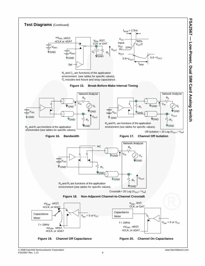
Test Diagrams (Continued)
tRISE= 2.5ns
VOUT
VCC
0.9 VOUT
VCC/2
tBBM
0V
V
Input-
VSel
0.9 • VOUT
90%
10%
CL RL
GND
VSW1
GND VSW2
GND
RL and CL are functions of the application
environment (see tables for specific values).
includes test fixture and stray capacitance.
nVSIM, nRST,
or nDAT VSIM ,RST,CLK or DAT
OUT
CL
nCLK
•
Sel
Figure 15. Break-Before-Make Interval Timing
VOUT
GND
RT
GND
GND
VS
RS
Network Analyzer
VSEL
RS
and RT are tifunc ons of the tapplica ionn re vi onment (see tables for specific values).
VIN
GNDGND
RSand RT are functions of the application
environment (see tables for specific values).
VOUT
RT
VS
RS
Network Analyzer
RT
VSel
VIN
Off isolation = 20 Log (VOUT / VIN)
GNDGND
GND
GND
GNDGND
Figure 16. Bandwidth Figure 17. Channel Off Isolation
VOUTGND RT
VS
RS
Network Analyzer
RT
RSand RT are functions of the application
VSel
NC
VIN
Crosstalk= 20 Log (VOUT / VIN)
environment (see tables for specific values).
GND
GND
GND
GND
GND
Figure 18. Non-Adjacent Channel-to-Channel Crosstalk
VSel = 0 orVCC
Capacitance
Meter
f = 1MHz
nVSIM, nRST
nCLK, or nDAT
nVSIM, nRST,nCLK, or nDAT
,
VSel = 0 or VCC
Capacitance
Meter
f = 1MHz
VSIM , RST,
CLK, or DAT
nVSIM nRST,
nCLK, or nDAT
,
Figure 19. Channel Off Capacitance Figure 20. Channel On Capacitance
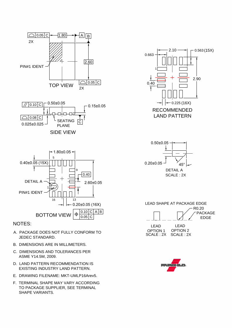
RECOMMENDED
LAND PATTERN
NOTES:
A. PACKAGE DOES NOT FULLY CONFORM TO
JEDEC STANDARD.
B. DIMENSIONS ARE IN MILLIMETERS.
C. DIMENSIONS AND TOLERANCES PER
ASME Y14.5M, 2009.
D. LAND PATTERN RECOMMENDATION IS
EXISTING INDUSTRY LAND PATTERN.
E. DRAWING FILENAME: MKT-UMLP16Arev5.
F. TERMINAL SHAPE MAY VARY ACCORDING
TO PACKAGE SUPPLIER, SEE TERMINAL
SHAPE VARIANTS.
PIN#1 IDENT
PIN#1 IDENT
TOP VIEW
BOTTOM VIEW
0.05 C
0.08 C
2.60
1.80
0.05 C
2X
2X
SIDE VIEW
0.10 C
0.025±0.025
0.10 C A B
0.05 C
0.50±0.05
0.40
1
5
9
1316
2.10
2.90
0.40
0.663
0.563
0.225
1
(15X)
(16X)
0.15±0.05
A
B
C
SEATING
PLANE
0.40±0.05 (15X)
0.20±0.05 (16X)
1.80±0.05
2.60±0.05
DETAIL A
SCALE : 2X
LEAD
OPTION 1
SCALE : 2X
LEAD
OPTION 2
R0.20
LEAD SHAPE AT PACKAGE EDGE
PACKAGE
EDGE
0.50±0.05
DETAIL A
SCALE : 2X
0.20±0.05
45°
© Fairchild Semiconductor Corporation www.fairchildsemi.com
TRADEMARKS The following includes registered and unregistered trademarks and service marks, owned by Fairchild Semiconductor and/or its global subsidiaries, and is not intended to be an exhaustive list of all such trademarks.
AccuPower AttitudeEngine™ Awinda® AX-CAP®* BitSiC Build it Now CorePLUS CorePOWER CROSSVOLT CTL Current Transfer Logic DEUXPEED® Dual Cool™ EcoSPARK® EfficientMax ESBC
Fairchild® Fairchild Semiconductor® FACT Quiet Series FACT® FastvCore FETBench FPS
F-PFS FRFET®
Global Power ResourceSM
GreenBridge Green FPS Green FPS e-Series Gmax GTO IntelliMAX ISOPLANAR Making Small Speakers Sound Louder
and Better™
MegaBuck MICROCOUPLER MicroFET MicroPak MicroPak2 MillerDrive MotionMax MotionGrid® MTi® MTx® MVN® mWSaver® OptoHiT OPTOLOGIC®
OPTOPLANAR®
®
Power Supply WebDesigner PowerTrench®
PowerXS™ Programmable Active Droop QFET® QS Quiet Series RapidConfigure
Saving our world, 1mW/W/kW at a time™ SignalWise SmartMax SMART START Solutions for Your Success SPM® STEALTH SuperFET® SuperSOT-3 SuperSOT-6 SuperSOT-8 SupreMOS® SyncFET Sync-Lock™
®*
TinyBoost® TinyBuck® TinyCalc TinyLogic® TINYOPTO TinyPower TinyPWM TinyWire TranSiC TriFault Detect TRUECURRENT®* SerDes
UHC® Ultra FRFET UniFET VCX VisualMax VoltagePlus XS™ Xsens™ 仙童®
* Trademarks of System General Corporation, used under license by Fairchild Semiconductor.
DISCLAIMER
FAIRCHILD SEMICONDUCTOR RESERVES THE RIGHT TO MAKE CHANGES WITHOUT FURTHER NOTICE TO ANY PRODUCTS HEREIN TO IMPROVE RELIABILITY, FUNCTION, OR DESIGN. TO OBTAIN THE LATEST, MOST UP-TO-DATE DATASHEET AND PRODUCT INFORMATION, VISIT OUR WEBSITE AT HTTP://WWW.FAIRCHILDSEMI.COM. FAIRCHILD DOES NOT ASSUME ANY LIABILITY ARISING OUT OF THE APPLICATION OR USE OF ANY PRODUCT OR CIRCUIT DESCRIBED HEREIN; NEITHER DOES IT CONVEY ANY LICENSE UNDER ITS PATENT RIGHTS, NOR THE RIGHTS OF OTHERS. THESE SPECIFICATIONS DO NOT EXPAND THE TERMS OF FAIRCHILD’S WORLDWIDE TERMS AND CONDITIONS, SPECIFICALLY THE WARRANTY THEREIN, WHICH COVERS THESE PRODUCTS.
AUTHORIZED USE
Unless otherwise specified in this data sheet, this product is a standard commercial product and is not intended for use in applications that require extraordinary levels of quality and reliability. This product may not be used in the following applications, unless specifically approved in writing by a Fairchild officer: (1) automotive or other transportation, (2) military/aerospace, (3) any safety critical application – including life critical medical equipment – where the failure of the Fairchild product reasonably would be expected to result in personal injury, death or property damage. Customer’s use of this product is subject to agreement of this Authorized Use policy. In the event of an unauthorized use of Fairchild’s product, Fairchild accepts no liability in the event of product failure. In other respects, this product shall be subject to Fairchild’s Worldwide Terms and Conditions of Sale, unless a separate agreement has been signed by both Parties.
ANTI-COUNTERFEITING POLICY
Fairchild Semiconductor Corporation's Anti-Counterfeiting Policy. Fairchild's Anti-Counterfeiting Policy is also stated on our external website, www.fairchildsemi.com, under Terms of Use
Counterfeiting of semiconductor parts is a growing problem in the industry. All manufacturers of semiconductor products are experiencing counterfeiting of their parts. Customers who inadvertently purchase counterfeit parts experience many problems such as loss of brand reputation, substandard performance, failed applications, and increased cost of production and manufacturing delays. Fairchild is taking strong measures to protect ourselves and our customers from the proliferation of counterfeit parts. Fairchild strongly encourages customers to purchase Fairchild parts either directly from Fairchild or from Authorized Fairchild Distributors who are listed by country on our web page cited above. Products customers buy either from Fairchild directly or from Authorized Fairchild Distributors are genuine parts, have full traceability, meet Fairchild's quality standards for handling and storage and provide access to Fairchild's full range of up-to-date technical and product information. Fairchild and our Authorized Distributors will stand behind all warranties and will appropriately address any warranty issues that may arise. Fairchild will not provide any warranty coverage or other assistance for parts bought from Unauthorized Sources. Fairchild is committed to combat this global problem and encourage our customers to do their part in stopping this practice by buying direct or from authorized distributors.
PRODUCT STATUS DEFINITIONS
Definition of Terms
Datasheet Identification Product Status Definition
Advance Information Formative / In Design Datasheet contains the design specifications for product development. Specifications may change in any manner without notice.
Preliminary First Production Datasheet contains preliminary data; supplementary data will be published at a later date. Fairchild Semiconductor reserves the right to make changes at any time without notice to improve design.
No Identification Needed Full Production Datasheet contains final specifications. Fairchild Semiconductor reserves the right to make changes at any time without notice to improve the design.
Obsolete Not In Production Datasheet contains specifications on a product that is discontinued by Fairchild Semiconductor. The datasheet is for reference information only.
Rev. I77
®
Mouser Electronics
Authorized Distributor
Click to View Pricing, Inventory, Delivery & Lifecycle Information: Fairchild Semiconductor:
FSA2567MPX FSA2567UMX


![Introducing Lattice SIM for ZEISS Elyra 7 Structured ... · SIM) for SIM have already been described by Betzig [1] and Heintzmann [7]. In Lattice SIM, the spot pattern is only shifted](https://static.fdocument.org/doc/165x107/60b736cf1bea5b25281efc64/introducing-lattice-sim-for-zeiss-elyra-7-structured-sim-for-sim-have-already.jpg)