TS3A5018 10-ΩQuad SPDT Analog Switch - farnell.com · TS3A5018 10-ΩQuad SPDT Analog Switch ......
37
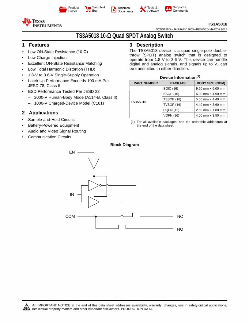
NC COM IN NO EN Product Folder Sample & Buy Technical Documents Tools & Software Support & Community TS3A5018 SCDS189G – JANUARY 2005 – REVISED MARCH 2015 TS3A5018 10-Ω Quad SPDT Analog Switch 1 Features 3 Description The TS3A5018 device is a quad single-pole double- 1• Low ON-State Resistance (10 Ω) throw (SPDT) analog switch that is designed to • Low Charge Injection operate from 1.8 V to 3.6 V. This device can handle • Excellent ON-State Resistance Matching digital and analog signals, and signals up to V + can be transmitted in either direction. • Low Total Harmonic Distortion (THD) • 1.8-V to 3.6-V Single-Supply Operation Device Information (1) • Latch-Up Performance Exceeds 100 mA Per PART NUMBER PACKAGE BODY SIZE (NOM) JESD 78, Class II SOIC (16) 9.90 mm × 6.00 mm • ESD Performance Tested Per JESD 22 SSOP (16) 6.00 mm × 4.90 mm – 2000-V Human-Body Mode (A114-B, Class II) TSSOP (16) 5.00 mm × 4.40 mm TS3A5018 – 1000-V Charged-Device Model (C101) TVSOP (16) 4.40 mm × 3.60 mm UQFN (16) 2.50 mm × 1.80 mm 2 Applications VQFN (16) 4.00 mm × 3.50 mm • Sample-and-Hold Circuits (1) For all available packages, see the orderable addendum at the end of the data sheet. • Battery-Powered Equipment • Audio and Video Signal Routing • Communication Circuits Block Diagram 1 An IMPORTANT NOTICE at the end of this data sheet addresses availability, warranty, changes, use in safety-critical applications, intellectual property matters and other important disclaimers. PRODUCTION DATA.
Transcript of TS3A5018 10-ΩQuad SPDT Analog Switch - farnell.com · TS3A5018 10-ΩQuad SPDT Analog Switch ......
NCCOM
IN
NO
EN
Product
Folder
Sample &Buy
Technical
Documents
Tools &
Software
Support &Community
TS3A5018SCDS189G –JANUARY 2005–REVISED MARCH 2015
TS3A5018 10-Ω Quad SPDT Analog Switch1 Features 3 Description
The TS3A5018 device is a quad single-pole double-1• Low ON-State Resistance (10 Ω)
throw (SPDT) analog switch that is designed to• Low Charge Injection operate from 1.8 V to 3.6 V. This device can handle• Excellent ON-State Resistance Matching digital and analog signals, and signals up to V+ can
be transmitted in either direction.• Low Total Harmonic Distortion (THD)• 1.8-V to 3.6-V Single-Supply Operation Device Information(1)• Latch-Up Performance Exceeds 100 mA Per PART NUMBER PACKAGE BODY SIZE (NOM)
JESD 78, Class IISOIC (16) 9.90 mm × 6.00 mm
• ESD Performance Tested Per JESD 22 SSOP (16) 6.00 mm × 4.90 mm– 2000-V Human-Body Mode (A114-B, Class II) TSSOP (16) 5.00 mm × 4.40 mm
TS3A5018– 1000-V Charged-Device Model (C101) TVSOP (16) 4.40 mm × 3.60 mmUQFN (16) 2.50 mm × 1.80 mm2 ApplicationsVQFN (16) 4.00 mm × 3.50 mm
• Sample-and-Hold Circuits (1) For all available packages, see the orderable addendum atthe end of the data sheet.• Battery-Powered Equipment
• Audio and Video Signal Routing• Communication Circuits
Block Diagram
1
An IMPORTANT NOTICE at the end of this data sheet addresses availability, warranty, changes, use in safety-critical applications,intellectual property matters and other important disclaimers. PRODUCTION DATA.

TS3A5018SCDS189G –JANUARY 2005–REVISED MARCH 2015 www.ti.com
Table of Contents1 Features .................................................................. 1 8 Detailed Description ............................................ 17
8.1 Overview ................................................................. 172 Applications ........................................................... 18.2 Functional Block Diagram (Each Switch)................ 173 Description ............................................................. 18.3 Feature Description................................................. 174 Revision History..................................................... 28.4 Device Functional Modes........................................ 175 Pin Configuration and Functions ......................... 3
9 Application and Implementation ........................ 186 Specifications......................................................... 49.1 Application Information............................................ 186.1 Absolute Maximum Ratings ..................................... 49.2 Typical Application ................................................. 186.2 ESD Ratings ............................................................ 4
10 Power Supply Recommendations ..................... 196.3 Recommended Operating Conditions....................... 411 Layout................................................................... 196.4 Thermal Information .................................................. 4
11.1 Layout Guidelines ................................................. 196.5 Electrical Characteristics for 3.3-V Supply................ 511.2 Layout Example .................................................... 196.6 Electrical Characteristics for 2.5-V Supply ............... 6
12 Device and Documentation Support ................. 206.7 Electrical Characteristics for 2.1-V Supply................ 712.1 Device Support .................................................... 206.8 Electrical Characteristics for 1.8-V Supply................ 712.2 Documentation Support ....................................... 216.9 Switching Characteristics for 3.3-V Supply ............... 812.3 Trademarks ........................................................... 216.10 Switching Characteristics for 2.5-V Supply ............. 812.4 Electrostatic Discharge Caution............................ 216.11 Switching Characteristics for 1.8-V Supply ............. 912.5 Glossary ................................................................ 216.12 Typical Characteristics .......................................... 10
13 Mechanical, Packaging, and Orderable7 Parameter Measurement Information ................ 13Information ........................................................... 21
4 Revision HistoryNOTE: Page numbers for previous revisions may differ from page numbers in the current version.
Changes from Revision F (June 2013) to Revision G Page
• Added Applications, Device Information table, Pin Functions table, ESD Ratings table, Thermal Information table,Typical Characteristics, Feature Description section, Device Functional Modes, Application and Implementationsection, Power Supply Recommendations section, Layout section, Device and Documentation Support section, andMechanical, Packaging, and Orderable Information section. ................................................................................................. 1
• Deleted Ordering Information table. ....................................................................................................................................... 1
2 Submit Documentation Feedback Copyright © 2005–2015, Texas Instruments Incorporated
Product Folder Links: TS3A5018

1
2
3
4
5 6 7 8
9
10
11
12
13141516
NC
1
IN V+
EN
NC4
NO4
COM4
NC3
CO
M2
GN
D
CO
M3
NO
3
NO1
COM1
NC2
NO2
CO
M3
1 16
8 9
2
3
4
5
6
7
15
14
13
12
11
10
EN
NC4
NO4
COM4
NC3
NO3
NC1
NO1
COM1
NC2
NO2
COM2
IN V
GN
D
+Logic
Control
11
107
NC2
1
2
3
4
5
16
15
14
13
12
IN
NC1
NO1
COM1
NC4
EN
V+
NO4
COM4
6
COM2
NO2 NC3
NO3
8GND 9 COM3
TS3A5018www.ti.com SCDS189G –JANUARY 2005–REVISED MARCH 2015
5 Pin Configuration and Functions
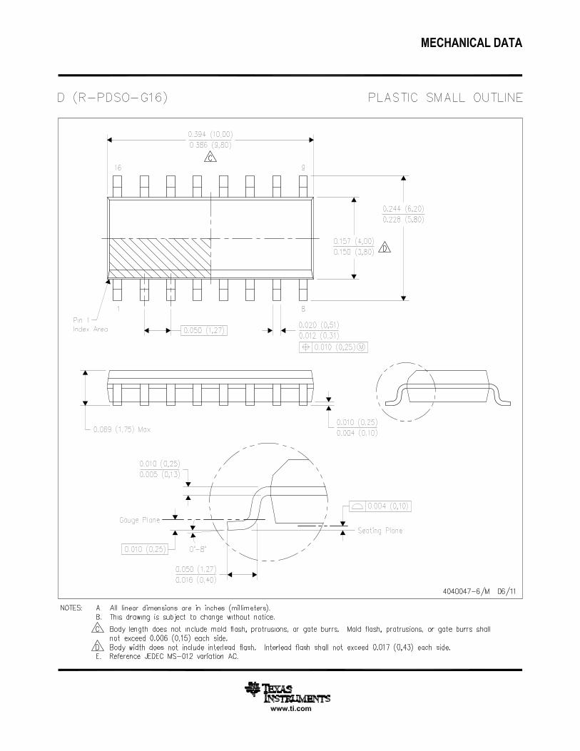
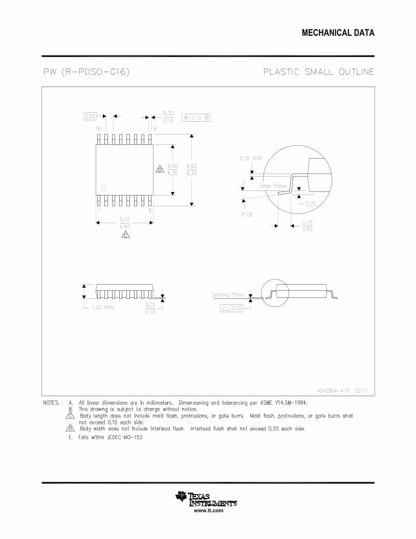
D, DBQ, DGV and PW PackageRGY Package16-Pin SOIC, SSOP, TVSOP and TSSOP16-Pin VQFN(Top View)(Top View)
RSV Package16-Pin UQFN(Top View)
Pin FunctionsPIN
SOIC, SSOP, TYPE DESCRIPTIONNAME TVSOP, VQFN UQFN NO.
NO.COM1 4 2 I/O Common path for switchCOM2 7 5 I/O Common path for switchCOM3 9 7 I/O Common path for switchCOM4 12 10 I/O Common path for switch
EN 15 13 I Active-low switch enable inputGND 8 6 — Ground
IN 1 15 I Switch path selector inputNC1 2 16 I/O Normally closed path for switchNC2 5 3 I/O Normally closed path for switchNC3 11 9 I/O Normally closed path for switchNC4 14 12 I/O Normally closed path for switchNO1 3 1 I/O Normally open path for switchNO2 6 4 I/O Normally open path for switchNO3 10 8 I/O Normally open path for switchNO4 13 11 I/O Normally open path for switchV+ 16 14 — Supply voltage
Copyright © 2005–2015, Texas Instruments Incorporated Submit Documentation Feedback 3
Product Folder Links: TS3A5018

TS3A5018SCDS189G –JANUARY 2005–REVISED MARCH 2015 www.ti.com
6 Specifications
6.1 Absolute Maximum Ratingsover operating free-air temperature range (unless otherwise noted) (1) (2)
MIN MAX UNITV+ Supply voltage (3) –0.5 4.6 VVNC
VNO Analog voltage (3) (4) –0.5 4.6 VVCOM
IK Analog port diode current VNC, VNO, VCOM < 0 –50 mAINC
INO ON-state switch current VNC, VNO, VCOM = 0 to 7 V –64 64 mAICOM
VI Digital input voltage (3) (4) –0.5 4.6 VIIK Digital input clamp current VI < 0 –50 mAI+ Continuous current through V+ –100 100 mAIGND Continuous current through GND –100 100 mATstg Storage temperature –65 150 °C
(1) Stresses beyond those listed under Absolute Maximum Ratings may cause permanent damage to the device. These are stress ratingsonly, and functional operation of the device at these or any other conditions beyond those indicated under Recommended OperatingConditions is not implied. Exposure to absolute-maximum-rated conditions for extended periods may affect device reliability.
(2) The algebraic convention, whereby the most negative value is a minimum and the most positive value is a maximum(3) All voltages are with respect to ground, unless otherwise specified.(4) The input and output voltage ratings may be exceeded if the input and output clamp-current ratings are observed.
6.2 ESD RatingsVALUE UNIT
Human-body model (HBM), per ANSI/ESDA/JEDEC JS-001 (1) ±2000V(ESD) Electrostatic discharge VCharged-device model (CDM), per JEDEC specification JESD22- ±1000
C101 (2)
(1) JEDEC document JEP155 states that 500-V HBM allows safe manufacturing with a standard ESD control process.(2) JEDEC document JEP157 states that 250-V CDM allows safe manufacturing with a standard ESD control process.
6.3 Recommended Operating Conditionsover operating free-air temperature range (unless otherwise noted)
MIN MAX UNITVI/O Switch input and output voltage 0 V+ VV+ Supply voltage 1.65 3.6 VVI Control input voltage 0 3.6 VTA Operating temperature -40 85 °C
6.4 Thermal InformationTS3A5018
D DBQ DGV PW RGY RSVTHERMAL METRIC (1) UNIT(SOIC) (SSOP) (TVSOP) (TSSOP) (VQFN) (UQFN)16 PINS 16 PINS 16 PINS 16 PINS 16 PINS 16 PINS
RθJA Junction-to-ambient thermal resistance 73 90 120 108 51 184 °C/W
(1) For more information about traditional and new thermal metrics, see the IC Package Thermal Metrics application report, SPRA953.
4 Submit Documentation Feedback Copyright © 2005–2015, Texas Instruments Incorporated
Product Folder Links: TS3A5018
TS3A5018www.ti.com SCDS189G –JANUARY 2005–REVISED MARCH 2015
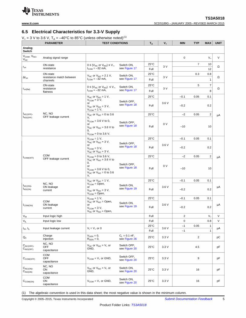
6.5 Electrical Characteristics for 3.3-V SupplyV+ = 3 V to 3.6 V, TA = –40°C to 85°C (unless otherwise noted) (1)
PARAMETER TEST CONDITIONS TA V+ MIN TYP MAX UNIT
AnalogSwitch
VCOM, VNO, Analog signal range 0 V+ VVNC
25°C 7 10ON-state 0 ≤ (VNC or VNO) ≤ V+, Switch ON,ron 3 V Ωresistance ICOM = –32 mA, see Figure 17 Full 12
ON-state 25°C 0.3 0.8VNC or VNO = 2.1 V, Switch ON,Δron resistance match between 3 V ΩICOM = –32 mA, see Figure 17 Full 1channels
ON-state 25°C 5 70 ≤ (VNC or VNO) ≤ V+, Switch ON,ron(flat) resistance 3 V ΩICOM = –32 mA, see Figure 17 Full 8flatness
VNC or VNO = 1 V, 25°C –0.1 0.05 0.1VCOM = 3 V, Switch OFF,or 3.6 Vsee Figure 18 Full –0.2 0.2VNC or VNO = 3 V,VCOM = 1 V,
INC(OFF), NC, NO VNC or VNO = 0 to 3.6 25°C –2 0.05 2 µAINO(OFF) OFF leakage current V,VCOM = 3.6 V to 0, Switch OFF,or 0 Vsee Figure 18 Full –10 10VNC or VNO = 3.6 V to0,VCOM = 0 to 3.6 V,
VCOM = 1 V, 25°C –0.1 0.05 0.1VNC or VNO = 3 V, Switch OFF,or 3.6 Vsee Figure 18 Full –0.2 0.2VCOM = 3 V,VNC or VNO = 3 V,
COM VCOM = 0 to 3.6 V, 25°C –2 0.05 2ICOM(OFF) µAOFF leakage current VNC or VNO = 3.6 V to0, Switch OFF,or 0 Vsee Figure 18 Full –10 10VCOM = 3.6 V to 0,VNC or VNO = 0 to 3.6V,
VNC or VNO = 1 V, 25°C –0.1 0.05 0.1NC, NO VCOM = Open,INC(ON), Switch ON,ON leakage or 3.6 V µAINO(ON) see Figure 19 Full –0.2 0.2current VNC or VNO = 3 V,
VCOM = Open,
VCOM = 1 V, 25°C –0.1 0.05 0.1COM VNC or VNO = Open, Switch ON,ICOM(ON) ON leakage or 3.6 V µAsee Figure 19 Full –0.2 0.2current VCOM = 3 V,
VNC or VNO = Open,
VIH Input logic high Full 2 V+ V
VIL Input logic low Full 0 0.8 V
25°C –1 0.05 1IIH, IIL Input leakage current VI = V+ or 0 3.6 V µA
Full –1 1
Charge VGEN = 0, CL = 0.1 nF,QC 25°C 3.3 V 2 pCinjection RGEN = 0, see Figure 26
NC, NOCNC(OFF), VNC or VNO = V+ or Switch OFF,OFF 25°C 3.3 V 4.5 pFCNO(OFF) GND, see Figure 20capacitance
COM Switch OFF,CCOM(OFF) OFF VCOM = V+ or GND, 25°C 3.3 V 9 pFsee Figure 20capacitance
NC, NOCNC(ON), VNC or VNO = V+ or Switch ON,ON 25°C 3.3 V 16 pFCNO(ON) GND, see Figure 20capacitance
COM Switch ON,CCOM(ON) ON VCOM = V+ or GND, 25°C 3.3 V 16 pFsee Figure 20capacitance
(1) The algebraic convention is used in this data sheet; the most negative value is shown in the minimum column.
Copyright © 2005–2015, Texas Instruments Incorporated Submit Documentation Feedback 5
Product Folder Links: TS3A5018

TS3A5018SCDS189G –JANUARY 2005–REVISED MARCH 2015 www.ti.com
Electrical Characteristics for 3.3-V Supply (continued)V+ = 3 V to 3.6 V, TA = –40°C to 85°C (unless otherwise noted)(1)
PARAMETER TEST CONDITIONS TA V+ MIN TYP MAX UNIT
Digital inputCI VI = V+ or GND, See Figure 20 25°C 3.3 V 3 pFcapacitance
Switch ON,BW Bandwidth RL = 50 Ω, 25°C 3.3 V 300 MHzsee Figure 22
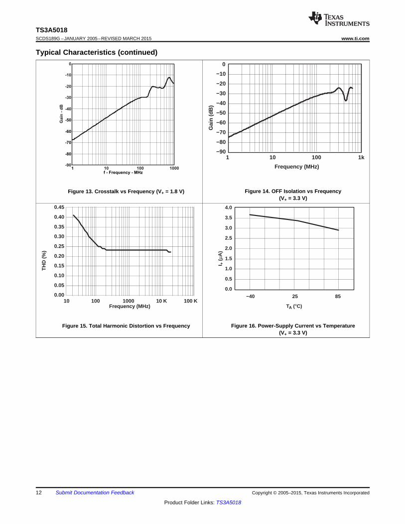
RL = 50 Ω, Switch OFF,OISO OFF isolation 25°C 3.3 V –48 dBf = 10 MHz, see Figure 23
RL = 50 Ω, Switch ON,XTALK Crosstalk 25°C 3.3 V –48 dBf = 10 MHz, see Figure 24
RL = 50 Ω, Switch ON,XTALK(ADJ) Crosstalk adjacent 25°C 3.3 V –81 dBf = 10 MHz, see Figure 25
f = 20 Hz to 20RL = 600 Ω,THD Total harmonic distortion kHz, 25°C 3.3 V 0.21%CL = 50 pF, see Figure 27
25°C 2.5 7I+ Positive supply current VI = V+ or GND, Switch ON or OFF 3.6 V µA
Full 10
6.6 Electrical Characteristics for 2.5-V SupplyV+ = 2.3 V to 2.7 V, TA = –40°C to 85°C (unless otherwise noted) (1)
PARAMETER TEST CONDITIONS TA V+ MIN TYP MAX UNIT
VCOM, VNC, Analog signal range 0 V+ VVNO
25°C 12 20ON-state 0 ≤ (VNC or VNO) ≤ V+, Switch ON,ron 2.3 V Ωresistance ICOM = –24 mA, see Figure 17 Full 22
ON-state 25°C 0.3 1VNC or VNO = 1.6 V, Switch ON,Δron resistance match 2.3 V ΩICOM = –24 mA, see Figure 17 Full 2between channels
ON-state 25°C 14 180 ≤ (VNC or VNO) ≤ V+, Switch ON,ron(flat) resistance 2.3 V ΩICOM = –24 mA, see Figure 17 Full 20flatness
VNC or VNO = 0.5 V, 25°C –0.1 0.05 0.1VCOM = 2.2 V, Switch OFF,or 2.7 Vsee Figure 18 Full –0.2 0.2VNC or VNO = 2.2 V,VCOM = 0.5 V,INC(OFF), NC, NO µAINO(OFF) OFF leakage current VNC or VNO = 0 to 3.6 V, 25°C –2 0.05 2VCOM = 3.6 V to 0, Switch OFF,or 0 Vsee Figure 18 Full –10 10VNC or VNO = 3.6 V to 0,VCOM = 0 to 3.6 V,
VCOM = 0.5 V, 25°C –0.1 0.05 0.1VNC or VNO = 2.2 V, Switch OFF,or 2.7 Vsee Figure 18 Full –0.2 0.2VCOM = 2.2 V,VNC or VNO = 0.5 V,COMICOM(OFF) µAOFF leakage current VCOM = 0 to 3.6 V, 25°C –2 0.05 2VNC or VNO = 3.6 V to 0, Switch OFF,or 0 Vsee Figure 18 Full –10 10VCOM = 3.6 V to 0,VNC or VNO = 0 to 3.6 V,
VNC or VNO = 0.5 V, 25°C –0.1 0.05 0.1NC, NO VCOM = Open,INC(ON), Switch ON,ON leakage or 2.7 V µAINO(ON) see Figure 19 Full –0.2 0.2current VNC or VNO = 2.2 V,
VCOM = Open,
VCOM = 0.5 V, 25°C –0.1 0.05 0.1COM VNC or VNO = Open, Switch ON,ICOM(ON) ON leakage or 2.7 V µAsee Figure 19 Full –0.2 0.2current VCOM = 2.2 V,
VNC or VNO = Open,
VIH Input logic high Full 1.7 V+ V
VIL Input logic low Full 0 0.7 V
(1) The algebraic convention is used in this data sheet; the most negative value is shown in the minimum column.
6 Submit Documentation Feedback Copyright © 2005–2015, Texas Instruments Incorporated
Product Folder Links: TS3A5018

TS3A5018www.ti.com SCDS189G –JANUARY 2005–REVISED MARCH 2015
Electrical Characteristics for 2.5-V Supply (continued)V+ = 2.3 V to 2.7 V, TA = –40°C to 85°C (unless otherwise noted)(1)
PARAMETER TEST CONDITIONS TA V+ MIN TYP MAX UNIT
25°C –0.1 0.05 0.1IIH, IIL Input leakage current VI = V+ or 0 2.7 V µA
Full –1 1
Charge VGEN = 0, CL = 0.1 nF,QC 25°C 2.5 V 1 pCinjection RGEN = 0, see Figure 26
NC, NOCNC(OFF), Switch OFF,OFF VNC or VNO = V+ or GND, 25°C 2.5 V 3 pFCNO(OFF) see Figure 20capacitance
COM Switch OFF,CCOM(OFF) OFF VCOM = V+ or GND, 25°C 2.5 V 9 pFsee Figure 20capacitance
NC, NOCNC(ON), Switch ON,ON VNC or VNO = V+ or GND, 25°C 2.5 V 16 pFCNO(ON) see Figure 20capacitance
COM Switch ON,CCOM(ON) ON VCOM = V+ or GND, 25°C 2.5 V 16 pFsee Figure 20capacitance
Digital inputCI VI = V+ or GND, See Figure 20 25°C 2.5 V 3 pFcapacitance
Switch ON,BW Bandwidth RL = 50 Ω, 25°C 2.5 V 300 MHzsee Figure 22
RL = 50 Ω, Switch OFF,OISO OFF isolation 25°C 2.5 V –48 dBf = 10 MHz, see Figure 23
RL = 50 Ω, Switch ON,XTALK Crosstalk 25°C 2.5 V –48 dBf = 10 MHz, see Figure 24
RL = 50 Ω, Switch ON,XTALK(ADJ) Crosstalk adjacent 25°C 3.3 V –81 dBf = 10 MHz, see Figure 25
Total harmonic RL = 600 Ω, f = 20 Hz to 20 kHz,THD 25°C 2.5 V 0.33%distortion CL = 50 pF, see Figure 27
25°C 2.5 7I+ Positive supply current VI = V+ or GND, Switch ON or OFF 2.7 V µA
Full 10
6.7 Electrical Characteristics for 2.1-V SupplyV+ = 2.00 V to 2.20 V, TA = –40°C to 85°C (unless otherwise noted) (1)
PARAMETER TEST CONDITIONS TA V+ MIN TYP MAX UNITVIH Input logic high Full 1.2 4.3 VVIL Input logic low Full 0 0.5 V
(1) The algebraic convention is used in this data sheet; the most negative value is shown in the minimum column.
6.8 Electrical Characteristics for 1.8-V SupplyV+ = 1.65 V to 1.95 V, TA = –40°C to 85°C (unless otherwise noted) (1)
PARAMETER TEST CONDITIONS TA V+ MIN TYP MAX UNIT
Analog signalVCOM, VNC, VNO 0 V+ Vrange
25°C 5.5 8ON-state 0 ≤ (VNC or VNO) ≤ V+, Switch ON,ron 1.65 V Ωresistance ICOM = –32 mA, see Figure 17 Full 14.55
ON-state 25°C 0.3 1resistance match VNC or VNO = 1.5 V, Switch ON,Δron 1.65 V Ωbetween ICOM = –32 mA, see Figure 17 Full 1.2channels
ON-state 25°C 2.7 5.50 ≤ (VNC or VNO) ≤ V+, Switch ON,ron(flat) resistance 1.65 V ΩICOM = –32 mA, see Figure 17 Full 7.3flatness
(1) The algebraic convention is used in this data sheet; the most negative value is shown in the minimum column.
Copyright © 2005–2015, Texas Instruments Incorporated Submit Documentation Feedback 7
Product Folder Links: TS3A5018

TS3A5018SCDS189G –JANUARY 2005–REVISED MARCH 2015 www.ti.com
Electrical Characteristics for 1.8-V Supply (continued)V+ = 1.65 V to 1.95 V, TA = –40°C to 85°C (unless otherwise noted)(1)
PARAMETER TEST CONDITIONS TA V+ MIN TYP MAX UNIT
VNC or VNO = 0.3 V, 25°C –0.25 0.03 0.25VCOM = 1.65V, Switch OFF,or 1.95 Vsee Figure 18 Full –4.5 4.5VNC or VNO = 1.65V,
NC, NO VCOM = 0.3 V,INC(OFF), OFF leakage µAINO(OFF) VNC or VNO = 1.95 V to 0 V, 25°C –0.4 0.01 0.4currentVCOM = 0 V to 1.95 V, Switch OFF,or 0 Vsee Figure 18 Full –6.5 6.5VNC or VNO = 0 V to 1.95 V,VCOM = 1.95 V to 0 V,
VCOM = 1.65 V, 25°C –0.4 0.02 0.4VNC or VNO = 0.3V, Switch OFF,or 1.95 Vsee Figure 18 Full –0.9 0.9VCOM = 0.3 V,
COM VNC or VNO = 1.65V,ICOM(OFF) OFF leakage µA
VCOM = 0 V to 1.95 V, 25°C –0.4 0.02 0.4currentVNC or VNO = 1.95 V to 0 V, Switch OFF,or 0 Vsee Figure 18 Full –4.5 4.5VCOM = 1.95 V to 0,VNC or VNO = 0 to 1.95 V,
VNC or VNO = 0.3 V, 25°C –2. 0.02 2NC, NO VCOM = Open,INC(ON), Switch ON,ON leakage or 1.95 V µAINO(ON) see Figure 19 Full –2 0.02 2current VNC or VNO = 1.65 V,
VCOM = Open,
VCOM = 0.3 V, 25°C –4.5 4.5COM VNC or VNO = Open, Switch ON,ICOM(ON) ON leakage or 1.95 V µAsee Figure 19 Fullcurrent VCOM = 1.65 V,
VNC or VNO = Open,
VIH Input logic high VI = V+ or GND Full 1.95 V 1 3.6 V
VIL Input logic low Full 1.95 V 0 0.4 V
25°C –0.1 0.01 0.1Input leakageIIH, IIL VI = V+ or 0 1.95 V µAcurrent Full –2.1 2.1
6.9 Switching Characteristics for 3.3-V Supplyover operating free-air temperature range (unless otherwise noted)
PARAMETER TEST CONDITIONS TA V+ MIN TYP MAX UNIT25°C 3.3 V 2.5 3.5 8
VCOM = 2 V, CL = 35 pF,tON Turnon time ns3 V toRL = 300 Ω, see Figure 21 Full 2.5 93.6 V25°C 3.3 V 0.5 2 6.5
VCOM =2 V, CL = 35 pF,tOFF Turnoff time ns3 V toRL = 300 Ω, see Figure 21 Full 0.5 73.6 V
6.10 Switching Characteristics for 2.5-V Supplyover operating free-air temperature range (unless otherwise noted)
PARAMETER TEST CONDITIONS TA V+ MIN TYP MAX UNIT25°C 2.5 V 2.5 5 9.5
VCOM = 1.5 V, CL = 35 pF,tON Turnon time ns2.3 V toRL = 300 Ω, see Figure 21 Full 2.5 10.52.7 V25°C 2.5 V 0.5 3 7.5
VCOM =1.5 V, CL = 35 pF,tOFF Turnoff time ns2.3 V toRL = 300 Ω, see Figure 21 Full 0.5 92.7 V
8 Submit Documentation Feedback Copyright © 2005–2015, Texas Instruments Incorporated
Product Folder Links: TS3A5018

TS3A5018www.ti.com SCDS189G –JANUARY 2005–REVISED MARCH 2015
6.11 Switching Characteristics for 1.8-V Supplyover operating free-air temperature range (unless otherwise noted)
PARAMETER TEST CONDITIONS TA V+ MIN TYP MAX UNIT25°C 1.8 V 14.1 49.3
VCOM = V+, CL = 35 pF, 1.65 VtON Turnon time nsRL = 50 Ω, see Figure 21 Full to 49.3 56.71.95 V
25°C 1.8 V 16.1 26.5VCOM = V+, CL = 35 pF, 1.65 VtOFF Turnoff time nsRL = 50 Ω, see Figure 21 Full to 31.2
1.95 V25°C 1.8 V 5.3 18.4 58
Break-before- VNC = VNO = V+/2, CL = 35 pF, 1.65 VtBBM nsmake time RL = 50 Ω, see Figure 21 Full to 581.95 V
Copyright © 2005–2015, Texas Instruments Incorporated Submit Documentation Feedback 9
Product Folder Links: TS3A5018

0
1
2
3
4
5
0 1 2 3 4
Ch
arg
e In
ject
ion
(pC
)
V+ = 3.3 V
V+ = 2.5 V
VCOM (V) V - VCOM
Ch
arg
e I
nje
cti
on
- p
C
-0.6
-0.5
-0.4
-0.3
-0.2
-0.1
0.0
0.1
0.2
0.3
0.4
0.5
0.6
0.0 0.2 0.4 0.6 0.8 1.0 1.2 1.4 1.6 1.8 2.0
0
5
10
15
20
25
30
35
40
−60 −40 −20 0 20 40 60 80 100Temperature (°C)
Leak
age
Cur
rent
(nA
)
INC_ONINO_ONICOM_ONINC_OFFINO_OFFICOM_OFF
G005
0
10
20
30
40
−60 −40 −20 0 20 40 60 80 100
TA (°C)
Leakag
e C
urr
en
t (n
A)
INC(ON)
INO(ON)
INO(OFF)
ICOM(ON)
ICOM(OFF)
INC(OFF)
0
2
4
6
8
10
0.0 0.5 1.0 1.5 2.0 2.5 3.0 3.5VCOM (V)
r on
85C
25C
–40C
0
2
4
6
8
10
12
14
16
18
0.0 0.5 1.0 1.5 2.0 2.5 3.0 3.5
V+ = 2.5 V
VCOM (V)
r on
(Ω)
V+ = 3.3 V
TA = 25°C
TS3A5018SCDS189G –JANUARY 2005–REVISED MARCH 2015 www.ti.com
6.12 Typical Characteristics
Figure 2. ron vs VCOM (V+ = 2.5 V)Figure 1. ron vs VCOM (V+ = 3.3 V)
Figure 3. Leakage Current vs Temperature (V+ = 3.6 V) Figure 4. Leakage Current vs Temperature (V+ = 1.8 V)
Figure 6. Charge Injection (QC) vs VCOM (V+ = 1.8 V)Figure 5. Charge Injection (QC) vs VCOM
10 Submit Documentation Feedback Copyright © 2005–2015, Texas Instruments Incorporated
Product Folder Links: TS3A5018

f - Frequency - MHz
Ga
in -
dB
-90
-80
-70
-60
-50
-40
-30
-20
-10
0
1 10 100 1000f - Frequency - MHz
Ga
in -
dB
-110
-80
-70
-60
-50
-40
-30
-20
-10
0
1 10 100 1000
-90
-100
−7
−6
−5
−4
−3
−2
−1
0
1 10 100 1K
Gai
n (d
B)
Frequency (MHz)
0
0.2
0.4
0.6
0.8
1
1.2
1.4
1.6
1.8
1.65 1.85 2.05 2.25 2.45 2.65 2.85 3.05 3.25 3.45 3.6V+ (V)
Logi
c Le
vel T
hres
hold
(V
)
VIHVIL
TA = 25°C
G001
0
1
2
3
4
5
6
7
2.0 2.5 3.0 3.5 4.0
V+ (V)
t ON
/tO
FF (n
s)
tON
tOFF
0
1
2
3
4
5
6
7
8
−40 25 85
t ON
/tO
FF (n
s)
TA (C)
tON
tOFF
TS3A5018www.ti.com SCDS189G –JANUARY 2005–REVISED MARCH 2015
Typical Characteristics (continued)
Figure 8. tON and tOFF vs Temperature (V+ = 3.3 V)Figure 7. tON and tOFF vs Supply Voltage
Figure 10. Gain vs Frequency Bandwidth (V+ = 3.3 V)Figure 9. Logic-Level Threshold vs V+
Figure 11. OFF Isolation vs Frequency (V+ = 1.8 V) Figure 12. Crosstalk Adjacent vs Frequency (V+ = 1.8 V)
Copyright © 2005–2015, Texas Instruments Incorporated Submit Documentation Feedback 11
Product Folder Links: TS3A5018
0.00
0.05
0.10
0.15
0.20
0.25
0.30
0.35
0.40
0.45
TH
D (
%)
Frequency (MHz)10 100 100 K1000 10 K
I + (
µA)
0.0
0.5
1.0
1.5
2.0
2.5
3.0
3.5
4.0
−40 25 85
TA (C)
f - Frequency - MHz
Ga
in -
dB
-80
-70
-60
-50
-40
-30
-20
-10
0
1 10 100 1000-90
−90
−80
−70
−60
−50
−40
−30
−20
−10
0
1 10 100 1k
Gai
n (d
B)
Frequency (MHz)
TS3A5018SCDS189G –JANUARY 2005–REVISED MARCH 2015 www.ti.com
Typical Characteristics (continued)
Figure 14. OFF Isolation vs FrequencyFigure 13. Crosstalk vs Frequency (V+ = 1.8 V)(V+ = 3.3 V)
Figure 16. Power-Supply Current vs TemperatureFigure 15. Total Harmonic Distortion vs Frequency(V+ = 3.3 V)
12 Submit Documentation Feedback Copyright © 2005–2015, Texas Instruments Incorporated
Product Folder Links: TS3A5018
Channel ON
ON-State Leakage Current
VI = VIH or VIL
V+
GND
NC
VI
NO
COMVCOM
VNO
VNC
+
+
IN or EN
Channel OFF
VCOM =V+ to 0
OFF-State Leakage Current
and
VI = VIH or VIL
VNC or VNO = 0 to V+
V+
GND
NC
VI
NO
COM VCOM
VNO
VNC
+
+
+
IN or EN
V+
ICOM
ron
VCOM
VNO
or VNC
ICOM
GND
Channel ON
NC
VI
NO
COM VCOM
VI = VIH or VIL
VNO
VNC
IN or EN
+
+
=–
Ω
TS3A5018www.ti.com SCDS189G –JANUARY 2005–REVISED MARCH 2015
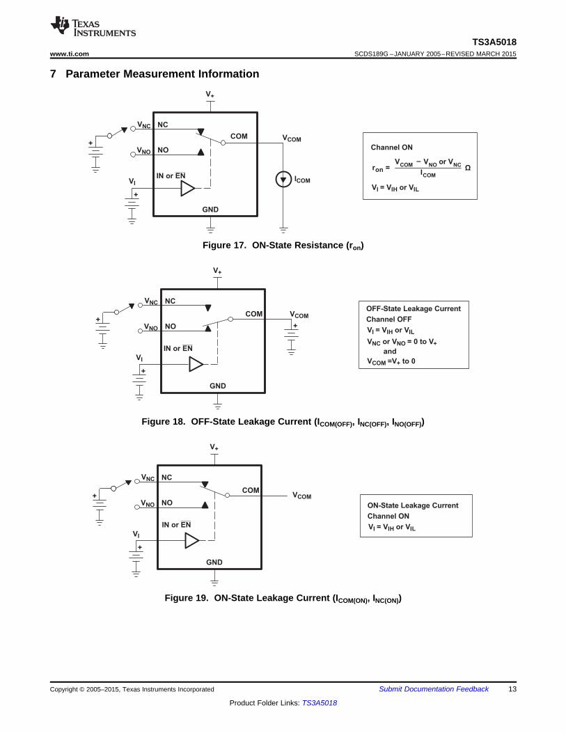
7 Parameter Measurement Information
Figure 17. ON-State Resistance (ron)
Figure 18. OFF-State Leakage Current (ICOM(OFF), INC(OFF), INO(OFF))
Figure 19. ON-State Leakage Current (ICOM(ON), INC(ON))
Copyright © 2005–2015, Texas Instruments Incorporated Submit Documentation Feedback 13
Product Folder Links: TS3A5018

V+
GND
NC
VI
COM
50
50
VNC
VCOM
Channel ON: NC to COM
Network Analyzer Setup
Source Power = 0 dBm
(632-mV P-P at 50- load)
DC Bias = 350 mV
Network Analyzer
Source
Signal
+
VI = V+ or GND
IN or EN
VNO NO
Ω
ΩΩ
CL(2) RL
VCOM
V+
GND
NC or NO VNC or VNO
VI
COM
Logic
Input(1)
300 Ω
RL CL
35 pFtON
TEST
300 Ω 35 pFtOFF
50%
tON tOFF
50%
90% 90%
Logic
Input
(VI)
V+
Switch
Output
(VNC)
0IN or EN
(3)
RL
CL(2)NC or NO
V+
GND
VBIAS
VI
VI = VIH or VIL
VBIAS = V+ or GND
Capacitance is measured at NC,
NO, COM, and IN inputs during
ON and OFF conditions.
Capacitance
Meter
VCOM
VNO
VNC
COM
NO
NC
IN or EN
TS3A5018SCDS189G –JANUARY 2005–REVISED MARCH 2015 www.ti.com
Parameter Measurement Information (continued)
Figure 20. Capacitance (CI, CCOM(OFF), CCOM(ON), CNC(OFF), CNC(ON))
(1) All input pulses are supplied by generators having the following characteristics: PRR ≤ 10 MHz, ZO = 50 Ω, tr < 5 ns,tf < 5 ns.
(2) CL includes probe and jig capacitance.(3) See Electrical Characteristics for VCOM.
Figure 21. Turnon (tON) and Turnoff Time (tOFF)
Figure 22. Bandwidth (BW)
14 Submit Documentation Feedback Copyright © 2005–2015, Texas Instruments Incorporated
Product Folder Links: TS3A5018
NC1
NC2
50
50
COM1Channel ON: NC to COM
Network Analyzer Setup
Source Power = 0 dBm
(632 mV P-P at 50 load)
DC Bias = 350 mV
50
V+
GND
Source
Signal
Network Analyzer
COM2IN or EN
VI
+
VNC1
VNC2
Ω
Ω
Ω
Ω
NC
NO
50
50
VNC
VCOM
Channel ON: NC to COM
Network Analyzer Setup
Source Power = 0 dBm
(632-mV P-P at 50- load)
DC Bias = 350 mV
50
V+
GND
VNO
Source
Signal
Channel OFF: NO to COM
Network Analyzer
VI
+
VI = V+ or GND
IN or EN
Ω
Ω
Ω
Ω
NC
COM
VNC
VCOM
Channel OFF: NC to COM
Network Analyzer Setup
Source Power = 0 dBm
(632-mV P-P at 50- load)
DC Bias = 350 mV
50
V+
GND
50
50
Network Analyzer
Source
Signal
VI
+
VI = V+ or GND
IN or EN
VNO NO
Ω
Ω Ω
TS3A5018www.ti.com SCDS189G –JANUARY 2005–REVISED MARCH 2015
Parameter Measurement Information (continued)
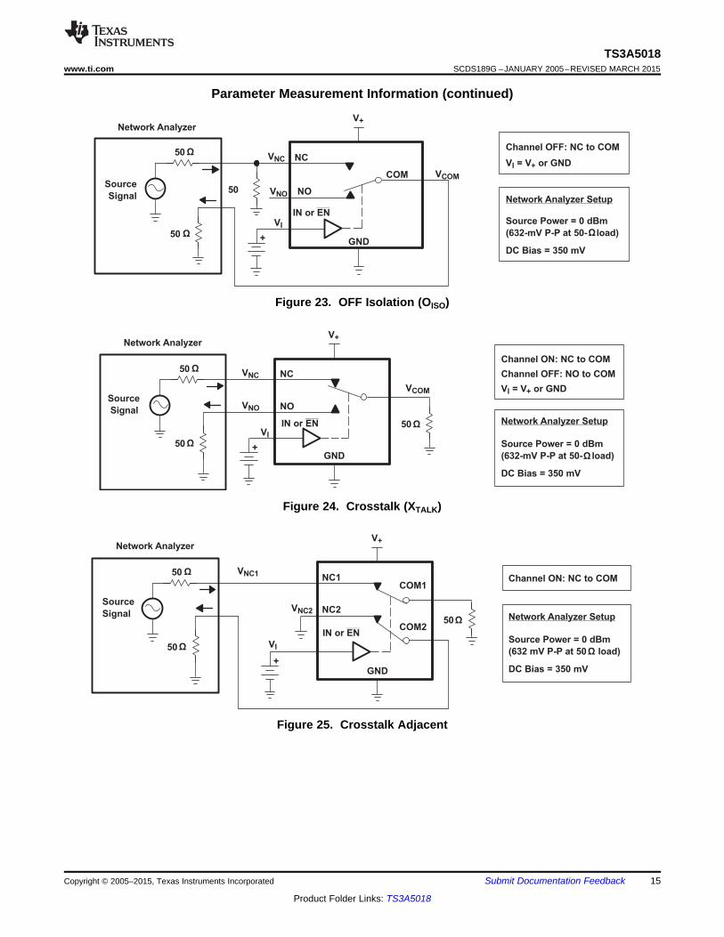
Figure 23. OFF Isolation (OISO)
Figure 24. Crosstalk (XTALK)
Figure 25. Crosstalk Adjacent
Copyright © 2005–2015, Texas Instruments Incorporated Submit Documentation Feedback 15
Product Folder Links: TS3A5018
V+
GND
NC
COM
10 F
CL(1)
RL
V+/2
10 F
IN or ENVI
+
600600
600
Audio Analyzer
Source
Signal
NO
VSOURCE = V+ P-P fSOURCE = 20 Hz to 20 kHz
Channel ON: COM to NC VI = VIH or VIL
Ω
ΩΩ
µ
µ
V+
GND
NC or NORGEN
VI
NC or NO
COM VCOM
CL(1)
OFF
VCOM
ON OFF
ΔVCOMVGEN
+
VI = VIH or VIL
CL = 0.1 nF
VGEN = 0 to V+
RGEN = 0
QC = CL × ΔVCOM
Logic
Input(2)
VIH
VIL
Logic
Input
(VI
IN or EN
)
TS3A5018SCDS189G –JANUARY 2005–REVISED MARCH 2015 www.ti.com
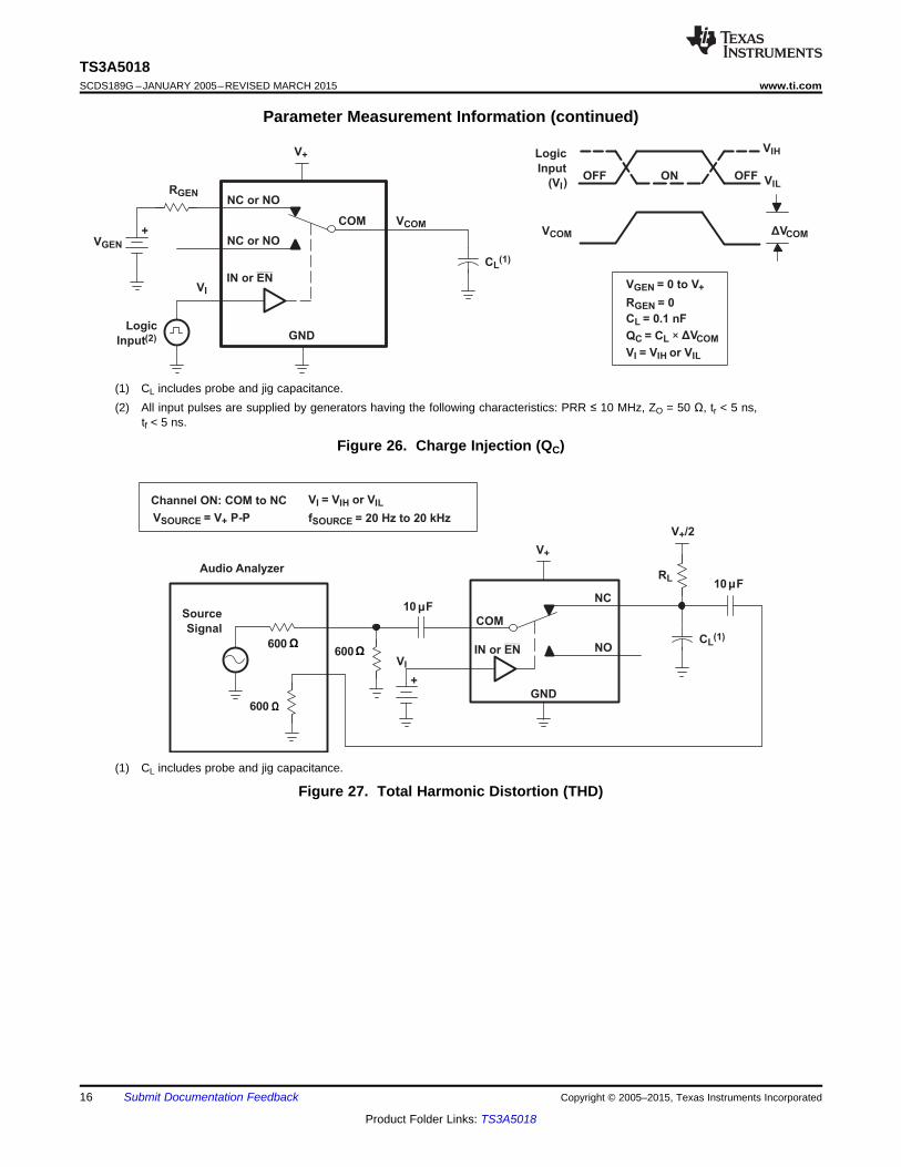
Parameter Measurement Information (continued)
(1) CL includes probe and jig capacitance.(2) All input pulses are supplied by generators having the following characteristics: PRR ≤ 10 MHz, ZO = 50 Ω, tr < 5 ns,
tf < 5 ns.
Figure 26. Charge Injection (QC)
(1) CL includes probe and jig capacitance.
Figure 27. Total Harmonic Distortion (THD)
16 Submit Documentation Feedback Copyright © 2005–2015, Texas Instruments Incorporated
Product Folder Links: TS3A5018
NCCOM
IN
NO
EN
TS3A5018www.ti.com SCDS189G –JANUARY 2005–REVISED MARCH 2015
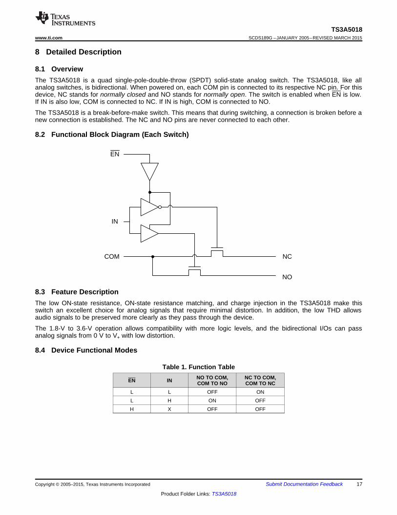
8 Detailed Description
8.1 OverviewThe TS3A5018 is a quad single-pole-double-throw (SPDT) solid-state analog switch. The TS3A5018, like allanalog switches, is bidirectional. When powered on, each COM pin is connected to its respective NC pin. For thisdevice, NC stands for normally closed and NO stands for normally open. The switch is enabled when EN is low.If IN is also low, COM is connected to NC. If IN is high, COM is connected to NO.
The TS3A5018 is a break-before-make switch. This means that during switching, a connection is broken before anew connection is established. The NC and NO pins are never connected to each other.
8.2 Functional Block Diagram (Each Switch)
8.3 Feature DescriptionThe low ON-state resistance, ON-state resistance matching, and charge injection in the TS3A5018 make thisswitch an excellent choice for analog signals that require minimal distortion. In addition, the low THD allowsaudio signals to be preserved more clearly as they pass through the device.
The 1.8-V to 3.6-V operation allows compatibility with more logic levels, and the bidirectional I/Os can passanalog signals from 0 V to V+ with low distortion.
8.4 Device Functional Modes
Table 1. Function TableNO TO COM, NC TO COM,EN IN COM TO NO COM TO NC
L L OFF ONL H ON OFFH X OFF OFF
Copyright © 2005–2015, Texas Instruments Incorporated Submit Documentation Feedback 17
Product Folder Links: TS3A5018

f - Frequency - MHz
Ga
in -
dB
-10
-9
-8
-7
-6
-5
-4
-3
-2
-1
0
1 10 100 1000
C or System
Logic COM1
COM4
NO1
NC1
GND
1.8 V
IN
V+
EN
NO4
NC4
To/From
System
To/From
System
TS3A5018SCDS189G –JANUARY 2005–REVISED MARCH 2015 www.ti.com
9 Application and Implementation
NOTEInformation in the following applications sections is not part of the TI componentspecification, and TI does not warrant its accuracy or completeness. TI’s customers areresponsible for determining suitability of components for their purposes. Customers shouldvalidate and test their design implementation to confirm system functionality.
9.1 Application InformationThe TS3A5018 can be used in a variety of customer systems. The TS3A5018 can be used anywhere multipleanalog or digital signals must be selected to pass across a single line.
9.2 Typical Application
Figure 28. System Schematic for TS3A5018
9.2.1 Design RequirementsIn this particular application, V+ was 1.8 V, although V+ is allowed to be any voltage specified in RecommendedOperating Conditions. A decoupling capacitor is recommended on the V+ pin. See Power SupplyRecommendations for more details.
9.2.2 Detailed Design ProcedureIn this application, EN and IN are, by default, pulled low to GND. Choose these resistor sizes based on thecurrent driving strength of the GPIO, the desired power consumption, and the switching frequency (if applicable).If the GPIO is open-drain, use pullup resistors instead.
9.2.3 Application Curve
Figure 29. Gain vs Frequency Bandwidth (V+ = 1.8 V)
18 Submit Documentation Feedback Copyright © 2005–2015, Texas Instruments Incorporated
Product Folder Links: TS3A5018

WORST BETTER BEST
1W min.
W
2W
TS3A5018www.ti.com SCDS189G –JANUARY 2005–REVISED MARCH 2015
10 Power Supply RecommendationsThe power supply can be any voltage between the minimum and maximum supply voltage rating located in theRecommended Operating Conditions.
Each VCC terminal should have a good bypass capacitor to prevent power disturbance. For devices with a singlesupply, a 0.1-μF bypass capacitor is recommended. If there are multiple pins labeled VCC, then a 0.01-μF or0.022-μF capacitor is recommended for each VCC because the VCC pins will be tied together internally. Fordevices with dual supply pins operating at different voltages, for example VCC and VDD, a 0.1-µF bypasscapacitor is recommended for each supply pin. It is acceptable to parallel multiple bypass capacitors to rejectdifferent frequencies of noise. 0.1-μF and 1-μF capacitors are commonly used in parallel. The bypass capacitorshould be installed as close to the power terminal as possible for best results.
11 Layout
11.1 Layout GuidelinesReflections and matching are closely related to loop antenna theory, but different enough to warrant their owndiscussion. When a PCB trace turns a corner at a 90° angle, a reflection can occur. This is primarily due to thechange of width of the trace. At the apex of the turn, the trace width is increased to 1.414 times its width. Thisupsets the transmission line characteristics, especially the distributed capacitance and self–inductance of thetrace — resulting in the reflection. It is a given that not all PCB traces can be straight, and so they will have toturn corners. Below figure shows progressively better techniques of rounding corners. Only the last examplemaintains constant trace width and minimizes reflections.
Unused switch I/Os, such as NO, NC, and COM, can be left floating or tied to GND. However, the IN and ENpins must be driven high or low. Due to partial transistor turnon when control inputs are at threshold levels,floating control inputs can cause increased ICC or unknown switch selection states.
11.2 Layout Example
Figure 30. Trace Example
Copyright © 2005–2015, Texas Instruments Incorporated Submit Documentation Feedback 19
Product Folder Links: TS3A5018

TS3A5018SCDS189G –JANUARY 2005–REVISED MARCH 2015 www.ti.com
12 Device and Documentation Support
12.1 Device Support
12.1.1 Device Nomenclature
Table 2. Parameter DescriptionSYMBOL DESCRIPTION
VCOM Voltage at COMVNC Voltage at NCVNO Voltage at NOron Resistance between COM and NC or NO ports when the channel is ONΔron Difference of ron between channels in a specific device
ron(flat) Difference between the maximum and minimum value of ron in a channel over the specified range of conditionsINC(OFF) Leakage current measured at the NC port, with the corresponding channel (NC to COM) in the OFF state
Leakage current measured at the NC port, with the corresponding channel (NC to COM) in the ON state and the outputINC(ON) (COM) openINO(OFF) Leakage current measured at the NO port, with the corresponding channel (NO to COM) in the OFF state
Leakage current measured at the NO port, with the corresponding channel (NO to COM) in the ON state and the outputINO(ON) (COM) openICOM(OFF) Leakage current measured at the COM port, with the corresponding channel (COM to NC or NO) in the OFF state
Leakage current measured at the COM port, with the corresponding channel (COM to NC or NO) in the ON state and theICOM(ON) output (NC or NO) openVIH Minimum input voltage for logic high for the control input (IN, EN)VIL Maximum input voltage for logic low for the control input (IN, EN)VI Voltage at the control input (IN, EN)
IIH, IIL Leakage current measured at the control input (IN, EN)Turnon time for the switch. This parameter is measured under the specified range of conditions and by the propagationtON delay between the digital control (IN) signal and analog output NC or NO) signal when the switch is turning ON.Turnoff time for the switch. This parameter is measured under the specified range of conditions and by the propagationtOFF delay between the digital control (IN) signal and analog output (NC or NO) signal when the switch is turning OFF.Charge injection is a measurement of unwanted signal coupling from the control (IN) input to the analog (NC or NO)
QC output. This is measured in coulomb (C) and measured by the total charge induced due to switching of the control input.Charge injection, QC = CL × ΔVCOM, CL is the load capacitance and ΔVCOM is the change in analog output voltage.
CNC(OFF) Capacitance at the NC port when the corresponding channel (NC to COM) is OFFCNC(ON) Capacitance at the NC port when the corresponding channel (NC to COM) is ONCNO(OFF) Capacitance at the NC port when the corresponding channel (NO to COM) is OFFCNO(ON) Capacitance at the NC port when the corresponding channel (NO to COM) is ON
CCOM(OFF) Capacitance at the COM port when the corresponding channel (COM to NC) is OFFCCOM(ON) Capacitance at the COM port when the corresponding channel (COM to NC) is ON
CI Capacitance of control input (IN, EN)OFF isolation of the switch is a measurement of OFF-state switch impedance. This is measured in dB in a specificOISO frequency, with the corresponding channel (NC to COM) in the OFF state.Crosstalk is a measurement of unwanted signal coupling from an ON channel to an OFF channel (NC1 to NO1). Adjacent
XTALK crosstalk is a measure of unwanted signal coupling from an ON channel to an adjacent ON channel (NC1 to NC2) .This ismeasured in a specific frequency and in dB.
BW Bandwidth of the switch. This is the frequency in which the gain of an ON channel is –3 dB below the DC gain.Total harmonic distortion describes the signal distortion caused by the analog switch. This is defined as the ratio of root
THD mean square (RMS) value of the second, third, and higher harmonic to the absolute magnitude of the fundamentalharmonic.
I+ Static power-supply current with the control (IN) pin at V+ or GND
20 Submit Documentation Feedback Copyright © 2005–2015, Texas Instruments Incorporated
Product Folder Links: TS3A5018

TS3A5018www.ti.com SCDS189G –JANUARY 2005–REVISED MARCH 2015
12.2 Documentation Support
12.2.1 Related DocumentationFor related documentation, see the following:• Implications of Slow or Floating CMOS Inputs, SCBA004
12.3 TrademarksAll trademarks are the property of their respective owners.
12.4 Electrostatic Discharge CautionThese devices have limited built-in ESD protection. The leads should be shorted together or the device placed in conductive foamduring storage or handling to prevent electrostatic damage to the MOS gates.
12.5 GlossarySLYZ022 — TI Glossary.
This glossary lists and explains terms, acronyms, and definitions.
13 Mechanical, Packaging, and Orderable InformationThe following pages include mechanical, packaging, and orderable information. This information is the mostcurrent data available for the designated devices. This data is subject to change without notice and revision ofthis document. For browser-based versions of this data sheet, refer to the left-hand navigation.
Copyright © 2005–2015, Texas Instruments Incorporated Submit Documentation Feedback 21
Product Folder Links: TS3A5018

PACKAGE OPTION ADDENDUM
www.ti.com 10-Jun-2014
Addendum-Page 1
PACKAGING INFORMATION
Orderable Device Status(1)
Package Type PackageDrawing
Pins PackageQty
Eco Plan(2)
Lead/Ball Finish(6)
MSL Peak Temp(3)
Op Temp (°C) Device Marking(4/5)
Samples
TS3A5018D ACTIVE SOIC D 16 40 Green (RoHS& no Sb/Br)
CU NIPDAU Level-1-260C-UNLIM -40 to 85 TS3A5018
TS3A5018DBQR ACTIVE SSOP DBQ 16 2500 Green (RoHS& no Sb/Br)
CU NIPDAU Level-2-260C-1 YEAR -40 to 85 YA018
TS3A5018DBQRE4 ACTIVE SSOP DBQ 16 2500 Green (RoHS& no Sb/Br)
CU NIPDAU Level-2-260C-1 YEAR -40 to 85 YA018
TS3A5018DBQRG4 ACTIVE SSOP DBQ 16 2500 Green (RoHS& no Sb/Br)
CU NIPDAU Level-2-260C-1 YEAR -40 to 85 YA018
TS3A5018DE4 ACTIVE SOIC D 16 40 Green (RoHS& no Sb/Br)
CU NIPDAU Level-1-260C-UNLIM -40 to 85 TS3A5018
TS3A5018DGVR ACTIVE TVSOP DGV 16 2000 Green (RoHS& no Sb/Br)
CU NIPDAU Level-1-260C-UNLIM -40 to 85 YA018
TS3A5018DR ACTIVE SOIC D 16 2500 Green (RoHS& no Sb/Br)
CU NIPDAU Level-1-260C-UNLIM -40 to 85 TS3A5018
TS3A5018DRE4 ACTIVE SOIC D 16 2500 Green (RoHS& no Sb/Br)
CU NIPDAU Level-1-260C-UNLIM -40 to 85 TS3A5018
TS3A5018PW ACTIVE TSSOP PW 16 90 Green (RoHS& no Sb/Br)
CU NIPDAU Level-1-260C-UNLIM -40 to 85 YA018
TS3A5018PWG4 ACTIVE TSSOP PW 16 90 Green (RoHS& no Sb/Br)
CU NIPDAU Level-1-260C-UNLIM -40 to 85 YA018
TS3A5018PWR ACTIVE TSSOP PW 16 2000 Green (RoHS& no Sb/Br)
CU NIPDAU Level-1-260C-UNLIM -40 to 85 YA018
TS3A5018PWRE4 ACTIVE TSSOP PW 16 2000 Green (RoHS& no Sb/Br)
CU NIPDAU Level-1-260C-UNLIM -40 to 85 YA018
TS3A5018RGYR ACTIVE VQFN RGY 16 3000 Green (RoHS& no Sb/Br)
CU NIPDAU Level-2-260C-1 YEAR -40 to 85 YA018
TS3A5018RGYRG4 ACTIVE VQFN RGY 16 3000 Green (RoHS& no Sb/Br)
CU NIPDAU Level-2-260C-1 YEAR -40 to 85 YA018
TS3A5018RSVR ACTIVE UQFN RSV 16 3000 Green (RoHS& no Sb/Br)
CU NIPDAU |CU NIPDAUAG
Level-1-260C-UNLIM -40 to 85 ZUN
(1) The marketing status values are defined as follows:ACTIVE: Product device recommended for new designs.LIFEBUY: TI has announced that the device will be discontinued, and a lifetime-buy period is in effect.NRND: Not recommended for new designs. Device is in production to support existing customers, but TI does not recommend using this part in a new design.
PACKAGE OPTION ADDENDUM
www.ti.com 10-Jun-2014
Addendum-Page 2
PREVIEW: Device has been announced but is not in production. Samples may or may not be available.OBSOLETE: TI has discontinued the production of the device.
(2) Eco Plan - The planned eco-friendly classification: Pb-Free (RoHS), Pb-Free (RoHS Exempt), or Green (RoHS & no Sb/Br) - please check http://www.ti.com/productcontent for the latest availabilityinformation and additional product content details.TBD: The Pb-Free/Green conversion plan has not been defined.Pb-Free (RoHS): TI's terms "Lead-Free" or "Pb-Free" mean semiconductor products that are compatible with the current RoHS requirements for all 6 substances, including the requirement thatlead not exceed 0.1% by weight in homogeneous materials. Where designed to be soldered at high temperatures, TI Pb-Free products are suitable for use in specified lead-free processes.Pb-Free (RoHS Exempt): This component has a RoHS exemption for either 1) lead-based flip-chip solder bumps used between the die and package, or 2) lead-based die adhesive used betweenthe die and leadframe. The component is otherwise considered Pb-Free (RoHS compatible) as defined above.Green (RoHS & no Sb/Br): TI defines "Green" to mean Pb-Free (RoHS compatible), and free of Bromine (Br) and Antimony (Sb) based flame retardants (Br or Sb do not exceed 0.1% by weightin homogeneous material)
(3) MSL, Peak Temp. - The Moisture Sensitivity Level rating according to the JEDEC industry standard classifications, and peak solder temperature.
(4) There may be additional marking, which relates to the logo, the lot trace code information, or the environmental category on the device.
(5) Multiple Device Markings will be inside parentheses. Only one Device Marking contained in parentheses and separated by a "~" will appear on a device. If a line is indented then it is a continuationof the previous line and the two combined represent the entire Device Marking for that device.
(6) Lead/Ball Finish - Orderable Devices may have multiple material finish options. Finish options are separated by a vertical ruled line. Lead/Ball Finish values may wrap to two lines if the finishvalue exceeds the maximum column width.
Important Information and Disclaimer:The information provided on this page represents TI's knowledge and belief as of the date that it is provided. TI bases its knowledge and belief on informationprovided by third parties, and makes no representation or warranty as to the accuracy of such information. Efforts are underway to better integrate information from third parties. TI has taken andcontinues to take reasonable steps to provide representative and accurate information but may not have conducted destructive testing or chemical analysis on incoming materials and chemicals.TI and TI suppliers consider certain information to be proprietary, and thus CAS numbers and other limited information may not be available for release.
In no event shall TI's liability arising out of such information exceed the total purchase price of the TI part(s) at issue in this document sold by TI to Customer on an annual basis.

TAPE AND REEL INFORMATION
*All dimensions are nominal
Device PackageType
PackageDrawing
Pins SPQ ReelDiameter
(mm)
ReelWidth
W1 (mm)
A0(mm)
B0(mm)
K0(mm)
P1(mm)
W(mm)
Pin1Quadrant
TS3A5018DGVR TVSOP DGV 16 2000 330.0 12.4 6.8 4.0 1.6 8.0 12.0 Q1
TS3A5018DR SOIC D 16 2500 330.0 16.4 6.5 10.3 2.1 8.0 16.0 Q1
TS3A5018PWR TSSOP PW 16 2000 330.0 12.4 6.9 5.6 1.6 8.0 12.0 Q1
TS3A5018RGYR VQFN RGY 16 3000 330.0 12.4 3.8 4.3 1.5 8.0 12.0 Q1
TS3A5018RSVR UQFN RSV 16 3000 180.0 12.4 2.1 2.9 0.75 4.0 12.0 Q1
TS3A5018RSVR UQFN RSV 16 3000 180.0 13.2 2.1 2.9 0.75 4.0 12.0 Q1
TS3A5018RSVR UQFN RSV 16 3000 177.8 12.4 2.0 2.8 0.7 4.0 12.0 Q1
PACKAGE MATERIALS INFORMATION
www.ti.com 18-Aug-2014
Pack Materials-Page 1

*All dimensions are nominal
Device Package Type Package Drawing Pins SPQ Length (mm) Width (mm) Height (mm)
TS3A5018DGVR TVSOP DGV 16 2000 367.0 367.0 35.0
TS3A5018DR SOIC D 16 2500 333.2 345.9 28.6
TS3A5018PWR TSSOP PW 16 2000 367.0 367.0 35.0
TS3A5018RGYR VQFN RGY 16 3000 355.0 350.0 50.0
TS3A5018RSVR UQFN RSV 16 3000 203.0 203.0 35.0
TS3A5018RSVR UQFN RSV 16 3000 184.0 184.0 19.0
TS3A5018RSVR UQFN RSV 16 3000 202.0 201.0 28.0
PACKAGE MATERIALS INFORMATION
www.ti.com 18-Aug-2014
Pack Materials-Page 2


IMPORTANT NOTICE
Texas Instruments Incorporated and its subsidiaries (TI) reserve the right to make corrections, enhancements, improvements and otherchanges to its semiconductor products and services per JESD46, latest issue, and to discontinue any product or service per JESD48, latestissue. Buyers should obtain the latest relevant information before placing orders and should verify that such information is current andcomplete. All semiconductor products (also referred to herein as “components”) are sold subject to TI’s terms and conditions of salesupplied at the time of order acknowledgment.TI warrants performance of its components to the specifications applicable at the time of sale, in accordance with the warranty in TI’s termsand conditions of sale of semiconductor products. Testing and other quality control techniques are used to the extent TI deems necessaryto support this warranty. Except where mandated by applicable law, testing of all parameters of each component is not necessarilyperformed.TI assumes no liability for applications assistance or the design of Buyers’ products. Buyers are responsible for their products andapplications using TI components. To minimize the risks associated with Buyers’ products and applications, Buyers should provideadequate design and operating safeguards.TI does not warrant or represent that any license, either express or implied, is granted under any patent right, copyright, mask work right, orother intellectual property right relating to any combination, machine, or process in which TI components or services are used. Informationpublished by TI regarding third-party products or services does not constitute a license to use such products or services or a warranty orendorsement thereof. Use of such information may require a license from a third party under the patents or other intellectual property of thethird party, or a license from TI under the patents or other intellectual property of TI.Reproduction of significant portions of TI information in TI data books or data sheets is permissible only if reproduction is without alterationand is accompanied by all associated warranties, conditions, limitations, and notices. TI is not responsible or liable for such altereddocumentation. Information of third parties may be subject to additional restrictions.Resale of TI components or services with statements different from or beyond the parameters stated by TI for that component or servicevoids all express and any implied warranties for the associated TI component or service and is an unfair and deceptive business practice.TI is not responsible or liable for any such statements.Buyer acknowledges and agrees that it is solely responsible for compliance with all legal, regulatory and safety-related requirementsconcerning its products, and any use of TI components in its applications, notwithstanding any applications-related information or supportthat may be provided by TI. Buyer represents and agrees that it has all the necessary expertise to create and implement safeguards whichanticipate dangerous consequences of failures, monitor failures and their consequences, lessen the likelihood of failures that might causeharm and take appropriate remedial actions. Buyer will fully indemnify TI and its representatives against any damages arising out of the useof any TI components in safety-critical applications.In some cases, TI components may be promoted specifically to facilitate safety-related applications. With such components, TI’s goal is tohelp enable customers to design and create their own end-product solutions that meet applicable functional safety standards andrequirements. Nonetheless, such components are subject to these terms.No TI components are authorized for use in FDA Class III (or similar life-critical medical equipment) unless authorized officers of the partieshave executed a special agreement specifically governing such use.Only those TI components which TI has specifically designated as military grade or “enhanced plastic” are designed and intended for use inmilitary/aerospace applications or environments. Buyer acknowledges and agrees that any military or aerospace use of TI componentswhich have not been so designated is solely at the Buyer's risk, and that Buyer is solely responsible for compliance with all legal andregulatory requirements in connection with such use.TI has specifically designated certain components as meeting ISO/TS16949 requirements, mainly for automotive use. In any case of use ofnon-designated products, TI will not be responsible for any failure to meet ISO/TS16949.
Products ApplicationsAudio www.ti.com/audio Automotive and Transportation www.ti.com/automotiveAmplifiers amplifier.ti.com Communications and Telecom www.ti.com/communicationsData Converters dataconverter.ti.com Computers and Peripherals www.ti.com/computersDLP® Products www.dlp.com Consumer Electronics www.ti.com/consumer-appsDSP dsp.ti.com Energy and Lighting www.ti.com/energyClocks and Timers www.ti.com/clocks Industrial www.ti.com/industrialInterface interface.ti.com Medical www.ti.com/medicalLogic logic.ti.com Security www.ti.com/securityPower Mgmt power.ti.com Space, Avionics and Defense www.ti.com/space-avionics-defenseMicrocontrollers microcontroller.ti.com Video and Imaging www.ti.com/videoRFID www.ti-rfid.comOMAP Applications Processors www.ti.com/omap TI E2E Community e2e.ti.comWireless Connectivity www.ti.com/wirelessconnectivity
Mailing Address: Texas Instruments, Post Office Box 655303, Dallas, Texas 75265Copyright © 2015, Texas Instruments Incorporated