ISL8203M Datasheet - Intersil.com FN8661Rev 4.00 Page 6 of 18 May 12, 2016 DYNAMIC CHARACTERISTICS...
18
FN8661 Rev 4.00 Page 1 of 18 May 12, 2016 FN8661 Rev 4.00 May 12, 2016 ISL8203M Dual 3A/Single 6A Step-Down DC/DC Power Module DATASHEET The ISL8203M is an integrated step-down power module rated for dual 3A output current or 6A current sharing operation. Optimized for generating low output voltages down to 0.8V, the ISL8203M is ideal for any low power low voltage applications. The supply voltage range is from 2.85V to 6V. The two channels are 180° out-of-phase for input RMS current and EMI reduction. Each channel is capable of 3A output current. They can be combined to form a single 6A output in current sharing mode. While in current sharing mode, the interleaving of the two channels reduces input and output voltage ripple. The ISL8203M offers an independent Power-Good (PG) signal for each channel. When shut down, the ISL8203M discharges the output capacitor. Other features include internal digital soft-start, enable for power sequence, overcurrent protection and over-temperature protection. The ISL8203M integrates a PWM controller, synchronous switching MOSFETs, inductors and passive components to maximize efficiency and minimize external component count. The ISL8203M is available in a thermally-enhanced, compact QFN package. Features • Dual 3A and single 6A switching power supply • High efficiency, up to 95% • Input voltage range: 2.85V to 6V • Output voltage range: 0.8V to 5V • Internal digital soft-start: 1.5ms • External synchronization up to 4MHz • Compact size: 9.0mmx6.5mmx1.83mm • Peak current limiting and hiccup mode short-circuit protection • Overcurrent protection Applications • μC/μP, FPGA and DSP power • Plug-in DC/DC modules for routers and switchers • Test and measurement systems • Barcode reader Related Literature • AN1941 , “ISL8203MEVAL2Z Evaluation Board User Guide” FIGURE 1. TYPICAL APPLICATION CIRCUIT - DUAL 3A FIGURE 2. SMALL FOOTPRINT PACKAGE WITH LOW PROFILE ISL8203M VOUT1 FB1 SGND VOUT2 FB2 SGND VIN2 VDD EN1 SYNC EN2 PGND OUTPUT1 1.5V/3A VIN1 100k 113k 80.6k SS 100k 1800pF 1800pF OUTPUT2 1.8V/3A 2x22μF INPUT 2.85V TO 6V 3x22μF 3x22μF 9mm 6.5mm 1.83mm
-
Upload
nguyenhanh -
Category
Documents
-
view
216 -
download
3
Transcript of ISL8203M Datasheet - Intersil.com FN8661Rev 4.00 Page 6 of 18 May 12, 2016 DYNAMIC CHARACTERISTICS...
FN8661Rev 4.00
May 12, 2016
ISL8203MDual 3A/Single 6A Step-Down DC/DC Power Module
DATASHEET
The ISL8203M is an integrated step-down power module rated for dual 3A output current or 6A current sharing operation. Optimized for generating low output voltages down to 0.8V, the ISL8203M is ideal for any low power low voltage applications. The supply voltage range is from 2.85V to 6V. The two channels are 180° out-of-phase for input RMS current and EMI reduction. Each channel is capable of 3A output current. They can be combined to form a single 6A output in current sharing mode. While in current sharing mode, the interleaving of the two channels reduces input and output voltage ripple.
The ISL8203M offers an independent Power-Good (PG) signal for each channel. When shut down, the ISL8203M discharges the output capacitor. Other features include internal digital soft-start, enable for power sequence, overcurrent protection and over-temperature protection.
The ISL8203M integrates a PWM controller, synchronous switching MOSFETs, inductors and passive components to maximize efficiency and minimize external component count. The ISL8203M is available in a thermally-enhanced, compact QFN package.
Features• Dual 3A and single 6A switching power supply
• High efficiency, up to 95%
• Input voltage range: 2.85V to 6V
• Output voltage range: 0.8V to 5V
• Internal digital soft-start: 1.5ms
• External synchronization up to 4MHz
• Compact size: 9.0mmx6.5mmx1.83mm
• Peak current limiting and hiccup mode short-circuit protection
• Overcurrent protection
Applications• µC/µP, FPGA and DSP power
• Plug-in DC/DC modules for routers and switchers
• Test and measurement systems
• Barcode reader
Related Literature• AN1941, “ISL8203MEVAL2Z Evaluation Board User Guide”
FIGURE 1. TYPICAL APPLICATION CIRCUIT - DUAL 3A FIGURE 2. SMALL FOOTPRINT PACKAGE WITH LOW PROFILE
ISL8203M
VOUT1
FB1
SGND
VOUT2
FB2
SGND
VIN2
VDD
EN1
SYNC
EN2
PGND
OUTPUT1 1.5V/3A
VIN1100k
113k
80.6k
SS
100k
1800pF
1800pF
OUTPUT2 1.8V/3A
2x22µF
INPUT2.85V TO 6V
3x22µF
3x22µF9mm
6.5mm
1.83mm
FN8661 Rev 4.00 Page 1 of 18May 12, 2016
ISL8203M
FIGURE 3. INTERNAL BLOCK DIAGRAM
SW1
+CSA1
+
+
+SLOPECOMP
SOFT-START
0.8VEAMP
COMP
PWMLOGIC
CONTROLLERPROTECTION
DRIVERFB1
PG1 SYNC
SHUTDOWN
VIN1
PGND
OSCILLATOR
BANDGAPREFEREN CE
EN1
SHUTDOWN
1msDELAY
SGN D
3pF
1.6k
+
+0.8V
EAMP
COMP
FB2
PG2
EN2
SGN D
THERMALSHUTDOWN
SHUTDOWN
COMP
1M
VIN1
OCP THRESHOLD LOGIC
SS
SS
+
CSA2
PWMLOGIC
CONTROLLERPROTECTION
DRIVER
SHUTDOWN
+SLOPECOMP
BANDGAPREFEREN CE
SHUTDOWN
1msDELAY
VIN2
SW2
PGND
VIN2
VOUT1
VOUT2
SOFT-START
1μH
1μH
1.6k
RC NETWORK
RC NETWORK
PGOOD COMPARATORS
PGOOD COMPARATORS
3pF
1μF
1μF
FN8661 Rev 4.00 Page 2 of 18May 12, 2016
ISL8203M
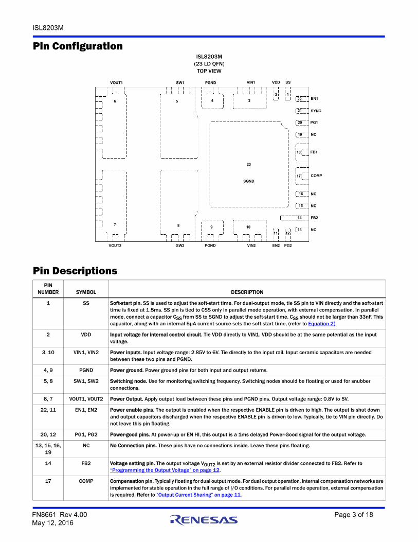
Pin ConfigurationISL8203M
(23 LD QFN)TOP VIEW
VDD SS
123456
7 8 9 1011 12
13
14
15
16
17
18
19
20
21
22
23
VIN1PGNDSW1VOUT1
VOUT2 SW2 PGND VIN2 EN2 PG2
NC
FB2
NC
NC
COMP
FB1
NC
PG1
SYNC
EN1
SGND
Pin DescriptionsPIN
NUMBER SYMBOL DESCRIPTION
1 SS Soft-start pin. SS is used to adjust the soft-start time. For dual-output mode, tie SS pin to VIN directly and the soft-start time is fixed at 1.5ms. SS pin is tied to CSS only in parallel mode operation, with external compensation. In parallel mode, connect a capacitor CSS from SS to SGND to adjust the soft-start time. CSS should not be larger than 33nF. This capacitor, along with an internal 5µA current source sets the soft-start time, (refer to Equation 2).
2 VDD Input voltage for internal control circuit. Tie VDD directly to VIN1. VDD should be at the same potential as the input voltage.
3, 10 VIN1, VIN2 Power inputs. Input voltage range: 2.85V to 6V. Tie directly to the input rail. Input ceramic capacitors are needed between these two pins and PGND.
4, 9 PGND Power ground. Power ground pins for both input and output returns.
5, 8 SW1, SW2 Switching node. Use for monitoring switching frequency. Switching nodes should be floating or used for snubber connections.
6, 7 VOUT1, VOUT2 Power Output. Apply output load between these pins and PGND pins. Output voltage range: 0.8V to 5V.
22, 11 EN1, EN2 Power enable pins. The output is enabled when the respective ENABLE pin is driven to high. The output is shut down and output capacitors discharged when the respective ENABLE pin is driven to low. Typically, tie to VIN pin directly. Do not leave this pin floating.
20, 12 PG1, PG2 Power-good pins. At power-up or EN HI, this output is a 1ms delayed Power-Good signal for the output voltage.
13, 15, 16, 19
NC No Connection pins. These pins have no connections inside. Leave these pins floating.
14 FB2 Voltage setting pin. The output voltage VOUT2 is set by an external resistor divider connected to FB2. Refer to “Programming the Output Voltage” on page 12.
17 COMP Compensation pin. Typically floating for dual output mode. For dual output operation, internal compensation networks are implemented for stable operation in the full range of I/O conditions. For parallel mode operation, external compensation is required. Refer to “Output Current Sharing” on page 11.
FN8661 Rev 4.00 Page 3 of 18May 12, 2016
ISL8203M
18 FB1 Voltage setting pin. The output voltage VOUT1 is set by an external resistor divider connected to FB1. Refer to “Programming the Output Voltage” on page 12.
21 SYNC Synchronization pin. Connect to logic high or input voltage VIN for non-use. Connect to an external function generator for external synchronization. Negative edge trigger. Do not leave this pin floating. Do not tie this pin low (or to PGND).
23 SGND Control signal ground. Connect to PGND under the module on the top layer. Make sure to have only two connect locations between SGND and PGND to avoid noise coupling. See “PCB Layout Recommendation” on page 14.
Pin Descriptions (Continued)
PIN NUMBER SYMBOL DESCRIPTION
Ordering InformationPART NUMBER (Notes 1 2, 3)
PARTMARKING
TEMP. RANGE(°C)
PACKAGE(RoHS Compliant)
PKG.DWG. #
ISL8203MIRZ ISL8203M -40 to +85 23 Ld QFN L23.6.5x9
ISL8203MEVAL2Z Evaluation Board
NOTES:
1. Add “-T” suffix for 1k unit or “-T7A” suffix for 250 unit tape and reel options. Please refer to TB347 for details on reel specifications.
2. These Intersil Pb-free plastic packaged products employ special Pb-free material sets, molding compounds/die attach materials, and 100% matte tin plate plus anneal (e3 termination finish, which is RoHS compliant and compatible with both SnPb and Pb-free soldering operations). Intersil Pb-free products are MSL classified at Pb-free peak reflow temperatures that meet or exceed the Pb-free requirements of IPC/JEDEC J STD-020.
3. For Moisture Sensitivity Level (MSL), please see product information page for ISL8203M. For more information on MSL, please see Technical Brief TB363.
FN8661 Rev 4.00 Page 4 of 18May 12, 2016
ISL8203M
Absolute Maximum Ratings (Reference to SGND) Thermal InformationVIN1, VIN2, VDD . . . . . . . . . . . . . . . . . . . . . -0.3V to 6.5V (DC) or 7V (20ms)SW1, SW2 . . . . . . . . . . . -3V/(10ns)/-1.5V (100ns)/-0.3V (DC) to 6.5V (DC) or
. . . . . . . . . . . . . . . . . . . . . . . . . . . . . . . . . . . . . . . . . . . . . . 7V (20ms)/8.5V(10ns) EN1, EN2, PG1, PG2, SYNC, SS . . . . . . . . . . . . . . . . . . . . . . . -0.3V to +6.5VFB1, FB2, COMP . . . . . . . . . . . . . . . . . . . . . . . . . . . . . . . . . . . . . -0.3V to 2.7VESD Ratings
Human Body Model (Tested per JESD22-A114) . . . . . . . . . . . . . . . .1.5kVCharged Device Model (Tested per JESD22-C101E). . . . . . . . . . . . . . 1kV
Latch-Up (Tested per JESD-78A; Class 2, Level A) . . . . . . . . . . . . . . 100mA
Thermal Resistance (Typical) JA (°C/W) JC (°C/W)23 Ld QFN (Notes 4, 5) . . . . . . . . . . . . . . . . 15 2
Junction Temperature Range . . . . . . . . . . . . . . . . . . . . . . .-40°C to +125°CStorage Temperature Range. . . . . . . . . . . . . . . . . . . . . . . .-55°C to +150°CAmbient Temperature Range . . . . . . . . . . . . . . . . . . . . . . . . -40°C to +85°CPb-Free Reflow Profile . . . . . . . . . . . . . . . . . . . . . . . . . . . . . . . . . . see TB493
Recommended Operating ConditionsVIN Supply Voltage Range . . . . . . . . . . . . . . . . . . . . . . . . . . . . . . 2.85V to 6VOutput Voltage Range . . . . . . . . . . . . . . . . . . . . . . . . . . . . . . . . . . .0.8V to 5VLoad Current Range per Channel . . . . . . . . . . . . . . . . . . . . . . . . . . . 0A to 3AAmbient Temperature Range . . . . . . . . . . . . . . . . . . . . . . . . -40°C to +85°C
CAUTION: Do not operate at or near the maximum ratings listed for extended periods of time. Exposure to such conditions may adversely impact productreliability and result in failures not covered by warranty.
NOTES:
4. JA is measured in free air with the component mounted on the ISL8203MEVAL2Z evaluation board with “direct attach” features. See Tech Brief TB379.
5. JC, “case temperature” location is at the center of the exposed metal pad on the package underside.
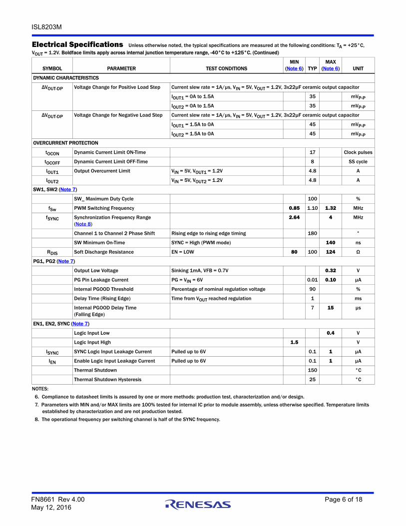
Electrical Specifications Unless otherwise noted, the typical specifications are measured at the following conditions: TA = +25°C, VOUT = 1.2V. Boldface limits apply across internal junction temperature range, -40°C to +125°C.
SYMBOL PARAMETER TEST CONDITIONSMIN
(Note 6) TYPMAX
(Note 6) UNIT
INPUT SUPPLY
VUVLO VIN Undervoltage Lockout Threshold (Note 7)
Rising 2.50 2.85 V
Hysteresis 35 130 mV
IVIN Input Supply Current (Note 7) VIN = 6V, EN1 = EN2 = 0, no load 42 µA
OUTPUT REGULATION
IOUT(DC) Output Continuous Current Range VIN = 5V, VOUT1 = 1.2V 0 3 A
VIN = 5V, VOUT2 = 1.2V 0 3 A
VIN = 5V, VOUT1 = 1.2V, in parallel mode 0 6 A
ΔVOUT1/VOUT1ΔVOUT2/VOUT2
Line Regulation VIN = 2.85V to 6V, VOUT1 = 1.2V, no load 0.25 %
VIN = 2.85V to 6V, VOUT2 = 1.2V, no load 0.25 %
VIN = 2.85V to 6V, VOUT1 = 1.2V, IOUT1 = 3A 0.25 %
VIN = 2.85V to 6V, VOUT2 = 1.2V, IOUT2 = 3A 0.25 %
ΔVOUT1/VOUT1ΔVOUT2/VOUT2
Load Regulation VIN = 5V, 2x22µF ceramic output capacitor
IOUT1 = 0A to 3A, VOUT1 = 1.2V 1 %
IOUT2 = 0A to 3A, VOUT2 = 1.2V 1 %
Output Voltage Accuracy Over line/load/temperature range -1.5 1.5 %
Over line/load/temperature/life range -2.0 2.0 %
ΔVOUT Output Ripple Voltage VIN = 5V, 3x22µF ceramic output capacitor
IOUT1 = 0A, VOUT1 = 1.2V 10 mVP-P
IOUT2 = 0A, VOUT2 = 1.2V 10 mVP-P
IOUT1 = 3A, VOUT1 = 1.2V 12 mVP-P
IOUT2 = 3A, VOUT2 = 1.2V 12 mVP-P
VFB FB1, FB2 Regulation Voltage (Note 7) 0.8 V
IFB FB1, FB2 Bias Current (Note 7) VFB = 0.75V 0.1 µA
Soft-Start Ramp Time Cycle (Note 7) SS = VDD 1.5 ms
ISS Soft-Start Charging Current (Note 7) 4 5 6 µA
FN8661 Rev 4.00 Page 5 of 18May 12, 2016
ISL8203M
DYNAMIC CHARACTERISTICS
ΔVOUT-DP Voltage Change for Positive Load Step Current slew rate = 1A/µs, VIN = 5V, VOUT = 1.2V, 3x22µF ceramic output capacitor
IOUT1 = 0A to 1.5A 35 mVP-P
IOUT2 = 0A to 1.5A 35 mVP-P
ΔVOUT-DP Voltage Change for Negative Load Step Current slew rate = 1A/µs, VIN = 5V, VOUT = 1.2V, 3x22µF ceramic output capacitor
IOUT1 = 1.5A to 0A 45 mVP-P
IOUT2 = 1.5A to 0A 45 mVP-P
OVERCURRENT PROTECTION
tOCON Dynamic Current Limit ON-Time 17 Clock pulses
tOCOFF Dynamic Current Limit OFF-Time 8 SS cycle
IOUT1 Output Overcurrent Limit VIN = 5V, VOUT1 = 1.2V 4.8 A
IOUT2 VIN = 5V, VOUT2 = 1.2V 4.8 A
SW1, SW2 (Note 7)
SW_ Maximum Duty Cycle 100 %
fSw PWM Switching Frequency 0.85 1.10 1.32 MHz
fSYNC Synchronization Frequency Range (Note 8)
2.64 4 MHz
Channel 1 to Channel 2 Phase Shift Rising edge to rising edge timing 180 °
SW Minimum On-Time SYNC = High (PWM mode) 140 ns
RDIS Soft Discharge Resistance EN = LOW 80 100 124 Ω
PG1, PG2 (Note 7)
Output Low Voltage Sinking 1mA, VFB = 0.7V 0.32 V
PG Pin Leakage Current PG = VIN = 6V 0.01 0.10 µA
Internal PGOOD Threshold Percentage of nominal regulation voltage 90 %
Delay Time (Rising Edge) Time from VOUT reached regulation 1 ms
Internal PGOOD Delay Time (Falling Edge)
7 15 µs
EN1, EN2, SYNC (Note 7)
Logic Input Low 0.4 V
Logic Input High 1.5 V
ISYNC SYNC Logic Input Leakage Current Pulled up to 6V 0.1 1 µA
IEN Enable Logic Input Leakage Current Pulled up to 6V 0.1 1 µA
Thermal Shutdown 150 °C
Thermal Shutdown Hysteresis 25 °C
NOTES:
6. Compliance to datasheet limits is assured by one or more methods: production test, characterization and/or design.
7. Parameters with MIN and/or MAX limits are 100% tested for internal IC prior to module assembly, unless otherwise specified. Temperature limits established by characterization and are not production tested.
8. The operational frequency per switching channel is half of the SYNC frequency.
Electrical Specifications Unless otherwise noted, the typical specifications are measured at the following conditions: TA = +25°C, VOUT = 1.2V. Boldface limits apply across internal junction temperature range, -40°C to +125°C. (Continued)
SYMBOL PARAMETER TEST CONDITIONSMIN
(Note 6) TYPMAX
(Note 6) UNIT
FN8661 Rev 4.00 Page 6 of 18May 12, 2016
ISL8203M
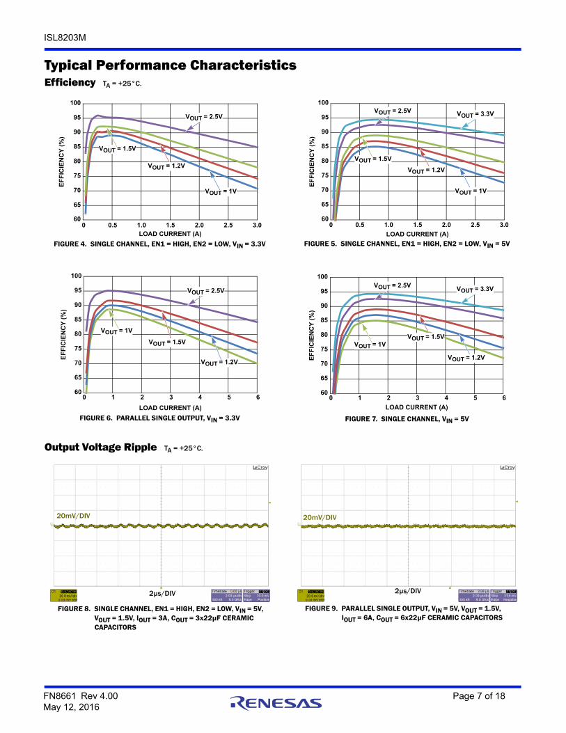
Typical Performance CharacteristicsEfficiency TA = +25°C.
FIGURE 4. SINGLE CHANNEL, EN1 = HIGH, EN2 = LOW, VIN = 3.3V FIGURE 5. SINGLE CHANNEL, EN1 = HIGH, EN2 = LOW, VIN = 5V
FIGURE 6. PARALLEL SINGLE OUTPUT, VIN = 3.3V FIGURE 7. SINGLE CHANNEL, VIN = 5V
Output Voltage Ripple TA = +25°C.
FIGURE 8. SINGLE CHANNEL, EN1 = HIGH, EN2 = LOW, VIN = 5V, VOUT = 1.5V, IOUT = 3A, COUT = 3x22µF CERAMIC CAPACITORS
FIGURE 9. PARALLEL SINGLE OUTPUT, VIN = 5V, VOUT = 1.5V, IOUT = 6A, COUT = 6x22µF CERAMIC CAPACITORS
60
65
70
75
80
85
90
95
100
0 0.5 1.0 1.5 2.0 2.5 3.0LOAD CURRENT (A)
VOUT = 1V
VOUT = 1.5V
EF
FIC
IEN
CY
(%
)
VOUT = 1.2V
VOUT = 2.5V
60
65
70
75
80
85
90
95
100
0 0.5 1.0 1.5 2.0 2.5 3.0
VOUT = 1V
VOUT = 1.5V
VOUT = 1.2V
VOUT = 2.5V VOUT = 3.3V
LOAD CURRENT (A)
EF
FIC
IEN
CY
(%
)
60
65
70
75
80
85
90
95
100
0 1 2 3 4 5 6
LOAD CURRENT (A)
VOUT = 1.2V
VOUT = 1V
EF
FIC
IEN
CY
(%
)
VOUT = 1.5V
VOUT = 2.5V
60
65
70
75
80
85
90
95
100
0 1 2 3 4 5 6
VOUT = 1.2V
VOUT = 1VVOUT = 1.5V
VOUT = 2.5V VOUT = 3.3V
LOAD CURRENT (A)
EF
FIC
IEN
CY
(%
)
20mV/DIV
2µs/DIV
20mV/DIV
2µs/DIV
FN8661 Rev 4.00 Page 7 of 18May 12, 2016
ISL8203M
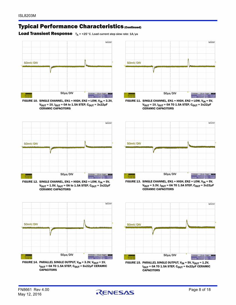
Load Transient Response TA = +25°C. Load current step slew rate: 1A/µs
FIGURE 10. SINGLE CHANNEL, EN1 = HIGH, EN2 = LOW, VIN = 3.3V, VOUT = 1V, IOUT = 0A to 1.5A STEP, COUT = 3x22µF CERAMIC CAPACITORS
FIGURE 11. SINGLE CHANNEL, EN1 = HIGH, EN2 = LOW, VIN = 5V, VOUT = 1V, IOUT = 0A TO 1.5A STEP, COUT = 3x22µF CERAMIC CAPACITORS
FIGURE 12. SINGLE CHANNEL, EN1 = HIGH, EN2 = LOW, VIN = 5V, VOUT = 1.5V, IOUT = 0A to 1.5A STEP, COUT = 3x22µF CERAMIC CAPACITORS
FIGURE 13. SINGLE CHANNEL, EN1 = HIGH, EN2 = LOW, VIN = 5V, VOUT = 3.3V, IOUT = 0A TO 1.5A STEP, COUT = 3x22µF CERAMIC CAPACITORS
FIGURE 14. PARALLEL SINGLE OUTPUT, VIN = 3.3V, VOUT = 1V, IOUT = 0A TO 1.5A STEP, COUT = 6x22µF CERAMIC CAPACITORS
FIGURE 15. PARALLEL SINGLE OUTPUT, VIN = 5V, VOUT = 1.2V, IOUT = 0A TO 1.5A STEP, COUT = 6x22µF CERAMIC CAPACITORS
Typical Performance Characteristics (Continued)
50mV/DIV
50µs/DIV
50mV/DIV
50µs/DIV
50mV/DIV
50µs/DIV
50mV/DIV
50µs/DIV
50mV/DIV
50µs/DIV
50mV/DIV
50µs/DIV
FN8661 Rev 4.00 Page 8 of 18May 12, 2016
ISL8203M
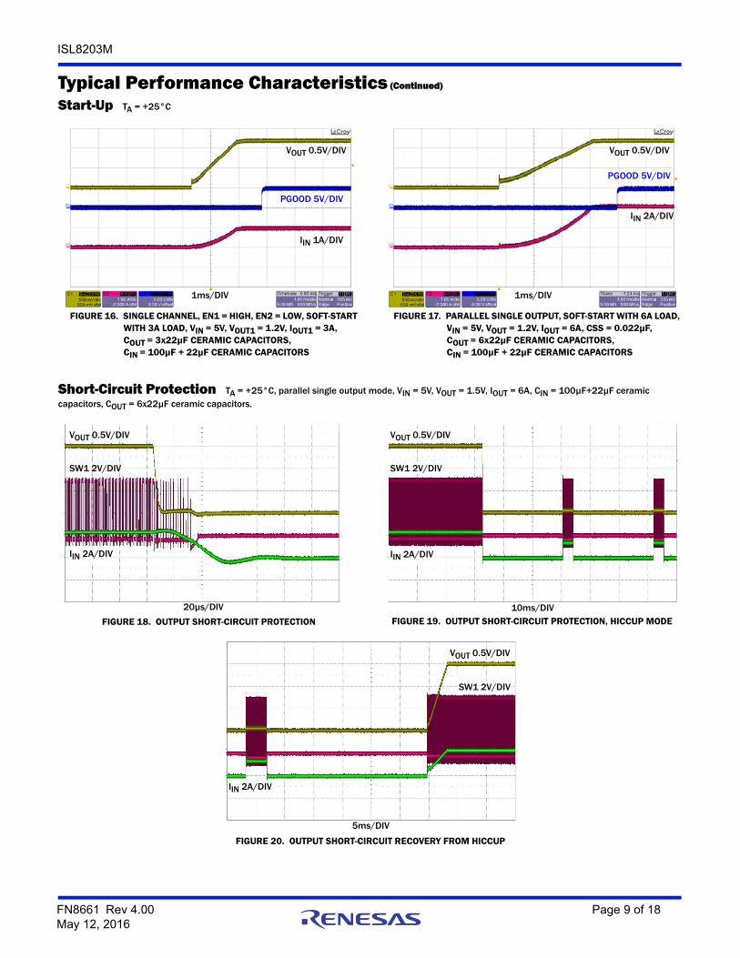
Start-Up TA = +25°C
FIGURE 16. SINGLE CHANNEL, EN1 = HIGH, EN2 = LOW, SOFT-START WITH 3A LOAD, VIN = 5V, VOUT1 = 1.2V, IOUT1 = 3A, COUT = 3x22µF CERAMIC CAPACITORS, CIN = 100µF + 22µF CERAMIC CAPACITORS
FIGURE 17. PARALLEL SINGLE OUTPUT, SOFT-START WITH 6A LOAD, VIN = 5V, VOUT = 1.2V, IOUT = 6A, CSS = 0.022µF, COUT = 6x22µF CERAMIC CAPACITORS, CIN = 100µF + 22µF CERAMIC CAPACITORS
Short-Circuit Protection TA = +25°C, parallel single output mode, VIN = 5V, VOUT = 1.5V, IOUT = 6A, CIN = 100µF+22µF ceramic capacitors, COUT = 6x22µF ceramic capacitors.
FIGURE 18. OUTPUT SHORT-CIRCUIT PROTECTION FIGURE 19. OUTPUT SHORT-CIRCUIT PROTECTION, HICCUP MODE
FIGURE 20. OUTPUT SHORT-CIRCUIT RECOVERY FROM HICCUP
Typical Performance Characteristics (Continued)
1ms/DIV
PGOOD 5V/DIV
IIN 1A/DIV
VOUT 0.5V/DIV VOUT 0.5V/DIV
1ms/DIV
PGOOD 5V/DIV
IIN 2A/DIV
VOUT 0.5V/DIV
20µs/DIV
IIN 2A/DIV
SW1 2V/DIV
VOUT 0.5V/DIV
10ms/DIV
IIN 2A/DIV
SW1 2V/DIV
5ms/DIV
IIN 2A/DIV
SW1 2V/DIV
VOUT 0.5V/DIV
FN8661 Rev 4.00 Page 9 of 18May 12, 2016
ISL8203M
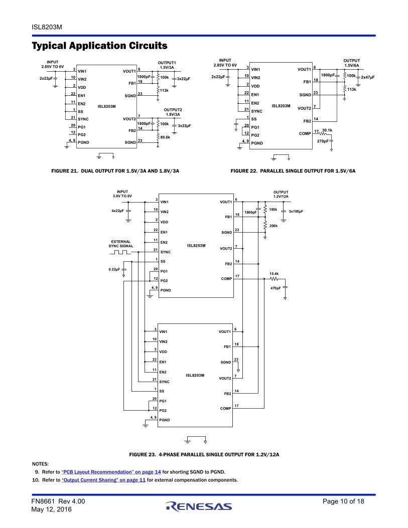
Typical Application Circuits
FIGURE 21. DUAL OUTPUT FOR 1.5V/3A AND 1.8V/3A FIGURE 22. PARALLEL SINGLE OUTPUT FOR 1.5V/6A
FIGURE 23. 4-PHASE PARALLEL SINGLE OUTPUT FOR 1.2V/12A
NOTES:
9. Refer to “PCB Layout Recommendation” on page 14 for shorting SGND to PGND.
10. Refer to “Output Current Sharing” on page 11 for external compensation components.
ISL8203M
VOUT1
FB1
SGND
VOUT2
FB2
SGND
VIN2
VDD
EN1
PG1
SYNC
EN2
PG2
PGND
OUTPUT1 1.5V/3A
VIN1100k 3x22µF
113k
80.6k
SS
100k 3x22µF
1800pF
1800pF
OUTPUT2 1.8V/3A
INPUT2.85V TO 6V 3
10
2
22
11
1
21
20
12
4, 9 23
14
7
23
18
6
2x22µF
ISL8203M
VOUT1
FB1
SGND
VOUT2
FB2
VIN2
VDD
EN1
PG1
SS
EN2
PG2
PGND
OUTPUT 1.5V/6A
VIN1100k 2x47µF
113k
SYNC
1800pF
30.1k
INPUT2.85V TO 6V
COMP
270pF
3
10
2
22
11
21
1
20
12
4, 9
6
18
23
7
14
17
2x22µF
ISL8203M
VOUT1
FB1
SGND
VOUT2
FB2
VIN2
VDD
EN1
PG1
SS
EN2
PG2
PGND
OUTPUT 1.2V/12A
VIN1
100k 3x100µF
200k
SYNC
1800pF
15.4k
INPUT2.8V TO 6V
COMP
470pF
ISL8203M
VOUT1
FB1
SGND
VOUT2
FB2
VIN2
VDD
EN1
PG1
SS
EN2
PG2
PGND
VIN1
SYNC
COMP
3
10
2
22
11
21
1
20
12
4, 9
6
18
23
7
14
17
3
10
2
22
11
21
1
20
12
4, 9
6
18
23
7
14
17
EXTERNAL SYNC SIGNAL
4x22µF
0.22µF
FN8661 Rev 4.00 Page 10 of 18May 12, 2016
ISL8203M
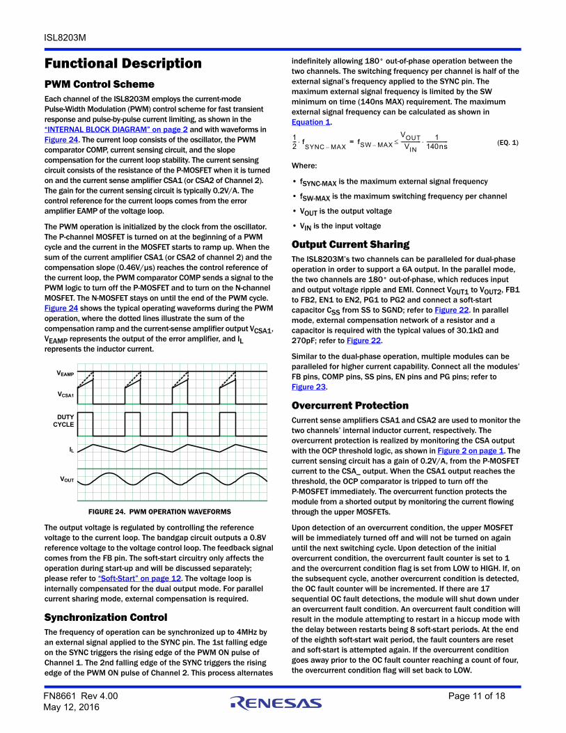
Functional DescriptionPWM Control SchemeEach channel of the ISL8203M employs the current-mode Pulse-Width Modulation (PWM) control scheme for fast transient response and pulse-by-pulse current limiting, as shown in the “INTERNAL BLOCK DIAGRAM” on page 2 and with waveforms in Figure 24. The current loop consists of the oscillator, the PWM comparator COMP, current sensing circuit, and the slope compensation for the current loop stability. The current sensing circuit consists of the resistance of the P-MOSFET when it is turned on and the current sense amplifier CSA1 (or CSA2 of Channel 2). The gain for the current sensing circuit is typically 0.2V/A. The control reference for the current loops comes from the error amplifier EAMP of the voltage loop.
The PWM operation is initialized by the clock from the oscillator. The P-channel MOSFET is turned on at the beginning of a PWM cycle and the current in the MOSFET starts to ramp up. When the sum of the current amplifier CSA1 (or CSA2 of channel 2) and the compensation slope (0.46V/µs) reaches the control reference of the current loop, the PWM comparator COMP sends a signal to the PWM logic to turn off the P-MOSFET and to turn on the N-channel MOSFET. The N-MOSFET stays on until the end of the PWM cycle. Figure 24 shows the typical operating waveforms during the PWM operation, where the dotted lines illustrate the sum of the compensation ramp and the current-sense amplifier output VCSA1, VEAMP represents the output of the error amplifier, and IL represents the inductor current.
The output voltage is regulated by controlling the reference voltage to the current loop. The bandgap circuit outputs a 0.8V reference voltage to the voltage control loop. The feedback signal comes from the FB pin. The soft-start circuitry only affects the operation during start-up and will be discussed separately; please refer to “Soft-Start” on page 12. The voltage loop is internally compensated for the dual output mode. For parallel current sharing mode, external compensation is required.
Synchronization ControlThe frequency of operation can be synchronized up to 4MHz by an external signal applied to the SYNC pin. The 1st falling edge on the SYNC triggers the rising edge of the PWM ON pulse of Channel 1. The 2nd falling edge of the SYNC triggers the rising edge of the PWM ON pulse of Channel 2. This process alternates
indefinitely allowing 180° out-of-phase operation between the two channels. The switching frequency per channel is half of the external signal’s frequency applied to the SYNC pin. The maximum external signal frequency is limited by the SW minimum on time (140ns MAX) requirement. The maximum external signal frequency can be calculated as shown in Equation 1.
Where:
• fSYNC-MAX is the maximum external signal frequency
• fSW-MAX is the maximum switching frequency per channel
• VOUT is the output voltage
• VIN is the input voltage
Output Current SharingThe ISL8203M’s two channels can be paralleled for dual-phase operation in order to support a 6A output. In the parallel mode, the two channels are 180° out-of-phase, which reduces input and output voltage ripple and EMI. Connect VOUT1 to VOUT2, FB1 to FB2, EN1 to EN2, PG1 to PG2 and connect a soft-start capacitor CSS from SS to SGND; refer to Figure 22. In parallel mode, external compensation network of a resistor and a capacitor is required with the typical values of 30.1kΩ and 270pF; refer to Figure 22.
Similar to the dual-phase operation, multiple modules can be paralleled for higher current capability. Connect all the modules’ FB pins, COMP pins, SS pins, EN pins and PG pins; refer to Figure 23.
Overcurrent ProtectionCurrent sense amplifiers CSA1 and CSA2 are used to monitor the two channels’ internal inductor current, respectively. The overcurrent protection is realized by monitoring the CSA output with the OCP threshold logic, as shown in Figure 2 on page 1. The current sensing circuit has a gain of 0.2V/A, from the P-MOSFET current to the CSA_ output. When the CSA1 output reaches the threshold, the OCP comparator is tripped to turn off the P-MOSFET immediately. The overcurrent function protects the module from a shorted output by monitoring the current flowing through the upper MOSFETs.
Upon detection of an overcurrent condition, the upper MOSFET will be immediately turned off and will not be turned on again until the next switching cycle. Upon detection of the initial overcurrent condition, the overcurrent fault counter is set to 1 and the overcurrent condition flag is set from LOW to HIGH. If, on the subsequent cycle, another overcurrent condition is detected, the OC fault counter will be incremented. If there are 17 sequential OC fault detections, the module will shut down under an overcurrent fault condition. An overcurrent fault condition will result in the module attempting to restart in a hiccup mode with the delay between restarts being 8 soft-start periods. At the end of the eighth soft-start wait period, the fault counters are reset and soft-start is attempted again. If the overcurrent condition goes away prior to the OC fault counter reaching a count of four, the overcurrent condition flag will set back to LOW.
FIGURE 24. PWM OPERATION WAVEFORMS
VEAMP
VCSA1
DUTY CYCLE
IL
VOUT
12--- f
SYNC MAX–fSW MAX–
VOUTVIN---------------- 1
140ns-----------------= (EQ. 1)
FN8661 Rev 4.00 Page 11 of 18May 12, 2016
ISL8203M
If the negative current of the internal inductor reaches -2.5A, the module enters negative overcurrent protection. At this point, all switching stops and the module enters tri-state mode while the pull-down MOSFET discharges the output until it reaches normal regulation voltage, then the module restarts.
Power-Good There are two independent power-good signals for each of the two outputs via the FB pins. PG1 monitors the output Channel 1 and PG2 monitors the output Channel 2. When powering up, the open-collector power-on reset output holds low for about 1ms after VOUT reaches within ±8% of the preset voltage. The PG pins do not require a pull-up resistor.
UVLO (Undervoltage Lockout)When the input voltage is below the Undervoltage Lockout (UVLO) threshold, the module is disabled. The maximum UVLO threshold is 2.85V.
EnableThe enable (EN) input allows the user to control the turning on or off of the module for purposes such as power-up sequencing. Each channel of the ISL8203M can be turned on or off independently through the EN pins. Once the module is enabled, there is typically a 600µs delay for waking up the bandgap reference, then the soft start-up begins.
Soft-StartThe ISL8203M employs an internal digital soft-start circuitry which minimizes input inrush current during the start-up. The soft-start circuitry outputs a ramp reference to both the voltage loop and the current loop. The two ramps limit the inductor current rising speed as well as the output voltage rising speed so that the output voltage rises in a controlled fashion. At the beginning of the soft-start internal, when the voltage on the FB pin is less than 0.5V, the PWM oscillator frequency is forced to half of the normal frequency. During the soft-start, the module cannot sink current, behaving as in diode emulated mode for the soft-start time.
If SS pin is tied to VIN, the soft-start time is an internally fixed 1.5ms. For parallel current sharing mode operation, connect a capacitor CSS from SS to SGND. CSS should not be larger than 33nF. This capacitor along with the internal current source of 5µA sets the soft-start time tSS, which can be calculated as shown in Equation 2.
Discharge ModeWhen a transition to shutdown mode occurs, or the output undervoltage fault latch is set, the module’s output discharges to PGND through an internal 100Ω switch.
Power MOSFETsThe internal power MOSFETs are optimize for best efficiency. The ON-resistance for the P-MOSFET is typically 50mΩ and the ON-resistance for the N-MOSFET is typically 50mΩ.
100% Duty Cycle OperationThe ISL8203M offers 100% duty cycle operation. When the input voltage drops to a level that the ISL8203M can no longer maintain the regulation at the output, the module completely turns on the P-MOSFET. The maximum dropout voltage under the 100% duty-cycle operation is the product of the load current and the ON-resistance of the P-MOSFET.
Thermal ShutdownThe ISL8203M offers built-in over-temperature protection. When the junction temperature reaches +150°C, the module is completely shut down. As the temperature drops to +125°C, the ISL8203M resumes operation by stepping through a soft-start.
Applications InformationProgramming the Output VoltageThe output voltage of the module is programmed by an external resistor divider between VOUT, FB and SGND pins, as shown in Figure 21. The output voltage can be calculated as shown in Equation 3.
Where:
• RFBTOP is the top feedback resistor
• RFBBOT is the bottom feedback resistor
The top resistor is typically a 100kΩ value, and a 1800pF capacitor is recommended to be connected in parallel if the output capacitors are all ceramic capacitors or bulk capacitors with low ESR (equivalent series resistance). The value of the bottom resistor for different output voltages is shown in Table 1.
Please note that the output voltage accuracy is also dependent on the resistor accuracy of RFBTOP and RFBBOT. The user needs to select high accuracy resistors (i.e., 0.5%) in order to achieve the overall output accuracy.
Input Capacitor SelectionLow Equivalent Series Resistance (ESR) ceramic capacitance is recommended to reduce input voltage ripple and decouple between the VIN and PGND of each channel. This capacitance
tSS ms 0.16 CSS nF = (EQ. 2)
TABLE 1. VALUE OF BOTTOM RESISTOR FOR DIFFERENT OUTPUT VOLTAGES (VOUT vs RFBBOT)
RFBTOP (kΩ) VOUT (V) RFBBOT (kΩ)
100 0.8 open
100 1.0 402
100 1.2 200
100 1.5 113
100 1.8 80.6
100 2.5 47.5
100 3.3 32.4
VOUT 0.8V 1RFBTOPRFBBOT-----------------------+
= (EQ. 3)
FN8661 Rev 4.00 Page 12 of 18May 12, 2016
ISL8203M
reduces voltage ringing created by the switching current across parasitic circuit elements. The ceramic capacitors should be placed as closely as possible to the module pins. A minimum of 22µF ceramic capacitance for each channel is recommended.
A bulk input capacitance may also be needed if the input source does not have enough output capacitance. A typical value of bulk input capacitor is 100µF. In such conditions, this bulk input capacitance can supply the current during output load transient conditions.
Output Capacitor SelectionCeramic capacitors are typically used as the output capacitors for the ISL8203M. A minimum output capacitance of 2x22µF per phase is recommended. Bulk output capacitors that have adequately low Equivalent Series Resistance (ESR), such as low ESR polymer capacitors or a low ESR tantalum capacitor, may also be used in combination with the ceramic capacitors, depending on the output voltage ripple and transient requirements.
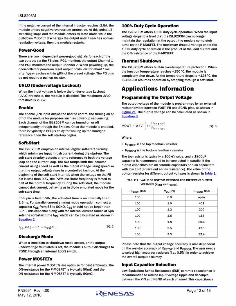
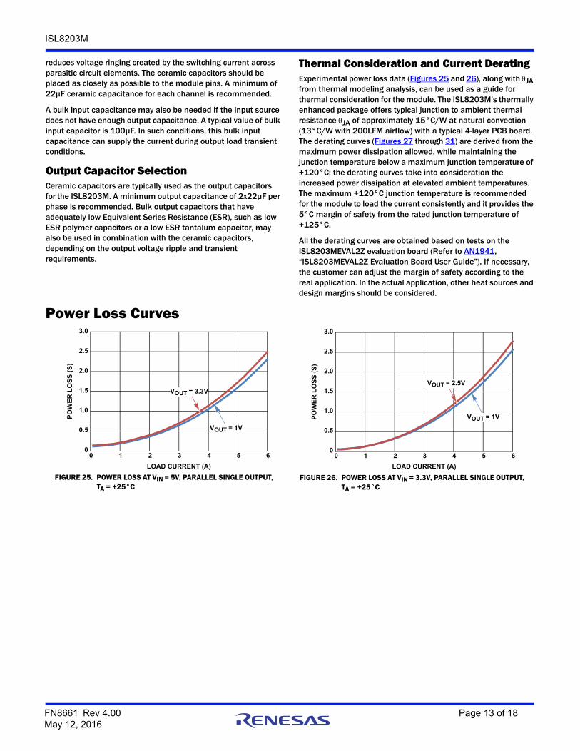
Thermal Consideration and Current DeratingExperimental power loss data (Figures 25 and 26), along with JA from thermal modeling analysis, can be used as a guide for thermal consideration for the module. The ISL8203M’s thermally enhanced package offers typical junction to ambient thermal resistance JA of approximately 15°C/W at natural convection (13°C/W with 200LFM airflow) with a typical 4-layer PCB board. The derating curves (Figures 27 through 31) are derived from the maximum power dissipation allowed, while maintaining the junction temperature below a maximum junction temperature of +120°C; the derating curves take into consideration the increased power dissipation at elevated ambient temperatures. The maximum +120°C junction temperature is recommended for the module to load the current consistently and it provides the 5°C margin of safety from the rated junction temperature of +125°C.
All the derating curves are obtained based on tests on the ISL8203MEVAL2Z evaluation board (Refer to AN1941, “ISL8203MEVAL2Z Evaluation Board User Guide”). If necessary, the customer can adjust the margin of safety according to the real application. In the actual application, other heat sources and design margins should be considered.
Power Loss Curves
FIGURE 25. POWER LOSS AT VIN = 5V, PARALLEL SINGLE OUTPUT, TA = +25°C
FIGURE 26. POWER LOSS AT VIN = 3.3V, PARALLEL SINGLE OUTPUT, TA = +25°C
0
0.5
1.0
1.5
2.0
2.5
3.0
0 1 2 3 4 5 6
LOAD CURRENT (A)
PO
WE
R L
OS
S (
S)
VOUT = 1V
VOUT = 3.3V
0
0.5
1.0
1.5
2.0
2.5
3.0
0 1 2 3 4 5 6
VOUT = 1V
VOUT = 2.5V
LOAD CURRENT (A)
PO
WE
R L
OS
S (
S)
FN8661 Rev 4.00 Page 13 of 18May 12, 2016
ISL8203M
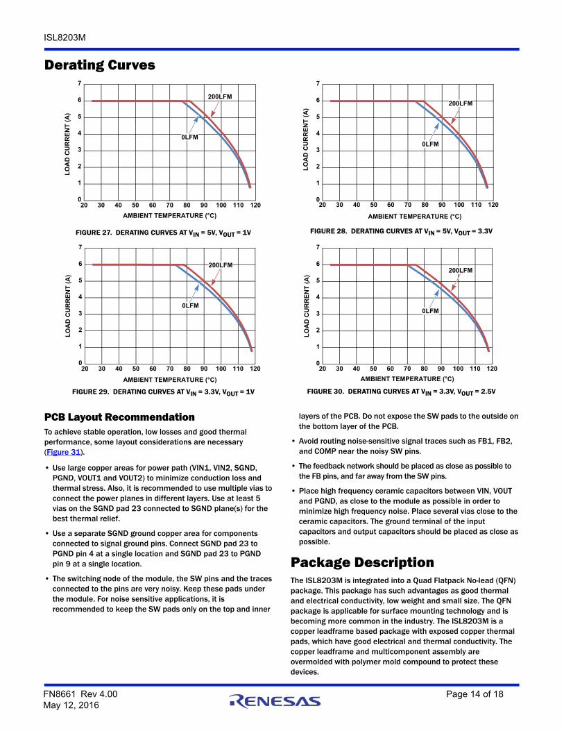
PCB Layout RecommendationTo achieve stable operation, low losses and good thermal performance, some layout considerations are necessary (Figure 31).
• Use large copper areas for power path (VIN1, VIN2, SGND, PGND, VOUT1 and VOUT2) to minimize conduction loss and thermal stress. Also, it is recommended to use multiple vias to connect the power planes in different layers. Use at least 5 vias on the SGND pad 23 connected to SGND plane(s) for the best thermal relief.
• Use a separate SGND ground copper area for components connected to signal ground pins. Connect SGND pad 23 to PGND pin 4 at a single location and SGND pad 23 to PGND pin 9 at a single location.
• The switching node of the module, the SW pins and the traces connected to the pins are very noisy. Keep these pads under the module. For noise sensitive applications, it is recommended to keep the SW pads only on the top and inner
layers of the PCB. Do not expose the SW pads to the outside on the bottom layer of the PCB.
• Avoid routing noise-sensitive signal traces such as FB1, FB2, and COMP near the noisy SW pins.
• The feedback network should be placed as close as possible to the FB pins, and far away from the SW pins.
• Place high frequency ceramic capacitors between VIN, VOUT and PGND, as close to the module as possible in order to minimize high frequency noise. Place several vias close to the ceramic capacitors. The ground terminal of the input capacitors and output capacitors should be placed as close as possible.
Package Description The ISL8203M is integrated into a Quad Flatpack No-lead (QFN) package. This package has such advantages as good thermal and electrical conductivity, low weight and small size. The QFN package is applicable for surface mounting technology and is becoming more common in the industry. The ISL8203M is a copper leadframe based package with exposed copper thermal pads, which have good electrical and thermal conductivity. The copper leadframe and multicomponent assembly are overmolded with polymer mold compound to protect these devices.
Derating Curves
FIGURE 27. DERATING CURVES AT VIN = 5V, VOUT = 1V FIGURE 28. DERATING CURVES AT VIN = 5V, VOUT = 3.3V
FIGURE 29. DERATING CURVES AT VIN = 3.3V, VOUT = 1V FIGURE 30. DERATING CURVES AT VIN = 3.3V, VOUT = 2.5V
0
1
2
3
4
5
6
7
20 30 40 50 60 70 80 90 100 110 120
AMBIENT TEMPERATURE (°C)
LO
AD
CU
RR
EN
T (
A)
0LFM
200LFM
0
1
2
3
4
5
6
7
20 30 40 50 60 70 80 90 100 110 120
AMBIENT TEMPERATURE (°C)
LO
AD
CU
RR
EN
T (
A)
0LFM
200LFM
0
1
2
3
4
5
6
7
20 30 40 50 60 70 80 90 100 110 120
AMBIENT TEMPERATURE (°C)
LO
AD
CU
RR
EN
T (
A)
0LFM
200LFM
0
1
2
3
4
5
6
7
20 30 40 50 60 70 80 90 100 110 120
AMBIENT TEMPERATURE (°C)
LO
AD
CU
RR
EN
T (
A)
0LFM
200LFM
FN8661 Rev 4.00 Page 14 of 18May 12, 2016
ISL8203M
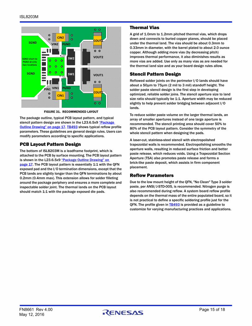
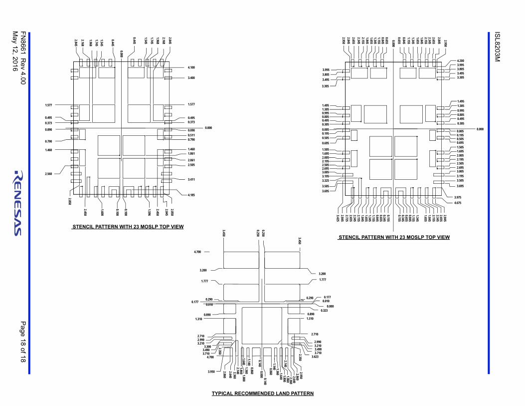
The package outline, typical PCB layout pattern, and typical stencil pattern design are shown in the L23.6.5x9 “Package Outline Drawing” on page 17. TB493 shows typical reflow profile parameters. These guidelines are general design rules. Users can modify parameters according to specific applications.
PCB Layout Pattern DesignThe bottom of ISL8203M is a leadframe footprint, which is attached to the PCB by surface mounting. The PCB layout pattern is shown in the L23.6.5x9 “Package Outline Drawing” on page 17. The PCB layout pattern is essentially 1:1 with the QFN exposed pad and the I/O termination dimensions, except that the PCB lands are slightly longer than the QFN terminations by about 0.2mm (0.4mm max). This extension allows for solder filleting around the package periphery and ensures a more complete and inspectable solder joint. The thermal lands on the PCB layout should match 1:1 with the package exposed die pads.
Thermal ViasA grid of 1.0mm to 1.2mm pitched thermal vias, which drops down and connects to buried copper planes, should be placed under the thermal land. The vias should be about 0.3mm to 0.33mm in diameter, with the barrel plated to about 2.0 ounce copper. Although adding more vias (by decreasing pitch) improves thermal performance, it also diminishes results as more vias are added. Use only as many vias as are needed for the thermal land size and as your board design rules allow.
Stencil Pattern DesignReflowed solder joints on the perimeter I/O lands should have about a 50µm to 75µm (2 mil to 3 mil) standoff height. The solder paste stencil design is the first step in developing optimized, reliable solder joins. The stencil aperture size to land size ratio should typically be 1:1. Aperture width may be reduced slightly to help prevent solder bridging between adjacent I/O lands.
To reduce solder paste volume on the larger thermal lands, an array of smaller apertures instead of one large aperture is recommended. The stencil printing area should cover 50% to 80% of the PCB layout pattern. Consider the symmetry of the whole stencil pattern when designing the pads.
A laser-cut, stainless-steel stencil with electropolished trapezoidal walls is recommended. Electropolishing smooths the aperture walls, resulting in reduced surface friction and better paste release, which reduces voids. Using a Trapezoidal Section Aperture (TSA) also promotes paste release and forms a brick-like paste deposit, which assists in firm component placement.
Reflow ParametersDue to the low mount height of the QFN, "No Clean" Type 3 solder paste, per ANSI/J-STD-005, is recommended. Nitrogen purge is also recommended during reflow. A system board reflow profile depends on the thermal mass of the entire populated board, so it is not practical to define a specific soldering profile just for the QFN. The profile given in TB493 is provided as a guideline to customize for varying manufacturing practices and applications.
FIGURE 31. RECOMMENDED LAYOUT
FN8661 Rev 4.00 Page 15 of 18May 12, 2016
ISL8203M
Intersil products are manufactured, assembled and tested utilizing ISO9001 quality systems as notedin the quality certifications found at www.intersil.com/en/support/qualandreliability.html
Intersil products are sold by description only. Intersil may modify the circuit design and/or specifications of products at any time without notice, provided that such modification does not, in Intersil's sole judgment, affect the form, fit or function of the product. Accordingly, the reader is cautioned to verify that datasheets are current before placing orders. Information furnished by Intersil is believed to be accurate and reliable. However, no responsibility is assumed by Intersil or its subsidiaries for its use; nor for any infringements of patents or other rights of third parties which may result from its use. No license is granted by implication or otherwise under any patent or patent rights of Intersil or its subsidiaries.
For information regarding Intersil Corporation and its products, see www.intersil.com
For additional products, see www.intersil.com/en/products.html
© Copyright Intersil Americas LLC 2014-2016. All Rights Reserved.All trademarks and registered trademarks are the property of their respective owners.
About IntersilIntersil Corporation is a leading provider of innovative power management and precision analog solutions. The company's products address some of the largest markets within the industrial and infrastructure, mobile computing and high-end consumer markets.
For the most updated datasheet, application notes, related documentation and related parts, please see the respective product information page found at www.intersil.com.
You may report errors or suggestions for improving this datasheet by visiting www.intersil.com/ask.
Reliability reports are also available from our website at www.intersil.com/support.
Revision History The revision history provided is for informational purposes only and is believed to be accurate, but not warranted. Please go to the web to make sure that you have the latest revision.
DATE REVISION CHANGE
May 12, 2016 FN8661.4 Updated Note 1 in the Ordering Information table.Updated POD to the latest revision changes are as follows:
-Updated bottom view by adding two dimensions and moved two dimension labels over so they are easier to read.
January 19, 2015 FN8661.3 Updated “Package Outline Drawing” on page 17 with latest revision. Corrected/updated recommended PCB land pattern and added recommended stencil patterns.
August 28, 2014 FN8661.2 Added to sentence that is under “Programming the Output Voltage” on page 12 after “...in parallel.”, which reads “if the output capacitors are all ceramic capacitors or bulk capacitors with low ESR (equivalent series resistance)."Replaced Schematics on page 1 and page 10.Figure 2, added the XYZ dimension on the picture (9.0mmx6.5mmx1.83mm.Figure 23, changed the "113k" resistor to "200k".
July 23, 2014 FN8661.1 Added Evaluation Board to “Ordering Information” on page 4.
June 23, 2014 FN8661.0 Initial Release
FN8661 Rev 4.00 Page 16 of 18May 12, 2016
ISL8203M
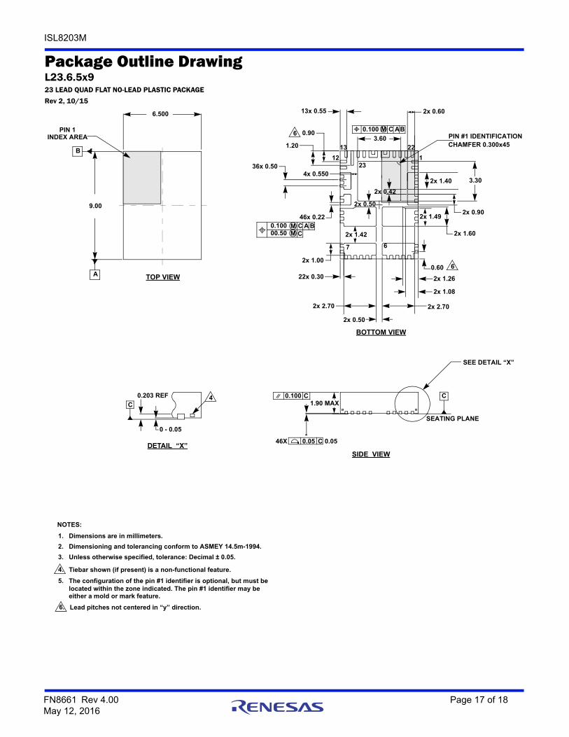
FN8661 Rev 4.00 Page 17 of 18May 12, 2016
Package Outline DrawingL23.6.5x923 LEAD QUAD FLAT NO-LEAD PLASTIC PACKAGE
Rev 2, 10/15
BOTTOM VIEW
TOP VIEW
located within the zone indicated. The pin #1 identifier may be
Tiebar shown (if present) is a non-functional feature.
The configuration of the pin #1 identifier is optional, but must be5.
either a mold or mark feature.
4.
Dimensions are in millimeters.1.
NOTES:
6.500
PIN 1INDEX AREA
B
A
9.00
13x 0.55 2x 0.60
0.90
1.20
36x 0.504x 0.550
46x 0.22
22x 0.30
2x 2.70
2x 0.50
2x 2.70
0.60
2x 1.60
2x 0.90
3.302x 1.40
2x 1.42
2x 1.49
2x 1.00
2x 0.50
2x 0.42
3.60 PIN #1 IDENTIFICATIONCHAMFER 0.300x45
67
2312
13 22
1
0.10000.50
MM
C A B
0.100 M C A
C
B
SEE DETAIL “X”
C
SEATING PLANE
1.90 MAX0.100 C
0.05 C46X 0.05
SIDE VIEWDETAIL “X”
C
0.203 REF
0 - 0.05
4
Dimensioning and tolerancing conform to ASMEY 14.5m-1994.2.
Unless otherwise specified, tolerance: Decimal ± 0.05. 3.
6
6
Lead pitches not centered in “y” direction.6.
2x 1.08
2x 1.26
FN
866
1R
ev 4
.00
Pa
ge 1
8 of 18
May 12
, 201
6
ISL8
203
M
0.090
STENCIL PATTERN WITH 23 MOSLP TOP VIEW
2.845
2.168
1.968
1.7451.545
0.445
0.445
1.545
1.7451.968
2.168
2.8452.8502.845
2.450
1.596
2.850
1.577
0.4950.373
1.460
0.790
2.560
0.495
4.100
3.400
1.577
0.373
0.511
0.0000.090
0.790
1.4601.861
2.0612.505
3.411
4.185
3.305
2.950
3.495
1.845
2.8452.6552.3452.155
1.155
1.6551.345
2.950
0.8450.655
0.6550.8451.1551.3451.6551.8452.1552.3452.6552.845
3.9953.805
0.695
3.305
1.4951.3050.9950.8050.4950.3050.0050.1950.505
2.005
1.5051.695
2.195
3.005
2.5052.695
3.695
3.1953.3253.505
3.4252.845
2.6552.725
2.1552.345
1.155
1.8451.6551.345
0.155
0.8450.6550.345
0.1550.3450.6550.8451.1551.345
1.6551.8452.1552.3452.6552.845
4.2003.9953.8053.495
0.305
1.4951.3050.9950.8050.495
0.000
3.695
0.0050.1950.5050.6951.5051.6952.0052.1952.5052.6953.0053.1953.505
3.9754.675
STENCIL PATTERN WITH 23 MOSLP TOP VIEW
0.100
0.100
1.600
2.450
0.000
0.000
TYPICAL RECOMMENDED LAND PATTERN
4.700
2.860
0.2500.250 3.450
3.2003.200
1.777 1.777
0.1770.010
0.290
0.0000.323
0.8901.310
2.710
2.9903.2103.4903.710
3.623
0.1770.2900.010
1.3100.890
2.7102.9903.210
3.3003.490
4.7003.710
2.350
3.950 2.6402.360
2.1401.860 1.800
1.6401.140
1.360
0.1400.860 0.000 0.1400.860
1.3601.140
1.8001.640 2.640
1.8602.360
2.8602.950
2.3502.140
3.450