TA78L05F, TA78L06F, TA78L07F, TA78L08F, … term stability ΔVOUT/Δt 1 ― ― 21 ― mV/kh Ripple...
19
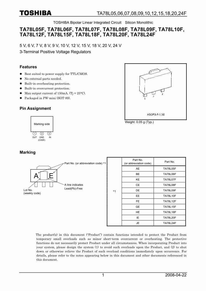
TA78L05,06,07,08,09,10,12,15,18,20,24F 2008-04-22 1 TOSHIBA Bipolar Linear Integrated Circuit Silicon Monolithic TA78L05F, TA78L06F, TA78L07F, TA78L08F, TA78L09F, TA78L10F, TA78L12F, TA78L15F, TA78L18F, TA78L20F, TA78L24F 5 V, 6 V, 7 V, 8 V, 9 V, 10 V, 12 V, 15 V, 18 V, 20 V, 24 V 3-Terminal Positive Voltage Regulators Features z Best suited to power supply for TTL/CMOS. z No external parts needed. z Built-in overheating protection. z Built-in overcurrent protection. z Max output current of 150mA. (T j = 25°C). z Packaged in PW-mini (SOT-89). Pin Assignment OUT 1 2 IN GND (CASE) Marking side 3 Marking Part No. (or abbreviation code) Part No. AE TA78L05F BE TA78L06F KE TA78L07F CE TA78L08F DE TA78L09F EE TA78L10F FE TA78L12F GE TA78L15F HE TA78L18F IE TA78L20F *1 JE TA78L24F The product(s) in this document (“Product”) contain functions intended to protect the Product from temporary small overloads such as minor short-term overcurrent or overheating. The protective functions do not necessarily protect Product under all circumstances. When incorporating Product into your system, please design the system (1) to avoid such overloads upon the Product, and (2) to shut down or otherwise relieve the Product of such overload conditions immediately upon occurrence. For details, please refer to the notes appearing below in this document and other documents referenced in this document. Weight: 0.05 g (Typ.) A E Part No. (or abbreviation code) *1 Lot No. (weekly code) A line indicates Lead(Pb)-Free
Transcript of TA78L05F, TA78L06F, TA78L07F, TA78L08F, … term stability ΔVOUT/Δt 1 ― ― 21 ― mV/kh Ripple...
TA78L05,06,07,08,09,10,12,15,18,20,24F
2008-04-22 1
TOSHIBA Bipolar Linear Integrated Circuit Silicon Monolithic
TA78L05F, TA78L06F, TA78L07F, TA78L08F, TA78L09F, TA78L10F, TA78L12F, TA78L15F, TA78L18F, TA78L20F, TA78L24F 5 V, 6 V, 7 V, 8 V, 9 V, 10 V, 12 V, 15 V, 18 V, 20 V, 24 V 3-Terminal Positive Voltage Regulators
Features Best suited to power supply for TTL/CMOS. No external parts needed. Built-in overheating protection. Built-in overcurrent protection. Max output current of 150mA. (Tj = 25°C). Packaged in PW-mini (SOT-89).
Pin Assignment
OUT
1 2
IN GND (CASE)
Marking side
3
Marking Part No.
(or abbreviation code) Part No.
AE TA78L05F
BE TA78L06F
KE TA78L07F
CE TA78L08F
DE TA78L09F
EE TA78L10F
FE TA78L12F
GE TA78L15F
HE TA78L18F
IE TA78L20F
*1
JE TA78L24F
The product(s) in this document (“Product”) contain functions intended to protect the Product from temporary small overloads such as minor short-term overcurrent or overheating. The protective functions do not necessarily protect Product under all circumstances. When incorporating Product into your system, please design the system (1) to avoid such overloads upon the Product, and (2) to shut down or otherwise relieve the Product of such overload conditions immediately upon occurrence. For details, please refer to the notes appearing below in this document and other documents referenced in this document.
Weight: 0.05 g (Typ.)
A E
Part No. (or abbreviation code) *1
Lot No. (weekly code)
A line indicates Lead(Pb)-Free
TA78L05,06,07,08,09,10,12,15,18,20,24F
2008-04-22 2
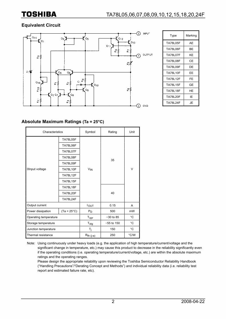
Equivalent Circuit
Type Marking
TA78L05F AE
TA78L06F BE
TA78L07F KE
TA78L08F CE
TA78L09F DE
TA78L10F EE
TA78L12F FE
TA78L15F GE
TA78L18F HE
TA78L20F IE
TA78L24F JE
Absolute Maximum Ratings (Ta = 25°C)
Characteristics Symbol Rating Unit
TA78L05F
TA78L06F
TA78L07F
TA78L08F
TA78L09F
TA78L10F
TA78L12F
TA78L15F
35
TA78L18F
TA78L20F
0Input voltage
TA78L24F
VIN
40
V
Output current IOUT 0.15 A
Power dissipation (Ta = 25°C) PD 500 mW
Operating temperature Topr −30 to 85 °C
Storage temperature Tstg −55 to 150 °C
Junction temperature Tj 150 °C
Thermal resistance Rth (j-a) 250 °C/W
Note: Using continuously under heavy loads (e.g. the application of high temperature/current/voltage and the significant change in temperature, etc.) may cause this product to decrease in the reliability significantly even if the operating conditions (i.e. operating temperature/current/voltage, etc.) are within the absolute maximum ratings and the operating ranges. Please design the appropriate reliability upon reviewing the Toshiba Semiconductor Reliability Handbook (“Handling Precautions”/“Derating Concept and Methods”) and individual reliability data (i.e. reliability test report and estimated failure rate, etc).
TA78L05,06,07,08,09,10,12,15,18,20,24F
2008-04-22 3
TA78L05F Electrical Characteristics (Unless otherwise specified, VIN = 10 V, IOUT = 40 mA, CIN = 0.33 μF, COUT = 0.1 μF, 0°C ≤ Tj ≤ 125°C)
Characteristics Symbol Test
Circuit Test Condition Min Typ. Max Unit
Output voltage VOUT 1 Tj = 25°C 4.75 5.0 5.25 V
7.0 V ≤ VIN ≤ 20 V ― 55 150Line regulation Reg·line 1 Tj = 25°C
8.0 V ≤ VIN ≤ 20 V ― 45 100mV
1.0 mA ≤ IOUT ≤ 100 mA ― 11 60 Load regulation Reg·load 1 Tj = 25°C
1.0 mA ≤ IOUT ≤ 40 mA ― 5.0 30 mV
7.0 V ≤ VIN ≤ 20 V, 1.0 mA ≤ IOUT ≤ 40 mA 4.65 ― 5.35
Output voltage VOUT 1 Tj = 25°C1.0 mA ≤ IOUT ≤ 70 mA 4.65 ― 5.35
V
Tj = 25°C ― 3.1 6.0 Quiescent current IB 1
Tj = 125°C ― ― 5.5 mA
8.0 V ≤ VIN ≤ 20 V ― ― 1.5 Quiescent current change ΔIB 1 Tj = 25°C
1.0 mA ≤ IOUT ≤ 40 mA ― ― 0.1 mA
Output noise voltage VNO 2 Ta = 25°C, 10 Hz ≤ f ≤ 100 kHz ― 40 ― μVrms
Long term stability ΔVOUT/Δt 1 ― ― 12 ― mV/kh
Ripple rejection ratio R.R. 3 f = 120 Hz, 8.0 V ≤ VIN ≤ 18 V, Tj = 25°C 41 49 ― dB
Dropout voltage VD 1 Tj = 25°C ― 1.7 ― V
Average temperature coefficient of output voltage TCVO 1 IOUT = 5 mA ― −0.6 ― mV/°C

TA78L05,06,07,08,09,10,12,15,18,20,24F
2008-04-22 4
TA78L06F Electrical Characteristics (Unless otherwise specified, VIN = 11 V, IOUT = 40 mA, CIN = 0.33 μF, COUT = 0.1 μF, 0°C ≤ Tj ≤ 125°C)
Characteristics Symbol Test
Circuit Test Condition Min Typ. Max Unit
Output voltage VOUT 1 Tj = 25°C 5.7 6.0 6.3 V
8.1 V ≤ VIN ≤ 21 V ― 50 150Line regulation Reg·line 1 Tj = 25°C
9.0 V ≤ VIN ≤ 21 V ― 45 110mV
1.0 mA ≤ IOUT ≤ 100 mA ― 12 70 Load regulation Reg·load 1 Tj = 25°C
1.0 mA ≤ IOUT ≤ 40 mA ― 5.5 35 mV
8.1 V ≤ VIN ≤ 21 V, 1.0 mA ≤ IOUT ≤ 40 mA 5.58 ― 6.42
Output voltage VOUT 1 Tj = 25°C1.0 mA ≤ IOUT ≤ 70 mA 5.58 ― 6.42
V
Tj = 25°C ― 3.1 6.0 Quiescent current IB 1
Tj = 125°C ― ― 5.5 mA
9.0 V ≤ VIN ≤ 20 V ― ― 1.5 Quiescent current change ΔIB 1 Tj = 25°C
1.0 mA ≤ IOUT ≤ 40 mA ― ― 0.1 mA
Output noise voltage VNO 2 Ta = 25°C, 10 Hz ≤ f ≤ 100 kHz ― 40 ― μVrms
Long term stability ΔVOUT/Δt 1 ― ― 14 ― mV/kh
Ripple rejection ratio R.R. 3 f = 120 Hz, 9.0 V ≤ VIN ≤ 19 V, Tj = 25°C 39 47 ― dB
Dropout voltage VD 1 Tj = 25°C ― 1.7 ― V
Average temperature coefficient of output voltage TCVO 1 IOUT = 5 mA ― −0.7 ― mV/°C

TA78L05,06,07,08,09,10,12,15,18,20,24F
2008-04-22 5
TA78L07F Electrical Characteristics (Unless otherwise specified, VIN = 12 V, IOUT = 40 mA, CIN = 0.33 μF, COUT = 0.1 μF, 0°C ≤ Tj ≤ 125°C)
Characteristics Symbol Test
Circuit Test Condition Min Typ. Max Unit
Output voltage VOUT 1 Tj = 25°C 6.65 7.0 7.35 V
9.2 V ≤ VIN ≤ 22 V ― 50 160Line regulation Reg·line 1 Tj = 25°C
10 V ≤ VIN ≤ 22 V ― 45 115mV
1.0 mA ≤ IOUT ≤ 100 mA ― 13 75 Load regulation Reg·load 1 Tj = 25°C
1.0 mA ≤ IOUT ≤ 40 mA ― 6.0 40 mV
9.2 V ≤ VIN ≤ 22 V, 1.0 mA ≤ IOUT ≤ 40 mA 6.51 ― 7.49
Output voltage VOUT 1 Tj = 25°C1.0 mA ≤ IOUT ≤ 70 mA 6.51 ― 7.49
V
Tj = 25°C ― 3.1 6.5 Quiescent current IB 1
Tj = 125°C ― ― 6.0 mA
10 V ≤ VIN ≤ 22 V ― ― 1.5 Quiescent current change ΔIB 1 Tj = 25°C
1.0 mA ≤ IOUT ≤ 40 mA ― ― 0.1 mA
Output noise voltage VNO 2 Ta = 25°C, 10 Hz ≤ f ≤ 100 kHz ― 50 ― μVrms
Long term stability ΔVOUT/Δt 1 ― ― 17 ― mV/kh
Ripple rejection ratio R.R. 3 f = 120 Hz, 10 V ≤ VIN ≤ 20 V, Tj = 25°C 37 46 ― dB
Dropout voltage VD 1 Tj = 25°C ― 1.7 ― V
Average temperature coefficient of output voltage TCVO 1 IOUT = 5 mA ― −0.75 ― mV/°C

TA78L05,06,07,08,09,10,12,15,18,20,24F
2008-04-22 6
TA78L08F Electrical Characteristics (Unless otherwise specified, VIN = 14 V, IOUT = 40 mA, CIN = 0.33 μF, COUT = 0.1 μF, 0°C ≤ Tj ≤ 125°C)
Characteristics Symbol Test
Circuit Test Condition Min Typ. Max Unit
Output voltage VOUT 1 Tj = 25°C 7.6 8.0 8.4 V
10.5 V ≤ VIN ≤ 23 V ― 20 175Line regulation Reg·line 1 Tj = 25°C
11 V ≤ VIN ≤ 23 V ― 12 125mV
1.0 mA ≤ IOUT ≤ 100 mA ― 15 80 Load regulation Reg·load 1 Tj = 25°C
1.0 mA ≤ IOUT ≤ 40 mA ― 7.0 40 mV
10.5 V ≤ VIN ≤ 23 V, 1.0 mA ≤ IOUT ≤ 40 mA 7.44 ― 8.56
Output voltage VOUT 1 Tj = 25°C1.0 mA ≤ IOUT ≤ 70 mA 7.44 ― 8.56
V
Tj = 25°C ― 3.1 6.5 Quiescent current IB 1
Tj = 125°C ― ― 6.0 mA
11 V ≤ VIN ≤ 23 V ― ― 1.5 Quiescent current change ΔIB 1 Tj = 25°C
1.0 mA ≤ IOUT ≤ 40 mA ― ― 0.1 mA
Output noise voltage VNO 2 Ta = 25°C, 10 Hz ≤ f ≤ 100 kHz ― 60 ― μVrms
Long term stability ΔVOUT/Δt 1 ― ― 20 ― mV/kh
Ripple rejection ratio R.R. 3 f = 120 Hz, 12 V ≤ VIN ≤ 23 V, Tj = 25°C 37 45 ― dB
Dropout voltage VD 1 Tj = 25°C ― 1.7 ― V
Average temperature coefficient of output voltage TCVO 1 IOUT = 5 mA ― −0.8 ― mV/°C

TA78L05,06,07,08,09,10,12,15,18,20,24F
2008-04-22 7
TA78L09F Electrical Characteristics (Unless otherwise specified, VIN = 15 V, IOUT = 40 mA, CIN = 0.33 μF, COUT = 0.1 μF, 0°C ≤ Tj ≤ 125°C)
Characteristics Symbol Test
Circuit Test Condition Min Typ. Max Unit
Output voltage VOUT 1 Tj = 25°C 8.55 9.0 9.45 V
11.4 V ≤ VIN ≤ 24 V ― 80 200Line regulation Reg·line 1 Tj = 25°C
12 V ≤ VIN ≤ 24 V ― 20 160mV
1.0 mA ≤ IOUT ≤ 100 mA ― 17 90 Load regulation Reg·load 1 Tj = 25°C
1.0 mA ≤ IOUT ≤ 40 mA ― 8.0 45 mV
11.4 V ≤ VIN ≤ 24 V, 1.0 mA ≤ IOUT ≤ 40 mA 8.37 ― 9.63
Output voltage VOUT 1 Tj = 25°C1.0 mA ≤ IOUT ≤ 70 mA 8.37 ― 9.63
V
Tj = 25°C ― 3.2 6.5 Quiescent current IB 1
Tj = 125°C ― ― 6.0 mA
12 V ≤ VIN ≤ 24 V ― ― 1.5 Quiescent current change ΔIB 1 Tj = 25°C
1.0 mA ≤ IOUT ≤ 40 mA ― ― 0.1 mA
Output noise voltage VNO 2 Ta = 25°C, 10 Hz ≤ f ≤ 100 kHz ― 65 ― μVrms
Long term stability ΔVOUT/Δt 1 ― ― 21 ― mV/kh
Ripple rejection ratio R.R. 3 f = 120 Hz, 12 V ≤ VIN ≤ 24 V, Tj = 25°C 36 44 ― dB
Dropout voltage VD 1 Tj = 25°C ― 1.7 ― V
Average temperature coefficient of output voltage TCVO 1 IOUT = 5 mA ― −0.85 ― mV/°C

TA78L05,06,07,08,09,10,12,15,18,20,24F
2008-04-22 8
TA78L10F Electrical Characteristics (Unless otherwise specified, VIN = 16 V, IOUT = 40 mA, CIN = 0.33 μF, COUT = 0.1 μF, 0°C ≤ Tj ≤ 125°C)
Characteristics Symbol Test
Circuit Test Condition Min Typ. Max Unit
Output voltage VOUT 1 Tj = 25°C 9.5 10 10.5 V
12.5 V ≤ VIN ≤ 25 V ― 80 230Line regulation Reg·line 1 Tj = 25°C
13 V ≤ VIN ≤ 25 V ― 30 170mV
1.0 mA ≤ IOUT ≤ 100 mA ― 18 90 Load regulation Reg·load 1 Tj = 25°C
1.0 mA ≤ IOUT ≤ 40 mA ― 8.5 45 mV
12.5 V ≤ VIN ≤ 25 V, 1.0 mA ≤ IOUT ≤ 40 mA 9.3 ― 10.7
Output voltage VOUT 1 Tj = 25°C1.0 mA ≤ IOUT ≤ 70 mA 9.3 ― 10.7
V
Tj = 25°C ― 3.2 6.5 Quiescent current IB 1
Tj = 125°C ― ― 6.0 mA
13 V ≤ VIN ≤ 25 V ― ― 1.5 Quiescent current change ΔIB 1 Tj = 25°C
1.0 mA ≤ IOUT ≤ 40 mA ― ― 0.1 mA
Output noise voltage VNO 2 Ta = 25°C, 10 Hz ≤ f ≤ 100 kHz ― 70 ― μVrms
Long term stability ΔVOUT/Δt 1 ― ― 22 ― mV/kh
Ripple rejection ratio R.R. 3 f = 120 Hz, 13 V ≤ VIN ≤ 24 V, Tj = 25°C 36 43 ― dB
Dropout voltage VD 1 Tj = 25°C ― 1.7 ― V
Average temperature coefficient of output voltage TCVO 1 IOUT = 5 mA ― −0.9 ― mV/°C

TA78L05,06,07,08,09,10,12,15,18,20,24F
2008-04-22 9
TA78L12F Electrical Characteristics (Unless otherwise specified, VIN = 19 V, IOUT = 40 mA, CIN = 0.33 μF, COUT = 0.1 μF, 0°C ≤ Tj ≤ 125°C)
Characteristics Symbol Test
Circuit Test Condition Min Typ. Max Unit
Output voltage VOUT 1 Tj = 25°C 11.4 12 12.6 V
14.5 V ≤ VIN ≤ 27 V ― 120 250Line regulation Reg·line 1 Tj = 25°C
16 V ≤ VIN ≤ 27 V ― 100 200mV
1.0 mA ≤ IOUT ≤ 100 mA ― 20 100Load regulation Reg·load 1 Tj = 25°C
1.0 mA ≤ IOUT ≤ 40 mA ― 10 50 mV
14.5 V ≤ VIN ≤ 27 V, 1.0 mA ≤ IOUT ≤ 40 mA 11.16 ― 12.84
Output voltage VOUT 1 Tj = 25°C1.0 mA ≤ IOUT ≤ 70 mA 11.16 ― 12.84
V
Tj = 25°C ― 3.2 6.5 Quiescent current IB 1
Tj = 125°C ― ― 6.0 mA
16 V ≤ VIN ≤ 27 V ― ― 1.5 Quiescent current change ΔIB 1 Tj = 25°C
1.0 mA ≤ IOUT ≤ 40 mA ― ― 0.1 mA
Output noise voltage VNO 2 Ta = 25°C, 10 Hz ≤ f ≤ 100 kHz ― 80 ― μVrms
Long term stability ΔVOUT/Δt 1 ― ― 24 ― mV/kh
Ripple rejection ratio R.R. 3 f = 120 Hz, 15 V ≤ VIN ≤ 25 V, Tj = 25°C 36 41 ― dB
Dropout voltage VD 1 Tj = 25°C ― 1.7 ― V
Average temperature coefficient of output voltage TCVO 1 IOUT = 5 mA ― −1.0 ― mV/°C

TA78L05,06,07,08,09,10,12,15,18,20,24F
2008-04-22 10
TA78L15F Electrical Characteristics (Unless otherwise specified, VIN = 23 V, IOUT = 40 mA, CIN = 0.33 μF, COUT = 0.1 μF, 0°C ≤ Tj ≤ 125°C)
Characteristics Symbol Test
Circuit Test Condition Min Typ. Max Unit
Output voltage VOUT 1 Tj = 25°C 14.25 15 15.75 V
17.5 V ≤ VIN ≤ 30 V ― 130 300Line regulation Reg·line 1 Tj = 25°C
20 V ≤ VIN ≤ 30 V ― 110 250mV
1.0 mA ≤ IOUT ≤ 100 mA ― 25 150Load regulation Reg·load 1 Tj = 25°C
1.0 mA ≤ IOUT ≤ 40 mA ― 12 75 mV
17.5 V ≤ VIN ≤ 30 V, 1.0 mA ≤ IOUT ≤ 40 mA 13.95 ― 16.05
Output voltage VOUT 1 Tj = 25°C1.0 mA ≤ IOUT ≤ 70 mA 13.95 ― 16.05
V
Tj = 25°C ― 3.3 6.5 Quiescent current IB 1
Tj = 125°C ― ― 6.0 mA
20 V ≤ VIN ≤ 30 V ― ― 1.5 Quiescent current change ΔIB 1 Tj = 25°C
1.0 mA ≤ IOUT ≤ 40 mA ― ― 0.1 mA
Output noise voltage VNO 2 Ta = 25°C, 10 Hz ≤ f ≤ 100 kHz ― 90 ― μVrms
Long term stability ΔVOUT/Δt 1 ― ― 30 ― mV/kh
Ripple rejection ratio R.R. 3 f = 120 Hz, 18.5 V ≤ VIN ≤ 28.5 V, Tj = 25°C 34 40 ― dB
Dropout voltage VD 1 Tj = 25°C ― 1.7 ― V
Average temperature coefficient of output voltage TCVO 1 IOUT = 5 mA ― −1.3 ― mV/°C

TA78L05,06,07,08,09,10,12,15,18,20,24F
2008-04-22 11
TA78L18F Electrical Characteristics (Unless otherwise specified, VIN = 27 V, IOUT = 40 mA, CIN = 0.33 μF, COUT = 0.1 μF, 0°C ≤ Tj ≤ 125°C)
Characteristics Symbol Test
Circuit Test Condition Min Typ. Max Unit
Output voltage VOUT 1 Tj = 25°C 17.1 18 18.9 V
21.4 V ≤ VIN ≤ 33 V ― 32 325Line regulation Reg·line 1 Tj = 25°C
22 V ≤ VIN ≤ 33 V ― 27 275mV
1.0 mA ≤ IOUT ≤ 100 mA ― 30 170Load regulation Reg·load 1 Tj = 25°C
1.0 mA ≤ IOUT ≤ 40 mA ― 15 75 mV
21.4 V ≤ VIN ≤ 33 V, 1.0 mA ≤ IOUT ≤ 40 mA 16.74 ― 19.26
Output voltage VOUT 1 Tj = 25°C1.0 mA ≤ IOUT ≤ 70 mA 16.74 ― 19.26
V
Tj = 25°C ― 3.3 6.5 Quiescent current IB 1
Tj = 125°C ― ― 6.0 mA
22 V ≤ VIN ≤ 33 V ― ― 1.5 Quiescent current change ΔIB 1 Tj = 25°C
1.0 mA ≤ IOUT ≤ 40 mA ― ― 0.1 mA
Output noise voltage VNO 2 Ta = 25°C, 10 Hz ≤ f ≤ 100 kHz ― 150 ― μVrms
Long term stability ΔVOUT/Δt 1 ― ― 45 ― mV/kh
Ripple rejection ratio R.R. 3 f = 120 Hz, 23 V ≤ VIN ≤ 33 V, Tj = 25°C 32 38 ― dB
Dropout voltage VD 1 Tj = 25°C ― 1.7 ― V
Average temperature coefficient of output voltage TCVO 1 IOUT = 5 mA ― −1.5 ― mV/°C
TA78L05,06,07,08,09,10,12,15,18,20,24F
2008-04-22 12
TA78L20F Electrical Characteristics (Unless otherwise specified, VIN = 29 V, IOUT = 40 mA, CIN = 0.33 μF, COUT = 0.1 μF, 0°C ≤ Tj ≤ 125°C)
Characteristics Symbol Test
Circuit Test Condition Min Typ. Max Unit
Output voltage VOUT 1 Tj = 25°C 19.0 20 21.0 V
23.5 V ≤ VIN ≤ 35 V ― 33 330Line regulation Reg·line 1 Tj = 25°C
24 V ≤ VIN ≤ 35 V ― 28 285mV
1.0 mA ≤ IOUT ≤ 100 mA ― 33 180Load regulation Reg·load 1 Tj = 25°C
1.0 mA ≤ IOUT ≤ 40 mA ― 17 90 mV
23.5 V ≤ VIN ≤ 35 V, 1.0 mA ≤ IOUT ≤ 40 mA 18.6 ― 21.4
Output voltage VOUT 1 Tj = 25°C1.0 mA ≤ IOUT ≤ 70 mA 18.6 ― 21.4
V
Tj = 25°C ― 3.3 6.5 Quiescent current IB 1
Tj = 125°C ― ― 6.0 mA
24 V ≤ VIN ≤ 35 V ― ― 1.5 Quiescent current change ΔIB 1 Tj = 25°C
1.0 mA ≤ IOUT ≤ 40 mA ― ― 0.1 mA
Output noise voltage VNO 2 Ta = 25°C, 10 Hz ≤ f ≤ 100 kHz ― 170 ― μVrms
Long term stability ΔVOUT/Δt 1 ― ― 49 ― mV/kh
Ripple rejection ratio R.R. 3 f = 120 Hz, 25 V ≤ VIN ≤ 35 V, Tj = 25°C 31 37 ― dB
Dropout voltage VD 1 Tj = 25°C ― 1.7 ― V
Average temperature coefficient of output voltage TCVO 1 IOUT = 5 mA ― −1.7 ― mV/°C

TA78L05,06,07,08,09,10,12,15,18,20,24F
2008-04-22 13
TA78L24F Electrical Characteristics (Unless otherwise specified, VIN = 33 V, IOUT = 40 mA, CIN = 0.33 μF, COUT = 0.1 μF, 0°C ≤ Tj ≤ 125°C)
Characteristics Symbol Test
Circuit Test Condition Min Typ. Max Unit
Output voltage VOUT 1 Tj = 25°C 22.8 24 25.2 V
27.5 V ≤ VIN ≤ 38 V ― 35 350Line regulation Reg·line 1 Tj = 25°C
28 V ≤ VIN ≤ 38 V ― 30 300mV
1.0 mA ≤ IOUT ≤ 100 mA ― 40 200Load regulation Reg·load 1 Tj = 25°C
1.0 mA ≤ IOUT ≤ 40 mA ― 20 100mV
27.5 V ≤ VIN ≤ 38 V, 1.0 mA ≤ IOUT ≤ 40 mA 22.32 ― 25.68
Output voltage VOUT 1 Tj = 25°C1.0 mA ≤ IOUT ≤ 70 mA 22.32 ― 25.68
V
Tj = 25°C ― 3.5 6.5 Quiescent current IB 1
Tj = 125°C ― ― 6.0 mA
28 V ≤ VIN ≤ 38 V ― ― 1.5 Quiescent current change ΔIB 1 Tj = 25°C
1.0 mA ≤ IOUT ≤ 40 mA ― ― 0.1 mA
Output noise voltage VNO 2 Ta = 25°C, 10 Hz ≤ f ≤ 100 kHz ― 200 ― μVrms
Long term stability ΔVOUT/Δt 1 ― ― 56 ― mV/kh
Ripple rejection ratio R.R. 3 f = 120 Hz, 29 V ≤ VIN ≤ 39 V, Tj = 25°C 31 35 ― dB
Dropout voltage VD 1 Tj = 25°C ― 1.7 ― V
Average temperature coefficient of output voltage TCVO 1 IOUT = 5 mA ― −2.0 ― mV/°C
TA78L05,06,07,08,09,10,12,15,18,20,24F
2008-04-22 14
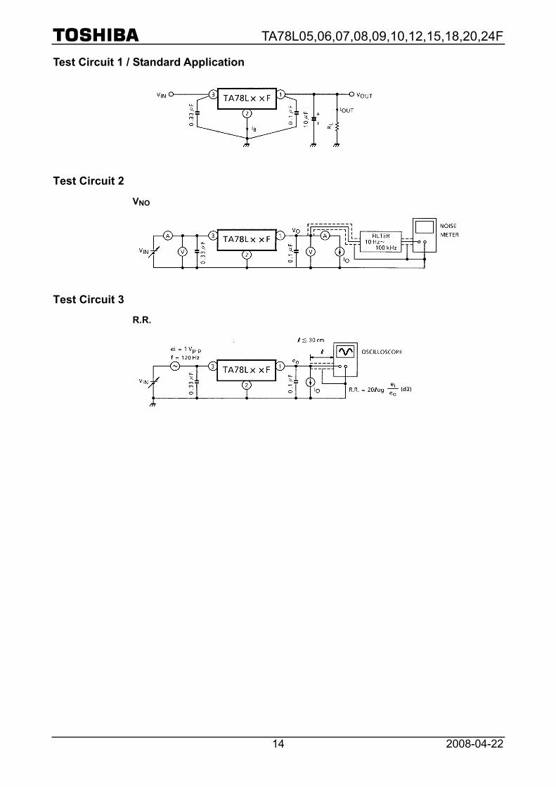
Test Circuit 1 / Standard Application
Test Circuit 2
VNO
Test Circuit 3
R.R.

TA78L05,06,07,08,09,10,12,15,18,20,24F
2008-04-22 15
TA78L05,06,07,08,09,10,12,15,18,20,24F
2008-04-22 16
TA78L05,06,07,08,09,10,12,15,18,20,24F
2008-04-22 17
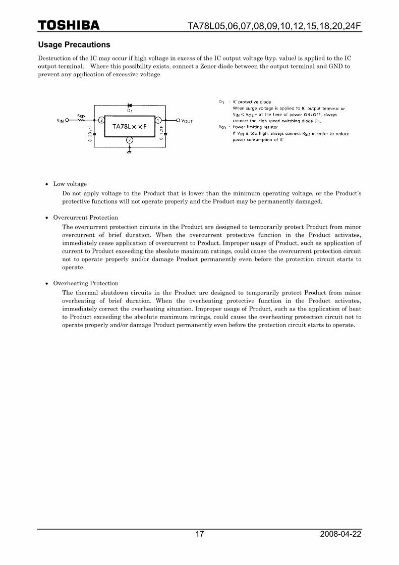
Usage Precautions Destruction of the IC may occur if high voltage in excess of the IC output voltage (typ. value) is applied to the IC output terminal. Where this possibility exists, connect a Zener diode between the output terminal and GND to prevent any application of excessive voltage.
• Low voltage Do not apply voltage to the Product that is lower than the minimum operating voltage, or the Product’s protective functions will not operate properly and the Product may be permanently damaged.
• Overcurrent Protection
The overcurrent protection circuits in the Product are designed to temporarily protect Product from minor overcurrent of brief duration. When the overcurrent protective function in the Product activates, immediately cease application of overcurrent to Product. Improper usage of Product, such as application of current to Product exceeding the absolute maximum ratings, could cause the overcurrent protection circuit not to operate properly and/or damage Product permanently even before the protection circuit starts to operate.
• Overheating Protection
The thermal shutdown circuits in the Product are designed to temporarily protect Product from minor overheating of brief duration. When the overheating protective function in the Product activates, immediately correct the overheating situation. Improper usage of Product, such as the application of heat to Product exceeding the absolute maximum ratings, could cause the overheating protection circuit not to operate properly and/or damage Product permanently even before the protection circuit starts to operate.
TA78L05,06,07,08,09,10,12,15,18,20,24F
2008-04-22 18
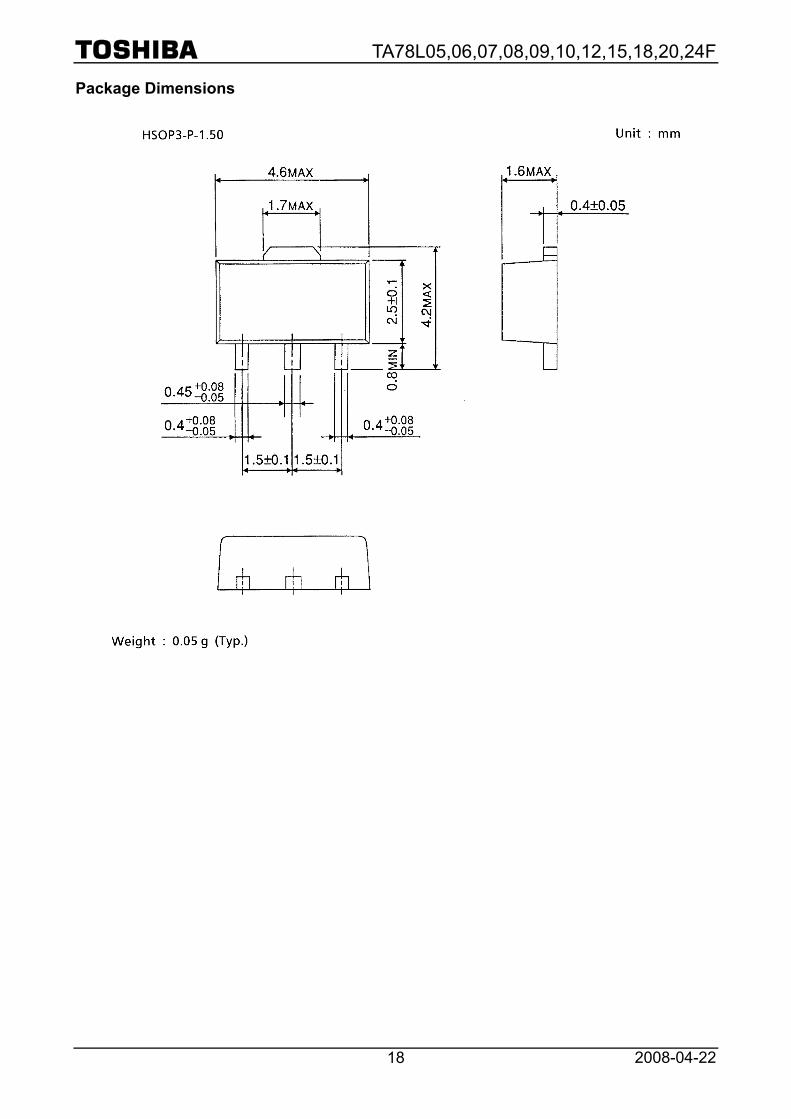
Package Dimensions
TA78L05,06,07,08,09,10,12,15,18,20,24F
2008-04-22 19
RESTRICTIONS ON PRODUCT USE 20070701-EN GENERAL
• The information contained herein is subject to change without notice.
• TOSHIBA is continually working to improve the quality and reliability of its products. Nevertheless, semiconductor devices in general can malfunction or fail due to their inherent electrical sensitivity and vulnerability to physical stress. It is the responsibility of the buyer, when utilizing TOSHIBA products, to comply with the standards of safety in making a safe design for the entire system, and to avoid situations in which a malfunction or failure of such TOSHIBA products could cause loss of human life, bodily injury or damage to property. In developing your designs, please ensure that TOSHIBA products are used within specified operating ranges as set forth in the most recent TOSHIBA products specifications. Also, please keep in mind the precautions and conditions set forth in the “Handling Guide for Semiconductor Devices,” or “TOSHIBA Semiconductor Reliability Handbook” etc.
• The TOSHIBA products listed in this document are intended for usage in general electronics applications (computer, personal equipment, office equipment, measuring equipment, industrial robotics, domestic appliances, etc.).These TOSHIBA products are neither intended nor warranted for usage in equipment that requires extraordinarily high quality and/or reliability or a malfunction or failure of which may cause loss of human life or bodily injury (“Unintended Usage”). Unintended Usage include atomic energy control instruments, airplane or spaceship instruments, transportation instruments, traffic signal instruments, combustion control instruments, medical instruments, all types of safety devices, etc.. Unintended Usage of TOSHIBA products listed in his document shall be made at the customer’s own risk.
• The products described in this document shall not be used or embedded to any downstream products of which manufacture, use and/or sale are prohibited under any applicable laws and regulations.
• The information contained herein is presented only as a guide for the applications of our products. No responsibility is assumed by TOSHIBA for any infringements of patents or other rights of the third parties which may result from its use. No license is granted by implication or otherwise under any patents or other rights of TOSHIBA or the third parties.
• Please contact your sales representative for product-by-product details in this document regarding RoHS compatibility. Please use these products in this document in compliance with all applicable laws and regulations that regulate the inclusion or use of controlled substances. Toshiba assumes no liability for damage or losses occurring as a result of noncompliance with applicable laws and regulations.
![««[1 έl Lå∂rðл Ðεl яåýø / R.R.]»»](https://static.fdocument.org/doc/165x107/568caaf61a28ab186da3a46f/1-l-lard-dl-ayo-rr.jpg)
![««[2 Σl мάr ∂ε Løš мøпšτruõš / R.R.]»»](https://static.fdocument.org/doc/165x107/568caadd1a28ab186da33ecb/2-l-r-los-osruos-rr.jpg)
![Game of Thrones.Το τραγούδι της Φωτιάς και του Πάγου -George R.R. Martin [SuperNova Team]](https://static.fdocument.org/doc/165x107/55cf9985550346d0339dc8e7/game-of-thrones-.jpg)


![««[Løš Σжþë∂iεn‡έš Ðël Šέмi∂ïøš / R.R.]»»](https://static.fdocument.org/doc/165x107/568caad51a28ab186da31e07/los-beins-del-siios-rr.jpg)


![««[3 Þэrçצ Jαçkšðп γ ιa мαι∂îçïøп ∂eι τiтαп / R.R.]»»](https://static.fdocument.org/doc/165x107/568caaed1a28ab186da37c6b/3-brc-jcksd-a-icio-e-i-.jpg)