An Extended-Range Ethernet and Clock Distribution Circuit for Distributed Sensor Networks
For price, delivery and to place orders: Hittite Microwave Corporation, 2 Elizabeth Drive, Chelmsford, MA 01824Phone: 978-250-3343 Fax: 978-250-3373 Order On-line at www.hittite.com
Application Support: Phone: 978-250-3343 or [email protected]
Dat
a C
on
ve
rt
er
s -
sM
t
1
HMCAD5831LP9BEv02.0713
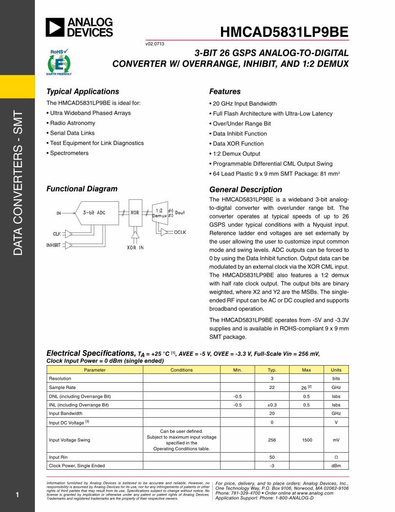
3-BIT 26 GSPS ANALOG-TO-DIGITALCONVERTER W/ OVERRANGE, INHIBIT, AND 1:2 DEMUX
the HMCaD5831LP9Be is a wideband 3-bit analog-to-digital converter with over/under range bit. the converter operates at typical speeds of up to 26 GsPs under typical conditions with a nyquist input. reference ladder end voltages are set externally by the user allowing the user to customize input common mode and swing levels. aDC outputs can be forced to 0 by using the Data Inhibit function. output data can be modulated by an external clock via the Xor CML input. the HMCaD5831LP9Be also features a 1:2 demux with half rate clock output. the output bits are binary weighted, where X2 and Y2 are the MsBs. the single-ended rF input can be aC or DC coupled and supports broadband operation.
the HMCaD5831LP9Be operates from -5v and -3.3v supplies and is available in roHs-compliant 9 x 9 mm sMt package.
General Description
Features
Functional Diagram
Typical Applicationsthe HMCaD5831LP9Be is ideal for:
• Ultra Wideband Phased arrays
• radio astronomy
• serial Data Links
• test equipment for Link Diagnostics
• spectrometers
Electrical Specifications, TA = +25 °C [1], AVEE = -5 V, OVEE = -3.3 V, Full-Scale Vin = 256 mV, Clock Input Power = 0 dBm (single ended)
Parameter Conditions Min. typ. Max Units
resolution 3 bits
sample rate 22 26 [2] GHz
DnL (including overrange Bit) -0.5 0.5 lsbs
InL (including overrange Bit) -0.5 ±0.3 0.5 lsbs
Input Bandwidth 20 GHz
Input DC voltage [3] 0 v
Input voltage swing
Can be user defined.subject to maximum input voltage
specified in the operating Conditions table.
256 1500 mv
Input rin 50 Ω
Clock Power, single ended -3 dBm
• 20 GHz Input Bandwidth
• Full Flash architecture with Ultra-Low Latency
• over/Under range Bit
• Data Inhibit Function
• Data Xor Function
• 1:2 Demux output
• Programmable Differential CML output swing
• 64 Lead Plastic 9 x 9 mm sMt Package: 81 mm2
Information furnished by Analog Devices is believed to be accurate and reliable. However, no responsibility is assumed by Analog Devices for its use, nor for any infringements of patents or other rights of third parties that may result from its use. Specifications subject to change without notice. No license is granted by implication or otherwise under any patent or patent rights of Analog Devices. Trademarks and registered trademarks are the property of their respective owners.
For price, delivery, and to place orders: Analog Devices, Inc., One Technology Way, P.O. Box 9106, Norwood, MA 02062-9106 Phone: 781-329-4700 • Order online at www.analog.com Application Support: Phone: 1-800-ANALOG-D
For price, delivery and to place orders: Hittite Microwave Corporation, 2 Elizabeth Drive, Chelmsford, MA 01824Phone: 978-250-3343 Fax: 978-250-3373 Order On-line at www.hittite.com
Application Support: Phone: 978-250-3343 or [email protected]
Dat
a C
on
ve
rt
er
s -
sM
t
2
HMCAD5831LP9BEv02.0713
3-BIT 26 GSPS ANALOG-TO-DIGITALCONVERTER W/ OVERRANGE, INHIBIT, AND 1:2 DEMUX
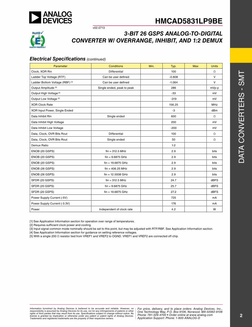
Electrical Specifications (continued)
Parameter Conditions Min. typ. Max Units
Clock, Xor rin Differential 100 Ω
Ladder top voltage (rtF) Can be user defined -0.808 v
Ladder Bottom voltage (rBF) [4] Can be user defined -1.064 v
output amplitude [5] single ended, peak to peak 286 mvp-p
output High voltage [5] -33 mv
output Low voltage [5] -319 mv
Xor Clock rate 156.25 MHz
Xor Input Power, single ended -3 dBm
Data Inhibit rin single ended 600 Ω
Data Inhibit High voltage 200 mv
Data Inhibit Low voltage -200 mv
Data, Clock, ovr Bits rout Differential 100 Ω
Data, Clock, ovr Bits rout single ended 50 Ω
Demux ratio 1:2
enoB (20 GsPs) fin = 312.5 MHz 2.9 bits
enoB (20 GsPs) fin = 9.6875 GHz 2.9 bits
enoB (20 GsPs) fin = 19.6875 GHz 2.9 bits
enoB (26 GsPs) fin = 406.25 MHz 2.9 bits
enoB (26 GsPs) fin = 12.5938 GHz 2.9 bits
sFDr (20 GsPs) fin = 312.5 MHz 24.7 dBFs
sFDr (20 GsPs) fin = 9.6875 GHz 25.7 dBFs
sFDr (20 GsPs) fin = 19.6875 GHz 27.2 dBFs
Power supply Current (-5v) 725 ma
Power supply Current (-3.3v) 176 ma
Power Independent of clock rate 4.2 W
[1] see application Information section for operation over range of temperatures.[2] requires sufficient clock power and cooling.[3] Input signal common mode nominally should be set to this point, but may be adjusted with rtF/rBF. see application Information section.[4] see application Information section for guidance on setting reference voltages.[5] With a single 200 Ω resistor tied from vreF1 and vreF2 to oGnD. vreF1 and vreF2 are connected off chip.
Information furnished by Analog Devices is believed to be accurate and reliable. However, no responsibility is assumed by Analog Devices for its use, nor for any infringements of patents or other rights of third parties that may result from its use. Specifications subject to change without notice. No license is granted by implication or otherwise under any patent or patent rights of Analog Devices. Trademarks and registered trademarks are the property of their respective owners.
For price, delivery, and to place orders: Analog Devices, Inc., One Technology Way, P.O. Box 9106, Norwood, MA 02062-9106 Phone: 781-329-4700 • Order online at www.analog.com Application Support: Phone: 1-800-ANALOG-D
For price, delivery and to place orders: Hittite Microwave Corporation, 2 Elizabeth Drive, Chelmsford, MA 01824Phone: 978-250-3343 Fax: 978-250-3373 Order On-line at www.hittite.com
Application Support: Phone: 978-250-3343 or [email protected]
Dat
a C
on
ve
rt
er
s -
sM
t
3
HMCAD5831LP9BEv02.0713
3-BIT 26 GSPS ANALOG-TO-DIGITALCONVERTER W/ OVERRANGE, INHIBIT, AND 1:2 DEMUX
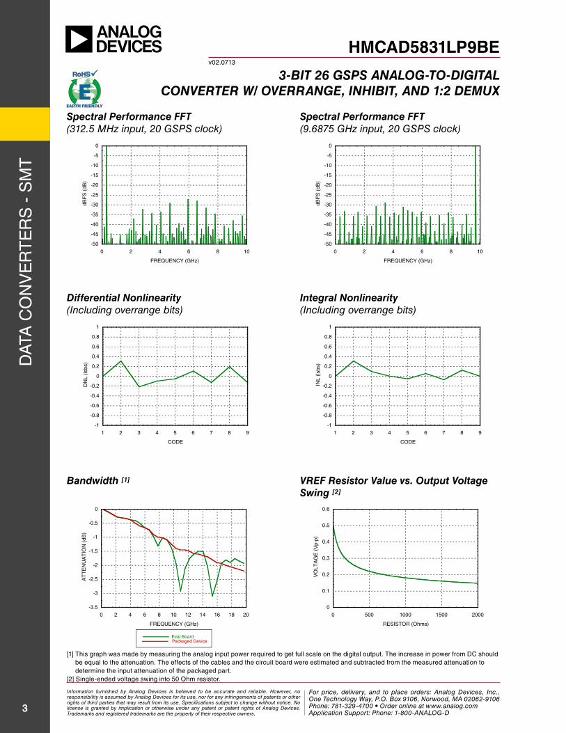
Bandwidth [1]
Integral Nonlinearity(Including overrange bits)
Differential Nonlinearity(Including overrange bits)
Spectral Performance FFT(9.6875 GHz input, 20 GSPS clock)
Spectral Performance FFT(312.5 MHz input, 20 GSPS clock)
[1] this graph was made by measuring the analog input power required to get full scale on the digital output. the increase in power from DC should be equal to the attenuation. the effects of the cables and the circuit board were estimated and subtracted from the measured attenuation to determine the input attenuation of the packaged part.
[2] single-ended voltage swing into 50 ohm resistor.
VREF Resistor Value vs. Output Voltage Swing [2]
-50
-45
-40
-35
-30
-25
-20
-15
-10
-5
0
0 2 4 6 8 10
dBF
S (
dB)
FREQUENCY (GHz)
-50
-45
-40
-35
-30
-25
-20
-15
-10
-5
0
0 2 4 6 8 10
dBF
S (
dB)
FREQUENCY (GHz)
-1
-0.8
-0.6
-0.4
-0.2
0
0.2
0.4
0.6
0.8
1
1 2 3 4 5 6 7 8 9
DN
L (ls
bs)
CODE
-1
-0.8
-0.6
-0.4
-0.2
0
0.2
0.4
0.6
0.8
1
1 2 3 4 5 6 7 8 9
INL
(lsbs
)
CODE
-3.5
-3
-2.5
-2
-1.5
-1
-0.5
0
0 2 4 6 8 10 12 14 16 18 20
Eval Board Packaged Device
AT
TE
NU
AT
ION
(dB
)
FREQUENCY (GHz)
0
0.1
0.2
0.3
0.4
0.5
0.6
0 500 1000 1500 2000
VO
LTA
GE
(V
p-p)
RESISTOR (Ohms)
Information furnished by Analog Devices is believed to be accurate and reliable. However, no responsibility is assumed by Analog Devices for its use, nor for any infringements of patents or other rights of third parties that may result from its use. Specifications subject to change without notice. No license is granted by implication or otherwise under any patent or patent rights of Analog Devices. Trademarks and registered trademarks are the property of their respective owners.
For price, delivery, and to place orders: Analog Devices, Inc., One Technology Way, P.O. Box 9106, Norwood, MA 02062-9106 Phone: 781-329-4700 • Order online at www.analog.com Application Support: Phone: 1-800-ANALOG-D
For price, delivery and to place orders: Hittite Microwave Corporation, 2 Elizabeth Drive, Chelmsford, MA 01824Phone: 978-250-3343 Fax: 978-250-3373 Order On-line at www.hittite.com
Application Support: Phone: 978-250-3343 or [email protected]
Dat
a C
on
ve
rt
er
s -
sM
t
4
HMCAD5831LP9BEv02.0713
3-BIT 26 GSPS ANALOG-TO-DIGITALCONVERTER W/ OVERRANGE, INHIBIT, AND 1:2 DEMUX
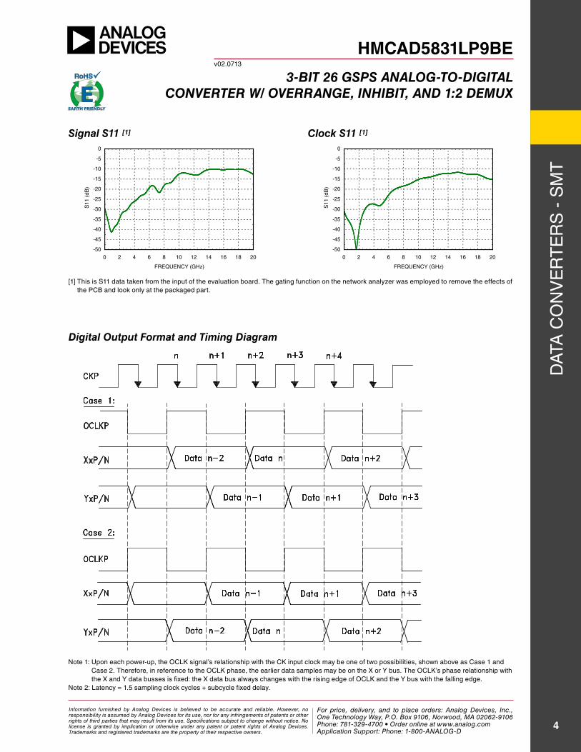
Clock S11 [1]Signal S11 [1]
Digital Output Format and Timing Diagram
[1] this is s11 data taken from the input of the evaluation board. the gating function on the network analyzer was employed to remove the effects of the PCB and look only at the packaged part.
-50
-45
-40
-35
-30
-25
-20
-15
-10
-5
0
0 2 4 6 8 10 12 14 16 18 20
S11
(dB
)
FREQUENCY (GHz)
-50
-45
-40
-35
-30
-25
-20
-15
-10
-5
0
0 2 4 6 8 10 12 14 16 18 20
S11
(dB
)
FREQUENCY (GHz)
note 1: Upon each power-up, the oCLK signal’s relationship with the CK input clock may be one of two possibilities, shown above as Case 1 and Case 2. therefore, in reference to the oCLK phase, the earlier data samples may be on the X or Y bus. the oCLK’s phase relationship with the X and Y data busses is fixed: the X data bus always changes with the rising edge of oCLK and the Y bus with the falling edge.
note 2: Latency = 1.5 sampling clock cycles + subcycle fixed delay.
Information furnished by Analog Devices is believed to be accurate and reliable. However, no responsibility is assumed by Analog Devices for its use, nor for any infringements of patents or other rights of third parties that may result from its use. Specifications subject to change without notice. No license is granted by implication or otherwise under any patent or patent rights of Analog Devices. Trademarks and registered trademarks are the property of their respective owners.
For price, delivery, and to place orders: Analog Devices, Inc., One Technology Way, P.O. Box 9106, Norwood, MA 02062-9106 Phone: 781-329-4700 • Order online at www.analog.com Application Support: Phone: 1-800-ANALOG-D
For price, delivery and to place orders: Hittite Microwave Corporation, 2 Elizabeth Drive, Chelmsford, MA 01824Phone: 978-250-3343 Fax: 978-250-3373 Order On-line at www.hittite.com
Application Support: Phone: 978-250-3343 or [email protected]
Dat
a C
on
ve
rt
er
s -
sM
t
5
HMCAD5831LP9BEv02.0713
3-BIT 26 GSPS ANALOG-TO-DIGITALCONVERTER W/ OVERRANGE, INHIBIT, AND 1:2 DEMUX
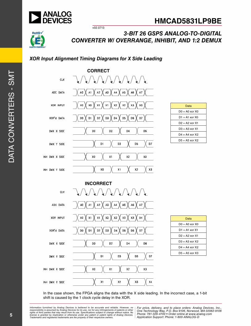
XOR Input Alignment Timing Diagrams for X Side Leading
Data
D0 = a0 xor X0
D1 = a1 xor X0
D2 = a2 xor X1
D3 = a3 xor X1
D4 = a4 xor X2
D5 = a5 xor X2
CORRECT
Data
D0 = a0 xor X0
D1 = a1 xor X1
D2 = a2 xor X1
D3 = a3 xor X2
D4 = a4 xor X2
D5 = a5 xor X3
In the case shown, the FPGa aligns the data with the X side leading. In the incorrect case, a 1-bit shift is caused by the 1 clock cycle delay in the Xor.
INCORRECT
Information furnished by Analog Devices is believed to be accurate and reliable. However, no responsibility is assumed by Analog Devices for its use, nor for any infringements of patents or other rights of third parties that may result from its use. Specifications subject to change without notice. No license is granted by implication or otherwise under any patent or patent rights of Analog Devices. Trademarks and registered trademarks are the property of their respective owners.
For price, delivery, and to place orders: Analog Devices, Inc., One Technology Way, P.O. Box 9106, Norwood, MA 02062-9106 Phone: 781-329-4700 • Order online at www.analog.com Application Support: Phone: 1-800-ANALOG-D
For price, delivery and to place orders: Hittite Microwave Corporation, 2 Elizabeth Drive, Chelmsford, MA 01824Phone: 978-250-3343 Fax: 978-250-3373 Order On-line at www.hittite.com
Application Support: Phone: 978-250-3343 or [email protected]
Dat
a C
on
ve
rt
er
s -
sM
t
6
HMCAD5831LP9BEv02.0713
3-BIT 26 GSPS ANALOG-TO-DIGITALCONVERTER W/ OVERRANGE, INHIBIT, AND 1:2 DEMUX
Parameter Description Min. typ. Max. Units
aveeanalog supply voltage range -5.5 -5.0 -4.5 v
oveeDigital and output driver supply voltage range -3.6 -3.3 -3.0 v
vinputIn, CKx, Xorx, and Qtx inputs voltage -2.0 +0.5 v
voutputXxx, Yxx, and oCLKx outputs voltage -1.5 +0.5 v
aGnD-oGnD -0.3 0 +0.3 v
ta
ambient temperatureLimited by the Absolute Maximum junction temperature
limit and depends upon the system thermal design-40 +85 °C
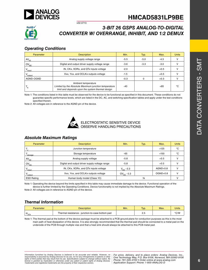
Absolute Maximum Ratings
eLeCtrostatIC sensItIve DevICeoBserve HanDLInG PreCaUtIons
Operating Conditions
note 1: the conditions listed in this table must be observed for the device to be functional as specified in this document. these conditions do not guarantee specific performance levels, which are listed in the DC, aC, and switching specification tables and apply under the test conditions specified therein.
note 2: all voltages are in reference to the aGnD pin of the device.
Parameter Description Min. typ. Max. Units
tJJunction temperature +125 °C
tstoragestorage temperature -65 +150 °C
aveeanalog supply voltage -5.8 +0.5 v
oveeDigital and output driver supply voltage range -5.8 +0.5 v
vinputIn, CKx, Xorx, and Qtx inputs voltage vee - 0.3 aGnD+0.8 v
voutputXxx, Yxx, and oCLKx outputs voltage ovee - 0.3 oGnD+0.8 v
esD rating Human body model (Class 1C) 1k v
note 1: operating the device beyond the limits specified in this table may cause immediate damage to the device. Functional operation of the device is further limited by the operating Conditions. Device functionality is not implied by the absolute Maximum ratings.
note 2: all voltages are in reference to aGnD pin of the device.
Thermal InformationParameter Description Min. typ. Max. Units
ΘJCbthermal resistance - junction-to-case bottom pad 2.5 °C/W
note 1: the thermal pad at the bottom of the device package must be attached to a PCB ground plane for conduction purposes as this is the most main path of heat dissipation of this device. It is also strongly recommended that the thermal pad should be connected to a metal pad on the underside of the PCB through multiple vias and that a heat sink should always be attached to this PCB metal pad.
Information furnished by Analog Devices is believed to be accurate and reliable. However, no responsibility is assumed by Analog Devices for its use, nor for any infringements of patents or other rights of third parties that may result from its use. Specifications subject to change without notice. No license is granted by implication or otherwise under any patent or patent rights of Analog Devices. Trademarks and registered trademarks are the property of their respective owners.
For price, delivery, and to place orders: Analog Devices, Inc., One Technology Way, P.O. Box 9106, Norwood, MA 02062-9106 Phone: 781-329-4700 • Order online at www.analog.com Application Support: Phone: 1-800-ANALOG-D
For price, delivery and to place orders: Hittite Microwave Corporation, 2 Elizabeth Drive, Chelmsford, MA 01824Phone: 978-250-3343 Fax: 978-250-3373 Order On-line at www.hittite.com
Application Support: Phone: 978-250-3343 or [email protected]
Dat
a C
on
ve
rt
er
s -
sM
t
7
HMCAD5831LP9BEv02.0713
3-BIT 26 GSPS ANALOG-TO-DIGITALCONVERTER W/ OVERRANGE, INHIBIT, AND 1:2 DEMUX
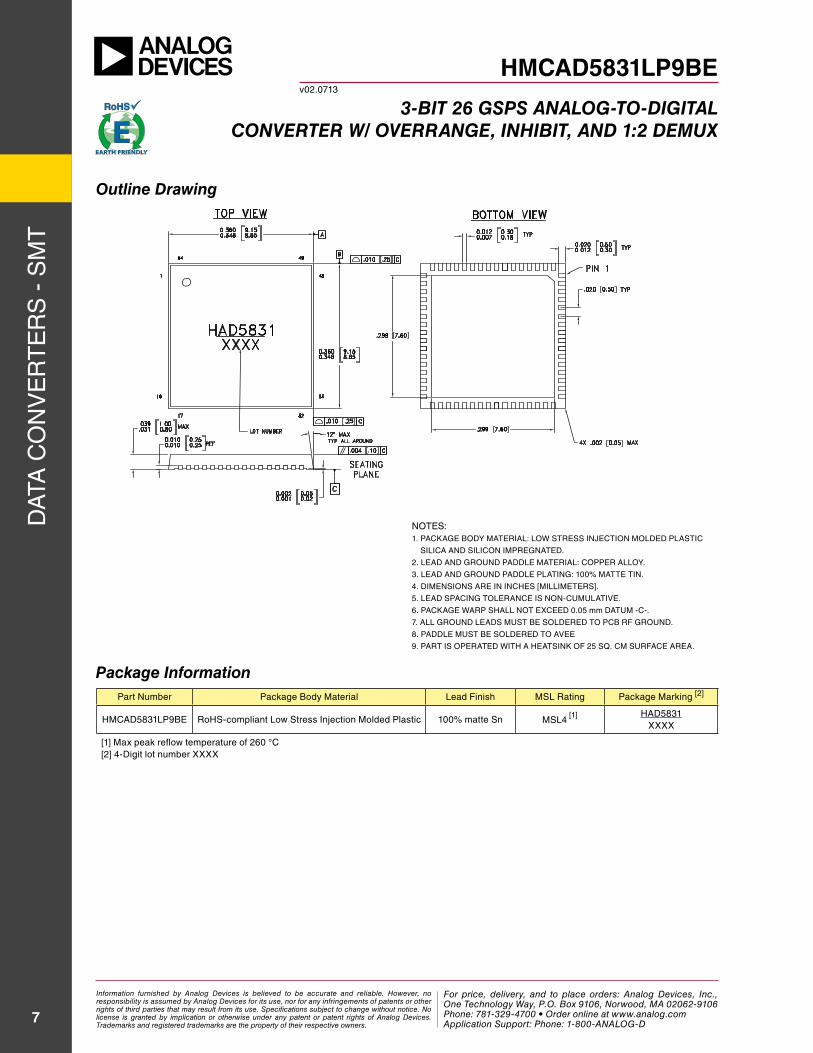
Outline Drawing
notes:1. PaCKaGe BoDY MaterIaL: LoW stress InJeCtIon MoLDeD PLastIC
sILICa anD sILICon IMPreGnateD.
2. LeaD anD GroUnD PaDDLe MaterIaL: CoPPer aLLoY.
3. LeaD anD GroUnD PaDDLe PLatInG: 100% Matte tIn.
4. DIMensIons are In InCHes [MILLIMeters].
5. LeaD sPaCInG toLeranCe Is non-CUMULatIve.
6. PaCKaGe WarP sHaLL not eXCeeD 0.05 mm DatUM -C-.
7. aLL GroUnD LeaDs MUst Be soLDereD to PCB rF GroUnD.
8. PaDDLe MUst Be soLDereD to avee
9. Part Is oPerateD WItH a HeatsInK oF 25 sQ. CM sUrFaCe area.
Part number Package Body Material Lead Finish MsL rating Package Marking [2]
HMCaD5831LP9Be roHs-compliant Low stress Injection Molded Plastic 100% matte sn MsL4 [1] HaD5831
XXXX
[1] Max peak reflow temperature of 260 °C[2] 4-Digit lot number XXXX
Package Information
Information furnished by Analog Devices is believed to be accurate and reliable. However, no responsibility is assumed by Analog Devices for its use, nor for any infringements of patents or other rights of third parties that may result from its use. Specifications subject to change without notice. No license is granted by implication or otherwise under any patent or patent rights of Analog Devices. Trademarks and registered trademarks are the property of their respective owners.
For price, delivery, and to place orders: Analog Devices, Inc., One Technology Way, P.O. Box 9106, Norwood, MA 02062-9106 Phone: 781-329-4700 • Order online at www.analog.com Application Support: Phone: 1-800-ANALOG-D
For price, delivery and to place orders: Hittite Microwave Corporation, 2 Elizabeth Drive, Chelmsford, MA 01824Phone: 978-250-3343 Fax: 978-250-3373 Order On-line at www.hittite.com
Application Support: Phone: 978-250-3343 or [email protected]
Dat
a C
on
ve
rt
er
s -
sM
t
8
HMCAD5831LP9BEv02.0713
3-BIT 26 GSPS ANALOG-TO-DIGITALCONVERTER W/ OVERRANGE, INHIBIT, AND 1:2 DEMUX
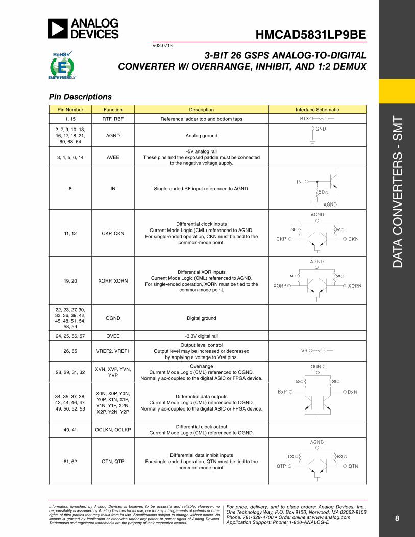
Pin DescriptionsPin number Function Description Interface schematic
1, 15 rtF, rBF reference ladder top and bottom taps
2, 7, 9, 10, 13, 16, 17, 18, 21,
60, 63, 64aGnD analog ground
3, 4, 5, 6, 14 avee-5v analog rail
these pins and the exposed paddle must be connected to the negative voltage supply.
8 In single-ended rF input referenced to aGnD.
11, 12 CKP, CKn
Differential clock inputsCurrent Mode Logic (CML) referenced to aGnD.
For single-ended operation, CKn must be tied to the common-mode point.
19, 20 XorP, Xorn
Differential Xor inputsCurrent Mode Logic (CML) referenced to aGnD.
For single-ended operation, Xorn must be tied to the common-mode point.
22, 23, 27, 30, 33, 36, 39, 42, 45, 48, 51, 54,
58, 59
oGnD Digital ground
24, 25, 56, 57 ovee -3.3v digital rail
26, 55 vreF2, vreF1output level control
output level may be increased or decreased by applying a voltage to vref pins.
28, 29, 31, 32Xvn, XvP, Yvn,
YvP
overrangeCurrent Mode Logic (CML) referenced to oGnD.
normally ac-coupled to the digital asIC or FPGa device.
34, 35, 37, 38, 43, 44, 46, 47, 49, 50, 52, 53
X0n, X0P, Y0n, Y0P, X1n, X1P, Y1n, Y1P, X2n, X2P, Y2n, Y2P
Differential data outputsCurrent Mode Logic (CML) referenced to oGnD.
normally ac-coupled to the digital asIC or FPGa device.
40, 41 oCLKn, oCLKPDifferential clock output
Current Mode Logic (CML) referenced to oGnD.
61, 62 Qtn, QtPDifferential data inhibit inputs
For single-ended operation, Qtn must be tied to the common-mode point.
Information furnished by Analog Devices is believed to be accurate and reliable. However, no responsibility is assumed by Analog Devices for its use, nor for any infringements of patents or other rights of third parties that may result from its use. Specifications subject to change without notice. No license is granted by implication or otherwise under any patent or patent rights of Analog Devices. Trademarks and registered trademarks are the property of their respective owners.
For price, delivery, and to place orders: Analog Devices, Inc., One Technology Way, P.O. Box 9106, Norwood, MA 02062-9106 Phone: 781-329-4700 • Order online at www.analog.com Application Support: Phone: 1-800-ANALOG-D
For price, delivery and to place orders: Hittite Microwave Corporation, 2 Elizabeth Drive, Chelmsford, MA 01824Phone: 978-250-3343 Fax: 978-250-3373 Order On-line at www.hittite.com
Application Support: Phone: 978-250-3343 or [email protected]
Dat
a C
on
ve
rt
er
s -
sM
t
9
HMCAD5831LP9BEv02.0713
3-BIT 26 GSPS ANALOG-TO-DIGITALCONVERTER W/ OVERRANGE, INHIBIT, AND 1:2 DEMUX
the aDC’s voltage reference ladder comprises 8, 18 Ω resistors, or 144 Ω total nominal resistance. Pin 1, rtF, and pin 15, rBF, are provided for the top and bottom reference taps. these pins are driven by external supplies to establish the desired full-scale range of the aDC. the rF signal input (pin 8, In) to the aDC, which is nominally centered at 0v (aGnD), drives an internal emitter follower with a nominal vBe of -936 mv. Hence the center of full-scale range should center near -936 mv. the voltage at pin rtF is then -936 mv + vfull-scale/2. Likewise the voltage at pin rBF is -936 mv - vfull-scale/2.
as an example, if the user had a peak-to-peak input voltage swing of 256 mv centered at 0v and required the full-scale input range of the aDC to be 256 mv as well, rtF would be -936 mv + 128 mv = -772 mv. rBF would be -936 mv - 128 mv = -1.028v. note that the diode drop, -936 mv, is dependent on temperature and process variations. rtF and rBF values in the “electrical specifications” table on pages 1 and 2 are shown as nominal values only.
the rF input is internally terminated with 50 ohms to aGnD, which should be the system rF ground. normally, the input signal is expected to have a common-mode point at this 0v point. Because this device allows the user to set the top and bottom voltages of the reference ladder inside the device, the user has significant flexibility in adjusting the aDC span and thus the full-scale signal amplitude as well as the input signal’s common-mode point.
However, it is very important to notice that there are absolute voltage level limits on the peak input signal voltage. these are indicated in the operating Conditions table in this document. For proper operation of the device, the input signal must never swing higher than the vinput-max or lower than vinput-min voltages indicated in the operating Conditions table.
the user is cautioned to also pay attention to the absolute Maximum ratings table as it lists the maximum input voltage beyond which damage to the device will result.
Reference Ladder
Application Information
Input Signal
VREF PinsPins 26 and 55 (vreF1 and vreF2) should be connected together off chip and the pair is then connected to the oGnD through a resistor. these pins are used to vary the output swing voltage. the application Circuit shown uses a 200 Ω resistor. this provides the typical output swings listed in the electrical specifications table. Increasing the voltage on vreF1 and vreF2 will increase the output swing. Conversely, decreasing the vreF1 and vreF2 voltages will decrease the output swing.
Overrange OutputPins 28, 29, 31, and 32 provide overrange output bits. this function indicates when the input signal is out of range of the reference ladder voltages. the bit will be high when either the signal is above rtF or below rBF. the overrange bit is cleared for the next clock cycle containing in-range data.
Data Inhibitall data outputs can be forced to “0” by enabling the Data Inhibit function (pins 61 and 62). By driving the QtP pin high and the Qtn pin low, the aDC core will produce all 0s. this occurs prior to the Xor function and the demux. When QtP is low and Qtn is high, the chip operates normally, and these inputs must be set this way for normal operation.
Information furnished by Analog Devices is believed to be accurate and reliable. However, no responsibility is assumed by Analog Devices for its use, nor for any infringements of patents or other rights of third parties that may result from its use. Specifications subject to change without notice. No license is granted by implication or otherwise under any patent or patent rights of Analog Devices. Trademarks and registered trademarks are the property of their respective owners.
For price, delivery, and to place orders: Analog Devices, Inc., One Technology Way, P.O. Box 9106, Norwood, MA 02062-9106 Phone: 781-329-4700 • Order online at www.analog.com Application Support: Phone: 1-800-ANALOG-D
For price, delivery and to place orders: Hittite Microwave Corporation, 2 Elizabeth Drive, Chelmsford, MA 01824Phone: 978-250-3343 Fax: 978-250-3373 Order On-line at www.hittite.com
Application Support: Phone: 978-250-3343 or [email protected]
Dat
a C
on
ve
rt
er
s -
sM
t
10
HMCAD5831LP9BEv02.0713
3-BIT 26 GSPS ANALOG-TO-DIGITALCONVERTER W/ OVERRANGE, INHIBIT, AND 1:2 DEMUX
Data XORall data outputs from the aDC core can be modulated by an external source. this allows the user to use aC coupling for output line connection to a serDes input of an FPGa. this function occurs prior to the demux. the Xor input signal is retimed by the full rate internal clock and requires low jitter and suitable rise and fall times. Please contact Hittite Microwave for sample driver circuits. typical modulation frequencies are 100 MHz to 300 MHz. For a square wave signal, a multiple of two divisor of the full rate internal clock should be used, e.g. 1/128th or 1/64th of the aDC clock. Due to the nature of the retiming scheme, the demux channel relationship timing can vary. this is dependent on when the Xor input is sampled relative to the full rate internal clock. see timing diagrams on page 5. For example, a nominal setup may have demux side X leading and side Y trailing. If the Xor input is shifted relative to the internal clock, side Y may lead and side X may trail. It is highly recommended that a variable delay be used to adjust the phase of the Xor input to avoid transitions that are very close to internal clock edges. see typical operation example for more information. the Xor function can be used with the Data Inhibit function to produce a sync pattern for aligning the lanes of serDes inputs. the device outputs are inverted when Xor is low.
Application Information (continued)
Evaluation Board DescriptionevaL01-HMC5831LP9 (131498-3) demonstrates the HMCaD5831LP9Be in an environment ready to be connected to an FPGa. along with the aDC, the board features three other Hittite Microwave components. the clock output of the aDC is divided down by 32 (a stage of 8 and a stage of 4, U1, and U2) to produce a clock output that is 1/64th of the aDC clock input. this clock is available to drive the FPGa or other system components. the aDC Xor input has programmable delay (U4) allowing the user to fine-tune the Xor clock edges going into the aDC. the InHIBIt and D8BX inputs are 0 to +3.3v, compatible with most FPGas. Finally, the aDC_vr pin allows the user to control the output voltage swing of the aDC. output connectors J2 and J3 are high-performance saMteC connectors, part number erF8-013-05.0-Dv.
Ten-Level Operationthe HMCaD5831LP9Be can be used as a ten-level (3.32 bits) aDC by combining the regular data outputs with the overrange Bit. the bottom code (code 0) is equal to ovr high and all the bits low. For codes 1 through 8, the aDC functions normally (with ovr low). the top code, code 9, is all bits high. note that the InL/DnL plots include ovr in this manner.
Information furnished by Analog Devices is believed to be accurate and reliable. However, no responsibility is assumed by Analog Devices for its use, nor for any infringements of patents or other rights of third parties that may result from its use. Specifications subject to change without notice. No license is granted by implication or otherwise under any patent or patent rights of Analog Devices. Trademarks and registered trademarks are the property of their respective owners.
For price, delivery, and to place orders: Analog Devices, Inc., One Technology Way, P.O. Box 9106, Norwood, MA 02062-9106 Phone: 781-329-4700 • Order online at www.analog.com Application Support: Phone: 1-800-ANALOG-D
For price, delivery and to place orders: Hittite Microwave Corporation, 2 Elizabeth Drive, Chelmsford, MA 01824Phone: 978-250-3343 Fax: 978-250-3373 Order On-line at www.hittite.com
Application Support: Phone: 978-250-3343 or [email protected]
Dat
a C
on
ve
rt
er
s -
sM
t
11
HMCAD5831LP9BEv02.0713
3-BIT 26 GSPS ANALOG-TO-DIGITALCONVERTER W/ OVERRANGE, INHIBIT, AND 1:2 DEMUX
Operation Over Full Temperature Range
Application Information (continued)
the device typically consumes 4.2 watts power and thus requires careful thermal design at the system level. a heat sink of at least 25 cm^2 surface area is required under all conditions. Most of the device heat dissipation occurs on the bottom side of the package. the package has a thermal paddle on the bottom side. the PCB design must solder this paddle through a grid of several thermal vias to a metal pad on the bottom side of the PCB where the heat sink should be attached. In addition, the avee pins of the device and the paddle must be connected to the negative -5v supply plane. It is highly recommended that some manner of additional cooling technique should be employed in order to maximize the ambient temperature range of the device’s operation.
the electrical specifications section lists only the performance parameters at +25 °C temperature. the performance diminishes as temperature increases. on the device evaluation board, in Hittite lab settings with minimal air flow, a temperature rise of 18-20 °C was observed between the ambient temperature and the thermal pad at the bottom of the PCB. the ultimate limit to the device’s temperature capabilities is the maximum junction temperature specified in the absolute Maximum ratings table in this document. the thermal resistance from the device junction to the device thermal paddle is specified in the thermal Information table. With this information and knowledge of the system’s heat dissipation capabilities from the PCB pad to the ambient, one can determine the ambient temperature range the device can support.
Based on data taken on the device evaluation board under Hittite’s lab conditions, it is believed that 22 Gs/s maximum speed can be expected across the temperature range of -40 °C and +85 °C with reasonable system thermal design.
Typical Operation ExampleWhen using the device evaluation board, high-quality signal generator equipment must be used that provides low enough broadband phase noise to support the snr specifications of this device at the very high signal frequencies.
the reference ladder voltages should be provided with stable, linear power supplies. as a starting point, it is recommended that the rtF and rBF voltage should be set to -772 mv and -1.028v, as described in the reference Ladder subsection. the input signal can then be provided with the appropriate signal generator with 50 ohm, single-ended output that is ac-coupled into the eval board’s sMa connector. the signal generator output strength should be set at a low level such as -20 dBm before the output is enabled. the signal level can then be increased gradually as required, but never beyond the 256 mv full-scale swing that had been selected in this example. the Clock input can similarly be provided with an rF signal generator or a Hittite PLL/vCo device evaluation board, provided that the CKn input is set at the common-mode point – 0 v (aGnD) in this case. although higher amplitudes are possible, initially the user should keep the clock signal strength at -3 dBm or less. and, of course, care should be taken with the clock input as well to not overload the aDC.
an FPGa with suitably fast serDes inputs can capture data from the HMCaD5831LP9Be using the following routine. the FPGa produces an InHIBIt high signal causing the aDC core to produce all 0s. the Xor input to the aDC runs at a slow clock rate and modulates the aDC output to produce a known waveform at the FPGa inputs. the FPGa then uses these signals to align the lanes. When the lanes are aligned, the InHIBIt signal goes low and the aDC produces signal data that continues to be modulated by the Xor input. the FPGa then corrects for the modulation. note that the FPGa can generate the Xor modulation signal (in which case a PrBs sequence could be used). Depending on the phase of the Xor input modulation waveform, either demux output (X or Y) can be the leading data sample. In this case, the FPGa would need to resolve which lane is the leader. this can be accomplished by driving the aDC with a known signal, evaluating the outputs and reassembling FPGa data if necessary. It is recommended to do this on each power-up. It is also recommended to perform a routine to ensure that the Xor input waveform is properly aligned with the internal clock. this can be accomplished by sweeping the external variable delay stage.
Information furnished by Analog Devices is believed to be accurate and reliable. However, no responsibility is assumed by Analog Devices for its use, nor for any infringements of patents or other rights of third parties that may result from its use. Specifications subject to change without notice. No license is granted by implication or otherwise under any patent or patent rights of Analog Devices. Trademarks and registered trademarks are the property of their respective owners.
For price, delivery, and to place orders: Analog Devices, Inc., One Technology Way, P.O. Box 9106, Norwood, MA 02062-9106 Phone: 781-329-4700 • Order online at www.analog.com Application Support: Phone: 1-800-ANALOG-D
For price, delivery and to place orders: Hittite Microwave Corporation, 2 Elizabeth Drive, Chelmsford, MA 01824Phone: 978-250-3343 Fax: 978-250-3373 Order On-line at www.hittite.com
Application Support: Phone: 978-250-3343 or [email protected]
Dat
a C
on
ve
rt
er
s -
sM
t
12
HMCAD5831LP9BEv02.0713
3-BIT 26 GSPS ANALOG-TO-DIGITALCONVERTER W/ OVERRANGE, INHIBIT, AND 1:2 DEMUX
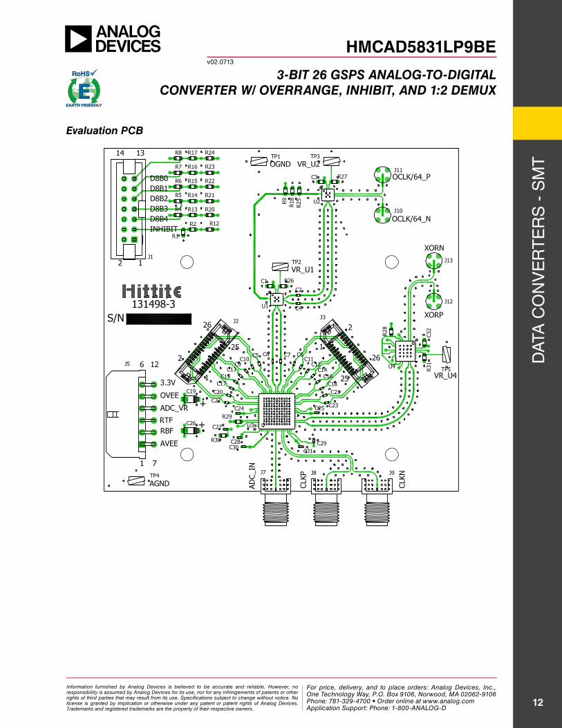
Evaluation PCB
Information furnished by Analog Devices is believed to be accurate and reliable. However, no responsibility is assumed by Analog Devices for its use, nor for any infringements of patents or other rights of third parties that may result from its use. Specifications subject to change without notice. No license is granted by implication or otherwise under any patent or patent rights of Analog Devices. Trademarks and registered trademarks are the property of their respective owners.
For price, delivery, and to place orders: Analog Devices, Inc., One Technology Way, P.O. Box 9106, Norwood, MA 02062-9106 Phone: 781-329-4700 • Order online at www.analog.com Application Support: Phone: 1-800-ANALOG-D
For price, delivery and to place orders: Hittite Microwave Corporation, 2 Elizabeth Drive, Chelmsford, MA 01824Phone: 978-250-3343 Fax: 978-250-3373 Order On-line at www.hittite.com
Application Support: Phone: 978-250-3343 or [email protected]
Dat
a C
on
ve
rt
er
s -
sM
t
13
HMCAD5831LP9BEv02.0713
3-BIT 26 GSPS ANALOG-TO-DIGITALCONVERTER W/ OVERRANGE, INHIBIT, AND 1:2 DEMUX
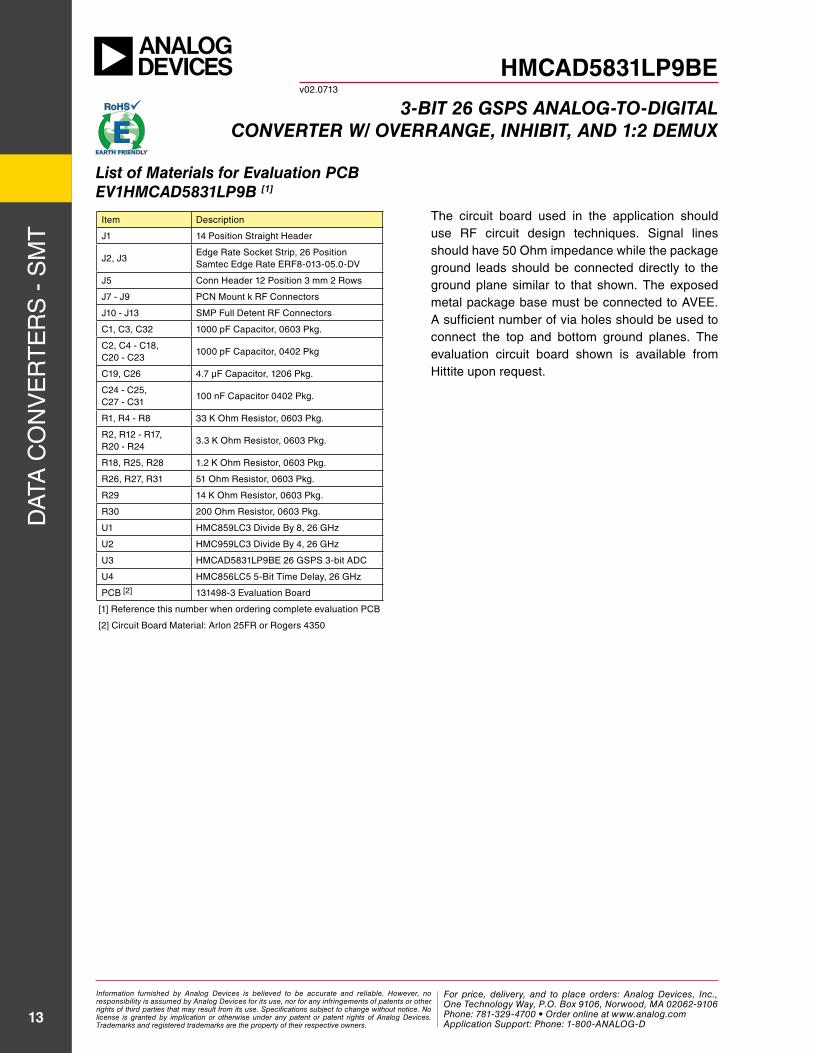
List of Materials for Evaluation PCB EV1HMCAD5831LP9B [1]
Item Description
J1 14 Position straight Header
J2, J3edge rate socket strip, 26 Positionsamtec edge rate erF8-013-05.0-Dv
J5 Conn Header 12 Position 3 mm 2 rows
J7 - J9 PCn Mount k rF Connectors
J10 - J13 sMP Full Detent rF Connectors
C1, C3, C32 1000 pF Capacitor, 0603 Pkg.
C2, C4 - C18, C20 - C23
1000 pF Capacitor, 0402 Pkg
C19, C26 4.7 µF Capacitor, 1206 Pkg.
C24 - C25, C27 - C31
100 nF Capacitor 0402 Pkg.
r1, r4 - r8 33 K ohm resistor, 0603 Pkg.
r2, r12 - r17, r20 - r24
3.3 K ohm resistor, 0603 Pkg.
r18, r25, r28 1.2 K ohm resistor, 0603 Pkg.
r26, r27, r31 51 ohm resistor, 0603 Pkg.
r29 14 K ohm resistor, 0603 Pkg.
r30 200 ohm resistor, 0603 Pkg.
U1 HMC859LC3 Divide By 8, 26 GHz
U2 HMC959LC3 Divide By 4, 26 GHz
U3 HMCaD5831LP9Be 26 GsPs 3-bit aDC
U4 HMC856LC5 5-Bit time Delay, 26 GHz
PCB [2] 131498-3 evaluation Board
[1] reference this number when ordering complete evaluation PCB
[2] Circuit Board Material: arlon 25Fr or rogers 4350
the circuit board used in the application should use rF circuit design techniques. signal lines should have 50 ohm impedance while the package ground leads should be connected directly to the ground plane similar to that shown. the exposed metal package base must be connected to avee. a sufficient number of via holes should be used to connect the top and bottom ground planes. the evaluation circuit board shown is available from Hittite upon request.
Information furnished by Analog Devices is believed to be accurate and reliable. However, no responsibility is assumed by Analog Devices for its use, nor for any infringements of patents or other rights of third parties that may result from its use. Specifications subject to change without notice. No license is granted by implication or otherwise under any patent or patent rights of Analog Devices. Trademarks and registered trademarks are the property of their respective owners.
For price, delivery, and to place orders: Analog Devices, Inc., One Technology Way, P.O. Box 9106, Norwood, MA 02062-9106 Phone: 781-329-4700 • Order online at www.analog.com Application Support: Phone: 1-800-ANALOG-D
For price, delivery and to place orders: Hittite Microwave Corporation, 2 Elizabeth Drive, Chelmsford, MA 01824Phone: 978-250-3343 Fax: 978-250-3373 Order On-line at www.hittite.com
Application Support: Phone: 978-250-3343 or [email protected]
Dat
a C
on
ve
rt
er
s -
sM
t
14
HMCAD5831LP9BEv02.0713
3-BIT 26 GSPS ANALOG-TO-DIGITALCONVERTER W/ OVERRANGE, INHIBIT, AND 1:2 DEMUX
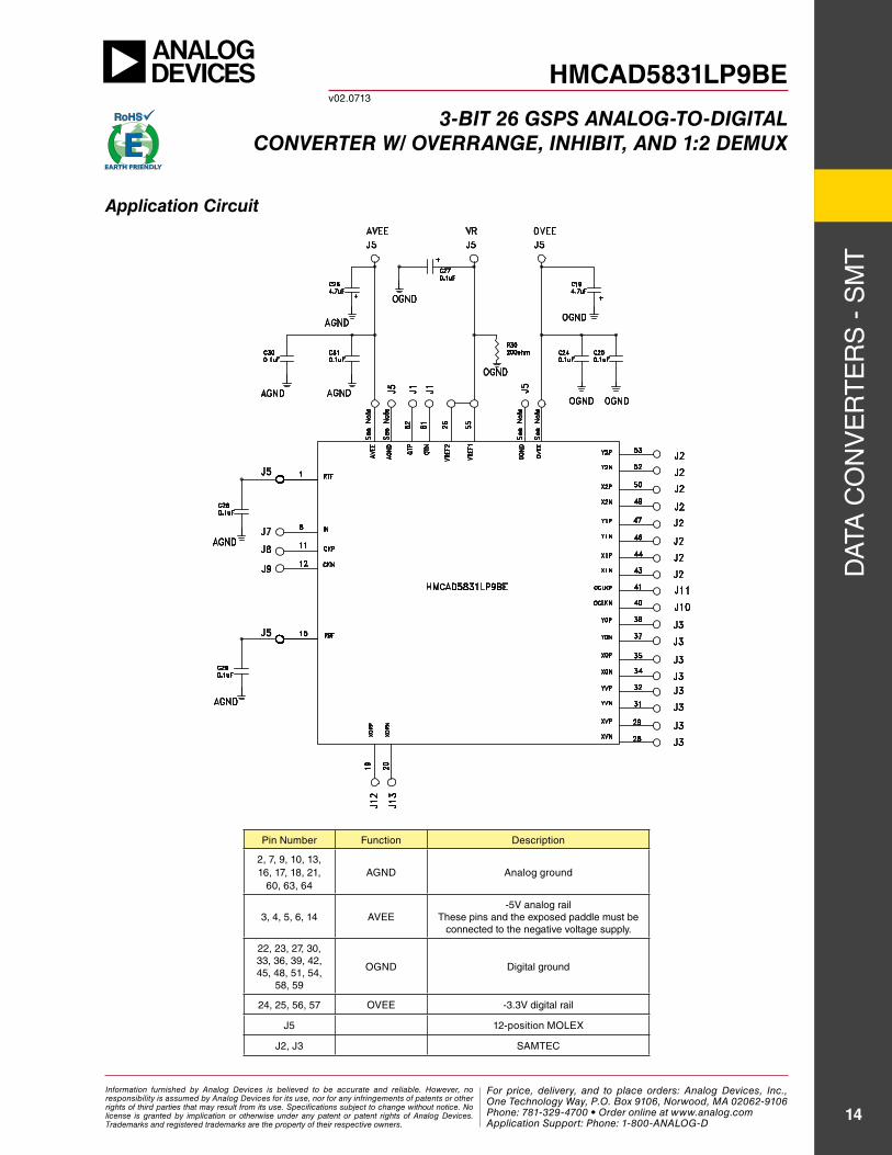
Application Circuit
Pin number Function Description
2, 7, 9, 10, 13, 16, 17, 18, 21,
60, 63, 64aGnD analog ground
3, 4, 5, 6, 14 avee-5v analog rail
these pins and the exposed paddle must be connected to the negative voltage supply.
22, 23, 27, 30, 33, 36, 39, 42, 45, 48, 51, 54,
58, 59
oGnD Digital ground
24, 25, 56, 57 ovee -3.3v digital rail
J5 12-position MoLeX
J2, J3 saMteC
Information furnished by Analog Devices is believed to be accurate and reliable. However, no responsibility is assumed by Analog Devices for its use, nor for any infringements of patents or other rights of third parties that may result from its use. Specifications subject to change without notice. No license is granted by implication or otherwise under any patent or patent rights of Analog Devices. Trademarks and registered trademarks are the property of their respective owners.
For price, delivery, and to place orders: Analog Devices, Inc., One Technology Way, P.O. Box 9106, Norwood, MA 02062-9106 Phone: 781-329-4700 • Order online at www.analog.com Application Support: Phone: 1-800-ANALOG-D