A 6b 1.6GS/s ADC with Redundant Cycle 1-Tap Embedded DFE...
4
Channel TX M U X ADC DSP N bits Fig. 1. A high-speed link with an ADC-based receiver. V in α ADC Z -1 n bits MSB m bits V in Digital DFE Embedded DFE Z -1 α Σ Σ ADC n bits MSB Fig. 2. Block diagrams of digital and embedded DFE. A 6b 1.6GS/s ADC with Redundant Cycle 1-Tap Embedded DFE in 90nm CMOS E. Zhian Tabasy, A. Shafik, S. Huang, N. Yang, S. Hoyos, and S. Palermo Texas A&M University, College Station, TX 77843 Abstract-Serial link receivers with ADC front-ends are emerging in order to scale data rates over high attenuation channels. Embedding partial equalization inside the front-end ADC can potentially result in lowering the complexity of back-end DSP and/or decreasing the ADC resolution requirement, which results in a more energy-efficient receiver. This paper presents a 6b 1.6GS/s ADC with a novel embedded DFE structure. Leveraging a time-interleaved SAR ADC architecture, a redundant cycle loop-unrolled technique is proposed in order to relax the DFE feedback critical path delay with low power/area overhead. Fabricated in an LP 90nm CMOS process, the 6b ADC with embedded 1-tap DFE consumes 20mW total power, including front-end T/Hs and reference buffers, and the core time- interleaved ADC occupies 0.24mm 2 area. I. INTRODUCTION Serial link receivers with analog-to-digital (ADC) front- ends are being proposed in order to increase data rates over high-loss channels [1]. Fig. 1 shows a block diagram of a high-speed link employing an ADC-based receiver which feeds a DSP block. The performance of this DSP block scales with improved CMOS technology, allowing for the efficient implementation of complex equalization and symbol detection schemes. However, improvements in the power efficiency of the high-sample rate ADC and also the subsequent digital processing are necessary to support future high bandwidth systems. Embedding partial analog equalization in the front- end ADC allows for both a lower ADC resolution and reduced digital equalization complexity at a target bit-error rate (BER) [2], which could translate into an overall lower-power ADC- based receiver implementation. Schemes to implement embedded multi-level decision- feedback equalization (DFE) have been proposed for pipeline ADC architectures [3]. An important issue in any DFE architecture involves closing timing on the critical feedback path from the decision comparator to the summation circuit, which subtracts the post-cursor inter-symbol interference (ISI). This DFE feedback critical path issue can be solved through a loop-unrolling technique which employs speculative comparison with a redundant comparator [4]. However, this approach incurs significant hardware overhead when applied in a multi-bit pipeline ADC [3]. Moreover, successive- approximation register (SAR) or flash ADC architectures are more applicable for the low/medium resolution requirements of high-speed serial link systems. This paper presents a time-interleaved SAR ADC architecture with a novel low-overhead embedded DFE tap. Section II discusses the novel embedded DFE technique, which introduces an additional cycle in the time-interleaved SAR ADC in order to perform the DFE loop-unrolling with minimal hardware overhead. The ADC architecture and the main circuit blocks are analyzed in Section III. Section IV presents experimental results from an LP 90nm CMOS prototype. Finally, Section V concludes the paper. II. REDUNDANT-CYCLE EMBEDDED DFE Fig. 2 shows a block diagram comparing post-ADC digital DFE and an ADC with an embedded DFE tap. In both cases the output MSB, which is considered the decision in a conventional 1-tap DFE with binary signaling, is fed back, weighted by a coefficient, , and subtracted. The advantage of ADC embedded equalization is that unlike digital equalization, where the resolution is set by the ADC, embedded equalization applies the equalization taps to the un- quantized analog input, allowing for both a lower ADC resolution and reduced digital equalization complexity at a target bit-error rate (BER) [2]. In order to relax the critical delay path of the DFE feedback, loop unrolling or speculation with a redundant comparator may be used to calculate both positive and negative post-cursor cancellation coefficient possibilities simultaneously [4]. Fig. 3(a) shows a block diagram of this approach with a time-interleaved SAR ADC. After an initial track-and-hold (T/H) cycle, the MSB computation cycle computes both the positive and negative ISI combinations in parallel with the two comparators. The MSB of the previous symbol is then used to select the appropriate comparator output. This approach results in a significant circuit area penalty, as the number of comparators and digital-to-analog converters (DACs) present in the SAR ADC is doubled. Two 978-1-4673-1556-2/12/$31.00@2012 IEEE
Transcript of A 6b 1.6GS/s ADC with Redundant Cycle 1-Tap Embedded DFE...
Channel
TXM
U
XADC DSP
N bits
Fig. 1. A high-speed link with an ADC-based receiver.
Vin
α
ADC
Z-1
n bits
MS
B
m bitsVin
Digital DFE Embedded DFE
Z-1α
Σ ΣADC
n bits
MSB
Fig. 2. Block diagrams of digital and embedded DFE.
A 6b 1.6GS/s ADC with Redundant Cycle 1-Tap
Embedded DFE in 90nm CMOS
E. Zhian Tabasy, A. Shafik, S. Huang, N. Yang, S. Hoyos, and S. Palermo
Texas A&M University, College Station, TX 77843
Abstract-Serial link receivers with ADC front-ends are emerging
in order to scale data rates over high attenuation channels.
Embedding partial equalization inside the front-end ADC can
potentially result in lowering the complexity of back-end DSP
and/or decreasing the ADC resolution requirement, which results
in a more energy-efficient receiver. This paper presents a 6b
1.6GS/s ADC with a novel embedded DFE structure. Leveraging
a time-interleaved SAR ADC architecture, a redundant cycle
loop-unrolled technique is proposed in order to relax the DFE
feedback critical path delay with low power/area overhead.
Fabricated in an LP 90nm CMOS process, the 6b ADC with
embedded 1-tap DFE consumes 20mW total power, including
front-end T/Hs and reference buffers, and the core time-
interleaved ADC occupies 0.24mm2 area.
I. INTRODUCTION
Serial link receivers with analog-to-digital (ADC) front-
ends are being proposed in order to increase data rates over
high-loss channels [1]. Fig. 1 shows a block diagram of a
high-speed link employing an ADC-based receiver which
feeds a DSP block. The performance of this DSP block scales
with improved CMOS technology, allowing for the efficient
implementation of complex equalization and symbol detection
schemes. However, improvements in the power efficiency of
the high-sample rate ADC and also the subsequent digital
processing are necessary to support future high bandwidth
systems. Embedding partial analog equalization in the front-
end ADC allows for both a lower ADC resolution and reduced
digital equalization complexity at a target bit-error rate (BER)
[2], which could translate into an overall lower-power ADC-
based receiver implementation.
Schemes to implement embedded multi-level decision-
feedback equalization (DFE) have been proposed for pipeline
ADC architectures [3]. An important issue in any DFE
architecture involves closing timing on the critical feedback
path from the decision comparator to the summation circuit,
which subtracts the post-cursor inter-symbol interference
(ISI). This DFE feedback critical path issue can be solved
through a loop-unrolling technique which employs speculative
comparison with a redundant comparator [4]. However, this
approach incurs significant hardware overhead when applied
in a multi-bit pipeline ADC [3]. Moreover, successive-
approximation register (SAR) or flash ADC architectures are
more applicable for the low/medium resolution requirements
of high-speed serial link systems.
This paper presents a time-interleaved SAR ADC
architecture with a novel low-overhead embedded DFE tap.
Section II discusses the novel embedded DFE technique,
which introduces an additional cycle in the time-interleaved
SAR ADC in order to perform the DFE loop-unrolling with
minimal hardware overhead. The ADC architecture and the
main circuit blocks are analyzed in Section III. Section IV
presents experimental results from an LP 90nm CMOS
prototype. Finally, Section V concludes the paper.
II. REDUNDANT-CYCLE EMBEDDED DFE
Fig. 2 shows a block diagram comparing post-ADC digital
DFE and an ADC with an embedded DFE tap. In both cases
the output MSB, which is considered the decision in a
conventional 1-tap DFE with binary signaling, is fed back,
weighted by a coefficient, , and subtracted. The advantage of
ADC embedded equalization is that unlike digital
equalization, where the resolution is set by the ADC,
embedded equalization applies the equalization taps to the un-
quantized analog input, allowing for both a lower ADC
resolution and reduced digital equalization complexity at a
target bit-error rate (BER) [2].
In order to relax the critical delay path of the DFE
feedback, loop unrolling or speculation with a redundant
comparator may be used to calculate both positive and
negative post-cursor cancellation coefficient possibilities
simultaneously [4]. Fig. 3(a) shows a block diagram of this
approach with a time-interleaved SAR ADC. After an initial
track-and-hold (T/H) cycle, the MSB computation cycle
computes both the positive and negative ISI combinations in
parallel with the two comparators. The MSB of the previous
symbol is then used to select the appropriate comparator
output. This approach results in a significant circuit area
penalty, as the number of comparators and digital-to-analog
converters (DACs) present in the SAR ADC is doubled. Two
978-1-4673-1556-2/12/$31.00@2012 IEEE
1st Bit Cycle 2
nd Bit Cycle
Vin
+α
-α
DAC
VREF
DAC
VREF
Previous
Symbol MSB0 1
MSB
Vin
+α
-α
DAC
VREF
DAC
VREF
Nth Bit Cycle
Vin
+α
-α
DAC
VREF
DAC
VREF
SAR LOGIC
Previous
Symbol MSB0 1
MSB-1
SAR LOGIC
Previous
Symbol MSB0 1
LSB
SAR LOGIC
MSB
(Vin+α and Vin-α)
MSB-1
(Vin+α or Vin-α)
LSB
(Vin+α or Vin-α)
(a)
1st Bit Cycle 2
nd Bit Cycle
Previous
Symbol MSB
(N+1)th Bit Cycle
Vin
+α-α
0 1 1
DAC
VREF
Vin
+α-α
0 1 0
DAC
VREF
3rd
Bit Cycle
Vin
+α-α
0 1
DAC
VREF
Previous
Symbol MSB
Vin
+α-α
0 1
DAC
VREFL
Previous
Symbol MSB0 1
SAR LOGIC
L
Previous
Symbol MSB0 1
MSB
SAR LOGIC
L
Previous
Symbol MSB0 1
SAR LOGIC
L
Previous
Symbol MSB0 1
SAR LOGIC
MSB-1 LSB
MSB
(Vin+α)
MSB
(Vin-α)
MSB-1
(Vin+α or Vin-α)
LSB
(Vin+α or Vin-α)
(b)
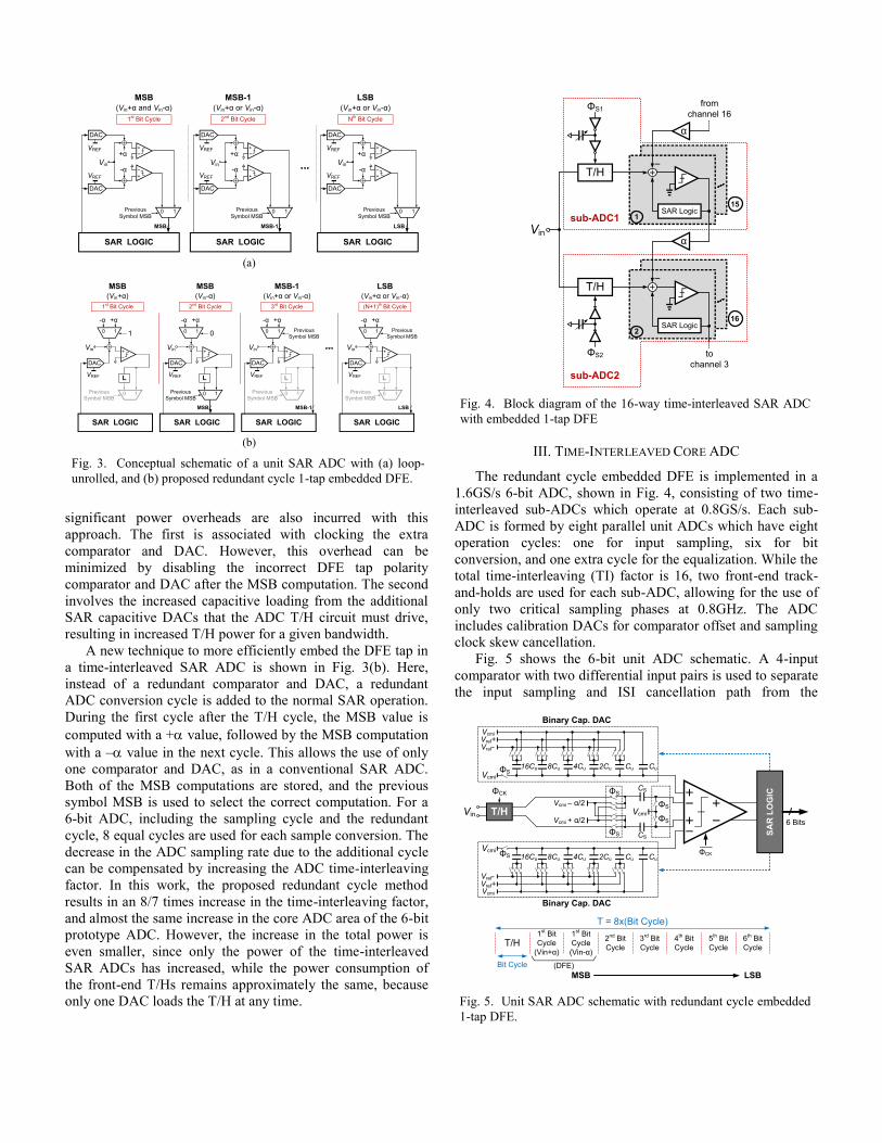
Fig. 3. Conceptual schematic of a unit SAR ADC with (a) loop-
unrolled, and (b) proposed redundant cycle 1-tap embedded DFE.
T/H
SAR Logic
α
SAR Logic
1
2
Vin
from
channel 16ΦS1
T/H
α
to
channel 3
16
15
ΦS2
sub-ADC1
sub-ADC2
Fig. 4. Block diagram of the 16-way time-interleaved SAR ADC
with embedded 1-tap DFE
Vin
ΦCK
SA
R L
OG
IC
6 Bits
CS
ΦS
ΦCK
T/H1
st Bit
Cycle
(Vin+α)
2nd
Bit
Cycle
3rd
Bit
Cycle
4th Bit
Cycle
5th Bit
Cycle
6th Bit
Cycle
T = 8x(Bit Cycle)
Bit Cycle
MSB LSB
Binary Cap. DAC
CuΦSVcmi
CS
Vref+Vref-
Vcmi + α/2
Vcmi
ΦS
ΦS
ΦS
Vcmi
1st Bit
Cycle
(Vin-α)
(DFE)
Vcmi – α/2
Cu2Cu4Cu8Cu16Cu
T/H
Binary Cap. DAC
CuΦS
Vcmi
Vref+Vref-
Vcmi
Cu2Cu4Cu8Cu16Cu
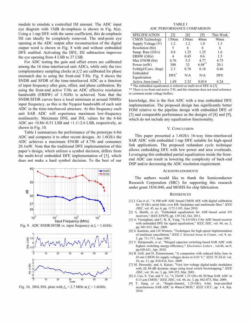
Fig. 5. Unit SAR ADC schematic with redundant cycle embedded
1-tap DFE.
significant power overheads are also incurred with this
approach. The first is associated with clocking the extra
comparator and DAC. However, this overhead can be
minimized by disabling the incorrect DFE tap polarity
comparator and DAC after the MSB computation. The second
involves the increased capacitive loading from the additional
SAR capacitive DACs that the ADC T/H circuit must drive,
resulting in increased T/H power for a given bandwidth.
A new technique to more efficiently embed the DFE tap in
a time-interleaved SAR ADC is shown in Fig. 3(b). Here,
instead of a redundant comparator and DAC, a redundant
ADC conversion cycle is added to the normal SAR operation.
During the first cycle after the T/H cycle, the MSB value is
computed with a + value, followed by the MSB computation
with a – value in the next cycle. This allows the use of only
one comparator and DAC, as in a conventional SAR ADC.
Both of the MSB computations are stored, and the previous
symbol MSB is used to select the correct computation. For a
6-bit ADC, including the sampling cycle and the redundant
cycle, 8 equal cycles are used for each sample conversion. The
decrease in the ADC sampling rate due to the additional cycle
can be compensated by increasing the ADC time-interleaving
factor. In this work, the proposed redundant cycle method
results in an 8/7 times increase in the time-interleaving factor,
and almost the same increase in the core ADC area of the 6-bit
prototype ADC. However, the increase in the total power is
even smaller, since only the power of the time-interleaved
SAR ADCs has increased, while the power consumption of
the front-end T/Hs remains approximately the same, because
only one DAC loads the T/H at any time.
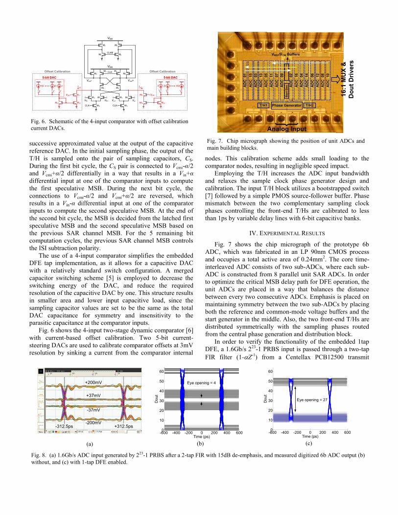
III. TIME-INTERLEAVED CORE ADC
The redundant cycle embedded DFE is implemented in a
1.6GS/s 6-bit ADC, shown in Fig. 4, consisting of two time-
interleaved sub-ADCs which operate at 0.8GS/s. Each sub-
ADC is formed by eight parallel unit ADCs which have eight
operation cycles: one for input sampling, six for bit
conversion, and one extra cycle for the equalization. While the
total time-interleaving (TI) factor is 16, two front-end track-
and-holds are used for each sub-ADC, allowing for the use of
only two critical sampling phases at 0.8GHz. The ADC
includes calibration DACs for comparator offset and sampling
clock skew cancellation.
Fig. 5 shows the 6-bit unit ADC schematic. A 4-input
comparator with two differential input pairs is used to separate
the input sampling and ISI cancellation path from the
VDD
Vin-Vin+
M3 M3
M2M2
CLK
Vout+Vout-
M4
CLK
M1rM1i
MTi
M4
VDD
M5M5
M6M6
CLKB
VDD MC1
MC2MC3
I2I16I
5-bit DAC
VDDMC1
MC2 MC3
I 2I 16I
5-bit DAC
VR+VR-
CLK
M1iM1r
MTr
Offset Calibration
Ical+
Offset Calibration
Ical-
Fig. 6. Schematic of the 4-input comparator with offset calibration
current DACs.
AD
C
01
AD
C
15
AD
C
03
AD
C
13
AD
C
05
AD
C
11
AD
C
07
AD
C
09
AD
C
02
AD
C
16
AD
C
04
AD
C
14
AD
C
06
AD
C
12
AD
C
08
AD
C
10
16
:1 M
UX
&
Do
ut
Dri
ve
rs
Phase GeneratorT/H1 T/H2
Analog Input
Sta
rt G
en
.
VREF/VCM Buffers
Fig. 7. Chip micrograph showing the position of unit ADCs and
main building blocks.
+200mV
+37mV
-37mV
-200mV-312.5ps +312.5ps
(a)
-600 -400 -200 0 200 400 6000
10
20
30
40
50
60
Time (ps)
Do
ut
Eye opening = 4
(b)
-600 -400 -200 0 200 400 6000
10
20
30
40
50
60
Time (ps)
Do
ut
Eye opening = 27
(c)
Fig. 8. (a) 1.6Gb/s ADC input generated by 223-1 PRBS after a 2-tap FIR with 15dB de-emphasis, and measured digitized 6b ADC output (b)
without, and (c) with 1-tap DFE enabled.
successive approximated value at the output of the capacitive
reference DAC. In the initial sampling phase, the output of the
T/H is sampled onto the pair of sampling capacitors, CS.
During the first bit cycle, the CS pair is connected to Vcmi-α/2
and Vcmi+α/2 differentially in a way that results in a Vin+α
differential input at one of the comparator inputs to compute
the first speculative MSB. During the next bit cycle, the
connections to Vcmi-α/2 and Vcmi+α/2 are reversed, which
results in a Vin-α differential input at one of the comparator
inputs to compute the second speculative MSB. At the end of
the second bit cycle, the MSB is decided from the latched first
speculative MSB and the second speculative MSB based on
the previous SAR channel MSB. For the 5 remaining bit
computation cycles, the previous SAR channel MSB controls
the ISI subtraction polarity.
The use of a 4-input comparator simplifies the embedded
DFE tap implementation, as it allows for a capacitive DAC
with a relatively standard switch configuration. A merged
capacitor switching scheme [5] is employed to decrease the
switching energy of the DAC, and reduce the required
resolution of the capacitive DAC by one. This structure results
in smaller area and lower input capacitive load, since the
sampling capacitor values are set to be the same as the total
DAC capacitance for symmetry and insensitivity to the
parasitic capacitance at the comparator inputs.
Fig. 6 shows the 4-input two-stage dynamic comparator [6]
with current-based offset calibration. Two 5-bit current-
steering DACs are used to calibrate comparator offsets at 3mV
resolution by sinking a current from the comparator internal
nodes. This calibration scheme adds small loading to the
comparator nodes, resulting in negligible speed impact.
Employing the T/H increases the ADC input bandwidth
and relaxes the sample clock phase generator design and
calibration. The input T/H block utilizes a bootstrapped switch
[7] followed by a simple PMOS source-follower buffer. Phase
mismatch between the two complementary sampling clock
phases controlling the front-end T/Hs are calibrated to less
than 1ps by variable delay lines with 6-bit capacitive banks.
IV. EXPERIMENTAL RESULTS
Fig. 7 shows the chip micrograph of the prototype 6b
ADC, which was fabricated in an LP 90nm CMOS process
and occupies a total active area of 0.24mm2. The core time-
interleaved ADC consists of two sub-ADCs, where each sub-
ADC is constructed from 8 parallel unit SAR ADCs. In order
to optimize the critical MSB delay path for DFE operation, the
unit ADCs are placed in a way that balances the distance
between every two consecutive ADCs. Emphasis is placed on
maintaining symmetry between the two sub-ADCs by placing
both the reference and common-mode voltage buffers and the
start generator in the middle. Also, the two front-end T/Hs are
distributed symmetrically with the sampling phases routed
from the central phase generation and distribution block.
In order to verify the functionality of the embedded 1tap
DFE, a 1.6Gb/s 223
-1 PRBS input is passed through a two-tap
FIR filter (1-Z-1
) from a Centellax PCB12500 transmit
module to emulate a controlled ISI amount. The ADC input
eye diagram with 15dB de-emphasis is shown in Fig. 8(a).
Using a 1-tap DFE with the same coefficient, this de-emphasis
ISI can ideally be completely removed. The mid-point eye
opening at the ADC output after reconstruction of the digital
output word is shown in Fig. 8 with and without embedded
DFE enabled. Activating the DFE, ISI subtraction improves
the eye opening from 4 LSB to 27 LSB.
For ADC testing the gain and offset errors are calibrated
among the 16 time-interleaved unit ADCs, while only the two
complementary sampling clocks at fs/2 are calibrated for phase
mismatch due to using the front-end T/Hs. Fig. 9 shows the
SNDR and SFDR of the time-interleaved ADC as a function
of input frequency after gain, offset, and phase calibration. By
using the front-end active T/Hs an ADC effective resolution
bandwidth (ERBW) of 1.5GHz is achieved. Note that the
SNDR/SFDR curves have a local minimum at around 50MHz
input frequency, as this is the Nyquist bandwidth of each unit
ADC in the time-interleaved structure. At this frequency each
unit SAR ADC will experience maximum low-frequency
nonlinearity. Maximum DNL and INL values for the 6-bit
ADC are +0.68/-0.51 LSB and +1.1/-2.8 LSB, respectively, as
shown in Fig. 10.
Table I summarizes the performance of the prototype 6-bit
ADC and compares it to other recent designs. At 1.6GS/s the
ADC achieves a maximum ENOB of 4.75b and consumes
20.1mW. Note that the traditional DFE implementation of this
paper’s design, which utilizes a symbol decision, differs from
the multi-level embedded DFE implementation of [3], which
does not make a hard symbol decision. To the best of our
knowledge, this is the first ADC with a true embedded DFE
implementation. The proposed design has significantly better
FOM relative to the pipeline design with embedded DFE of
[3] and comparable performance as the designs of [8] and [9],
which do not include any equalization functionality.
V. CONCLUSION
This paper presented a 1.6GS/s 16-way time-interleaved
SAR ADC with embedded 1-tap DFE suitable for high-speed
link applications. The proposed redundant cycle technique
allows embedding DFE with low power and area overheads.
Leveraging this embedded partial equalization inside the front-
end ADC can result in lowering the complexity of back-end
DSP and/or decreasing the ADC resolution requirement.
ACKNOWLEDGMENTS
The authors would like to thank the Semiconductor
Research Corporation (SRC) for supporting this research
under grant 1836.040, and MOSIS for chip fabrication.
REFERENCES
[1] J. Cao et al., "A 500 mW ADC-based CMOS AFE with digital calibration
for 10 Gb/s serial links over KR- backplane and multimode fiber," IEEE JSSC, vol. 45, no. 6, pp. 1172-1185, June 2010.
[2] A. Shafik, et al., "Embedded equalization for ADC-based serial I/O
receivers," IEEE EPEPS, pp. 139-142, Oct. 2011. [3] A. Varzaghani, and C.-K. K. Yang, "A 4.8 GS/s 5-bit ADC-based receiver
with embedded DFE for signal equalization," IEEE JSSC, vol. 44, no. 3,
pp. 901-915, Mar. 2009. [4] S. Kasturia, and J.H Winters, "Techniques for high-speed implementation
of nonlinear cancellation," IEEE J. Selected Areas in Comm., vol. 9, no.
5, pp. 711-717, June 1991. [5] V. Hariprasath, et al., "Merged capacitor switching based SAR ADC with
highest switching energy-efficiency," Electronics Letters , vol.46, no.9,
pp.620-621, Apr. 2010. [6] B. Goll, and H. Zimmermann, "A comparator with reduced delay time in
65-nm CMOS for supply voltages down to 0.65 V," IEEE TCAS-II, vol.
56, no. 11, pp. 810-814, Nov. 2009. [7] M. Dessouky, and A. Kaiser, "Very low-voltage digital-audio modulator
with ΔΣ 88-dB dynamic range using local switch bootstrapping," IEEE
JSSC, vol. 36, no. 3, pp. 349-355, Mar. 2001. [8] Z. Cao, S. Yan, and Y. Li, "A 32mW 1.25 GS/s 6b 2b/Step SAR ADC in
0.13 µm CMOS," IEEE JSSC, vol. 44, no. 3, pp. 862-873, Mar. 2009.
[9] T. Jiang, et al., "Single-channel, 1.25-GS/s, 6-bit, loop-unrolled asynchronous SAR-ADC in 40nm-CMOS," IEEE CICC, pp. 1-4, Sep.
2010.
100
101
102
103
25
27
30
35
40
Input Frequency (MHz)
dB
SNDR
SFDR
Fig. 9. ADC SNDR/SFDR vs. input frequency at fs = 1.6GHz.
0 10 20 30 40 50 60-1
-0.5
0
0.5
1
DN
L (
LS
B)
0 10 20 30 40 50 60-3
-2
-1
0
1
2
3
Code
INL (
LS
B)
Fig. 10. DNL/INL plots with fin = 2.7 MHz at fs = 1.6GHz.
TABLE I
ADC PERFORMANCE COMPARISON
SPECIFICATION [3] [8] [9] This Work
CMOS Technology 130nm 130nm 40nm 90nm
Supply Voltage (V) 1.2 1.2 1.0 1.3
Resolution (bit) 5 6 6 6
Samp. Rate (GS/s) 4.8 1.25 1.25 1.6
ERBW (GHz) 4 0.45 0.6 1.5
Max ENOB (bit) 4.76 5.5 4.77 4.75
Power (mW) 300 32 6.08** 20.1
FoM(pJ/Conv.-Step) 2.3 0.78 0.18 0.46
Embedded
Equalization DFE* N/A N/A DFE
Active Area (mm2) 1.69 2.32 0.014 0.24 * The embedded equalization is referred as multi-level DFE in [3].
** There is no front-end active T/H, and this structure does not need reference
or common-mode voltage buffers.


![CommunicationofMultipleBits: [Ch.14]schniter/ee702/handouts/m_ary.pdf · 2012-03-25 · PhilSchniter OSUECE-702 CommunicationofMultipleBits: [Ch.14] Problem Setup: • Kb bits ⇒](https://static.fdocument.org/doc/165x107/5ed78070e200687e44403fb1/communicationofmultiplebits-ch14-schniteree702handoutsmarypdf-2012-03-25.jpg)