LTC2270 - 16-Bit, 20Msps Low Noise Dual ADC - Linear...
36
1 2270f LTC2270 TYPICAL APPLICATION FEATURES APPLICATIONS DESCRIPTION 16-Bit, 20Msps Low Noise Dual ADC n Low Power Instrumentation n Software Defined Radios n Portable Medical Imaging n Multi-Channel Data Acquisition n Two-Channel Simultaneously Sampling ADC n 84.1dB SNR (46μV RMS Input Referred Noise) n 99dB SFDR n ±2.3LSB INL(Max) n Low Power: 160mW Total, 80mW per Channel n Single 1.8V Supply n CMOS, DDR CMOS, or DDR LVDS Outputs n Selectable Input Ranges: 1V P-P to 2.1V P-P n 200MHz Full Power Bandwidth S/H n Shutdown and Nap Modes n Serial SPI Port for Configuration n Pin Compatible with LTC2180: 16-Bit, 25Msps, 78mW LTC2140-14: 14-Bit, 25Msps, 50mW n 64-Lead (9mm × 9mm) QFN Package The LTC ® 2270 is a two-channel simultaneous sampling 16-bit A/D converter designed for digitizing high frequency, wide dynamic range signals. It is perfect for demanding applications with AC performance that includes 84.1dB SNR and 99dB spurious free dynamic range (SFDR). DC specs include ±1LSB INL (typ), ±0.2LSB DNL (typ) and no missing codes over temperature. The transition noise is 1.44LSB RMS . The digital outputs can be either full rate CMOS, Double Data Rate CMOS, or Double Data Rate LVDS. A separate output power supply allows the CMOS output swing to range from 1.2V to 1.8V. The ENC + and ENC – inputs may be driven differentially or single-ended with a sine wave, PECL, LVDS, TTL, or CMOS inputs. An optional clock duty cycle stabilizer al- lows high performance at full speed for a wide range of clock duty cycles. L, LT, LTC, LTM, Linear Technology and the Linear logo are registered trademarks of Linear Technology Corporation. All other trademarks are the property of their respective owners. Integral Non-Linearity (INL) CMOS, DDR CMOS OR DDR LVDS OUTPUTS 1.8V V DD 1.8V OV DD CLOCK CONTROL D1_15 D1_0 2270 TA01 CH 1 ANALOG INPUT OUTPUT DRIVERS GND OGND S/H 16-BIT ADC CORE CH 2 ANALOG INPUT S/H 16-BIT ADC CORE D2_15 D2_0 20MHz CLOCK OUTPUT CODE 0 –2.0 –1.5 –1.0 INL ERROR (LSB) –0.5 0.5 0.0 1.0 1.5 2.0 16384 32768 49152 65536 2270 TA02
Transcript of LTC2270 - 16-Bit, 20Msps Low Noise Dual ADC - Linear...
12270f
LTC2270
TYPICAL APPLICATION
FEATURES
APPLICATIONS
DESCRIPTION
16-Bit, 20Msps Low Noise Dual ADC
n Low Power Instrumentationn Software Defined Radiosn Portable Medical Imagingn Multi-Channel Data Acquisition
n Two-Channel Simultaneously Sampling ADCn 84.1dB SNR (46μVRMS Input Referred Noise)n 99dB SFDRn ±2.3LSB INL(Max)n Low Power: 160mW Total, 80mW per Channeln Single 1.8V Supplyn CMOS, DDR CMOS, or DDR LVDS Outputsn Selectable Input Ranges: 1VP-P to 2.1VP-Pn 200MHz Full Power Bandwidth S/Hn Shutdown and Nap Modesn Serial SPI Port for Configurationn Pin Compatible with LTC2180: 16-Bit, 25Msps, 78mW LTC2140-14: 14-Bit, 25Msps, 50mWn 64-Lead (9mm × 9mm) QFN Package
The LTC®2270 is a two-channel simultaneous sampling 16-bit A/D converter designed for digitizing high frequency, wide dynamic range signals. It is perfect for demanding applications with AC performance that includes 84.1dB SNR and 99dB spurious free dynamic range (SFDR).
DC specs include ±1LSB INL (typ), ±0.2LSB DNL (typ) and no missing codes over temperature. The transition noise is 1.44LSBRMS.
The digital outputs can be either full rate CMOS, Double Data Rate CMOS, or Double Data Rate LVDS. A separate output power supply allows the CMOS output swing to range from 1.2V to 1.8V.
The ENC+ and ENC– inputs may be driven differentially or single-ended with a sine wave, PECL, LVDS, TTL, or CMOS inputs. An optional clock duty cycle stabilizer al-lows high performance at full speed for a wide range of clock duty cycles.L, LT, LTC, LTM, Linear Technology and the Linear logo are registered trademarks of Linear Technology Corporation. All other trademarks are the property of their respective owners.
Integral Non-Linearity (INL)
CMOS,DDR CMOSOR DDR LVDSOUTPUTS
1.8V
VDD
1.8V
OVDD
CLOCKCONTROL
D1_15
D1_0
2270 TA01
CH 1ANALOG
INPUT
OUTPUTDRIVERS
GND OGND
S/H16-BIT
ADC CORE
CH 2ANALOG
INPUTS/H
16-BITADC CORE
D2_15
D2_0
20MHzCLOCK OUTPUT CODE
0–2.0
–1.5
–1.0
INL
ERRO
R (L
SB)
–0.5
0.5
0.0
1.0
1.5
2.0
16384 32768 49152 65536
2270 TA02
LTC2270
22270f
ABSOLUTE MAXIMUM RATINGSSupply Voltages (VDD, OVDD) ....................... –0.3V to 2VAnalog Input Voltage (AIN
+, AIN–,
PAR/SER, SENSE) (Note 3) .......... –0.3V to (VDD + 0.2V)Digital Input Voltage (ENC+, ENC–, CS, SDI, SCK) (Note 4) .................................... –0.3V to 3.9VSDO (Note 4) ............................................. –0.3V to 3.9V
(Notes 1, 2)
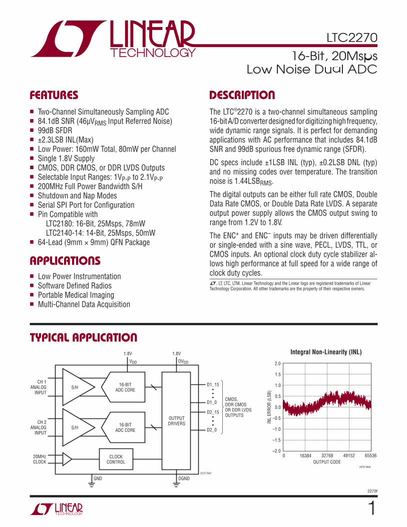
PIN CONFIGURATIONS
Digital Output Voltage ................ –0.3V to (OVDD + 0.3V)Operating Temperature Range
LTC2270C ................................................ 0°C to 70°CLTC2270I .............................................–40°C to 85°C
Storage Temperature Range .................. –65°C to 150°C
FULL-RATE CMOS OUTPUT MODE DOUBLE DATA RATE CMOS OUTPUT MODE
TOP VIEW
UP PACKAGE64-LEAD (9mm 9mm) PLASTIC QFN
VDD 1
VCM1 2
GND 3
AIN1+ 4
AIN1– 5
GND 6
REFH 7
REFL 8
REFH 9
REFL 10
PAR/SER 11
AIN2+ 12
AIN2– 13
GND 14
VCM2 15
VDD 16
48 D1_5
47 D1_4
46 D1_3
45 D1_2
44 D1_1
43 D1_0
42 OVDD
41 OGND
40 CLKOUT+
39 CLKOUT–
38 D2_15
37 D2_14
36 D2_13
35 D2_12
34 D2_11
33 D2_10
65GND
64 V
DD
63 S
EN
SE
62 V
REF
61 S
DO
60 O
F1
59 O
F2
58 D
1_15
57 D
1_14
56 D
1_13
55 D
1_12
54 D
1_11
53 D
1_10
52 D
1_9
51 D
1_8
50 D
1_7
49 D
1_6
VD
D 1
7
EN
C+ 1
8
EN
C– 1
9
CS
20
SC
K 2
1
SD
I 22
D2_0 2
3
D2_1 2
4
D2_2 2
5
D2_3 2
6
D2_4 2
7
D2_5 2
8
D2_6 2
9
D2_7 3
0
D2_8 3
1
D2_9 3
2
TJMAX = 150°C, θJA = 20°C/WEXPOSED PAD (PIN 65) IS GND, MUST BE SOLDERED TO PCB
TOP VIEW
UP PACKAGE64-LEAD (9mm 9mm) PLASTIC QFN
VDD 1
VCM1 2
GND 3
AIN1+ 4
AIN1– 5
GND 6
REFH 7
REFL 8
REFH 9
REFL 10
PAR/SER 11
AIN2+ 12
AIN2– 13
GND 14
VCM2 15
VDD 16
48 D1_4_5
47 DNC
46 D1_2_3
45 DNC
44 D1_0_1
43 DNC
42 OVDD
41 OGND
40 CLKOUT+
39 CLKOUT–
38 D2_14_15
37 DNC
36 D2_12_13
35 DNC
34 D2_10_11
33 DNC
65GND
64 V
DD
63 S
EN
SE
62 V
REF
61 S
DO
60 O
F2_1
59 D
NC
58 D
1_14_15
57 D
NC
56 D
1_12_13
55 D
NC
54 D
1_10_11
53 D
NC
52 D
1_8_9
51 D
NC
50 D
1_6_7
49 D
NC
VD
D 1
7
EN
C+ 1
8
EN
C– 1
9
CS
20
SC
K 2
1
SD
I 22
DN
C 2
3
D2_0_1 2
4
DN
C 2
5
D2_2_3 2
6
DN
C 2
7
D2_4_5 2
8
DN
C 2
9
D2_6_7 3
0
DN
C 3
1
D2_8_9 3
2
TJMAX = 150°C, θJA = 20°C/WEXPOSED PAD (PIN 65) IS GND, MUST BE SOLDERED TO PCB
32270f
LTC2270
ORDER INFORMATIONLEAD FREE FINISH TAPE AND REEL PART MARKING* PACKAGE DESCRIPTION TEMPERATURE RANGE
LTC2270CUP#PBF LTC2270CUP#TRPBF LTC2270UP 64-Lead (9mm × 9mm) Plastic QFN 0°C to 70°C
LTC2270IUP#PBF LTC2270IUP#TRPBF LTC2270UP 64-Lead (9mm × 9mm) Plastic QFN –40°C to 85°C
Consult LTC Marketing for parts specified with wider operating temperature ranges. *The temperature grade is identified by a label on the shipping container.
Consult LTC Marketing for information on non-standard lead based finish parts.
For more information on lead free part marking, go to: http://www.linear.com/leadfree/ For more information on tape and reel specifications, go to: http://www.linear.com/tapeandreel/
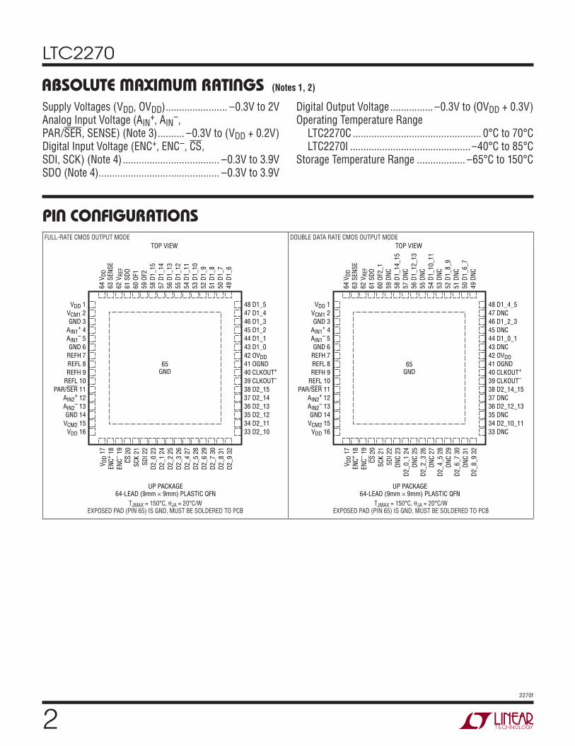
DOUBLE DATA RATE LVDS OUTPUT MODE
TOP VIEW
UP PACKAGE64-LEAD (9mm 9mm) PLASTIC QFN
VDD 1
VCM1 2
GND 3
AIN1+ 4
AIN1– 5
GND 6
REFH 7
REFL 8
REFH 9
REFL 10
PAR/SER 11
AIN2+ 12
AIN2– 13
GND 14
VCM2 15
VDD 16
48 D1_4_5+
47 D1_4_5–
46 D1_2_3+
45 D1_2_3–
44 D1_0_1+
43 D1_0_1–
42 OVDD
41 OGND
40 CLKOUT+
39 CLKOUT–
38 D2_14_15+
37 D2_14_15–
36 D2_12_13+
35 D2_12_13–
34 D2_10_11+
33 D2_10_11–
65GND
64 V
DD
63 S
EN
SE
62 V
REF
61 S
DO
60 O
F2_1
+
59 O
F2_1
–
58 D
1_14_15
+
57 D
1_14_15
–
56 D
1_12_13
+
55 D
1_12_13
–
54 D
1_10_11
+
53 D
1_10_11
–
52 D
1_8_9
+
51 D
1_8_9
–
50 D
1_6_7
+
49 D
1_6_7
–
VD
D 1
7
EN
C+ 1
8
EN
C– 1
9
CS
20
SC
K 2
1
SD
I 22
D2_0_1
– 2
3
D2_0_1
+ 2
4
D2_2_3
– 2
5
D2_2_3
+ 2
6
D2_4_5
– 2
7
D2_4_5
+ 2
8
D2_6_7
– 2
9
D2_6_7
+ 3
0
D2_8_9
– 3
1
D2_8_9
+ 3
2
TJMAX = 150°C, θJA = 20°C/WEXPOSED PAD (PIN 65) IS GND, MUST BE SOLDERED TO PCB
PIN CONFIGURATIONS
LTC2270
42270f
ANALOG INPUT The l denotes the specifications which apply over the full operating temperature range, otherwise specifications are at TA = 25°C. (Note 5)
SYMBOL PARAMETER CONDITIONS MIN TYP MAX UNITS
VIN Analog Input Range (AIN+ – AIN
–) 1.7V < VDD < 1.9V l 1 to 2.1 VP-P
VIN(CM) Analog Input Common Mode (AIN+ + AIN
–)/2 Differential Analog Input (Note 8) l 0.65 VCM VCM + 200mV V
VSENSE External Voltage Reference Applied to SENSE External Reference Mode l 0.625 1.250 1.300 V
IINCM Analog Input Common Mode Current Per Pin, 20Msps 32 μA
IIN1 Analog Input Leakage Current (No Encode) 0 < AIN+, AIN
– < VDD l –1 1 μA
IIN2 PAR/SER Input Leakage Current 0 < PAR/SER < VDD l –1 1 μA
IIN3 SENSE Input Leakage Current 0.625 < SENSE < 1.3V l –2 2 μA
tAP Sample-and-Hold Acquisition Delay Time 0 ns
tJITTER Sample-and-Hold Acquisition Delay Jitter Single-Ended EncodeDifferential Encode
85100
fsRMSfsRMS
CMRR Analog Input Common Mode Rejection Ratio 80 dB
BW-3B Full-Power Bandwidth Figure 5 Test Circuit 200 MHz
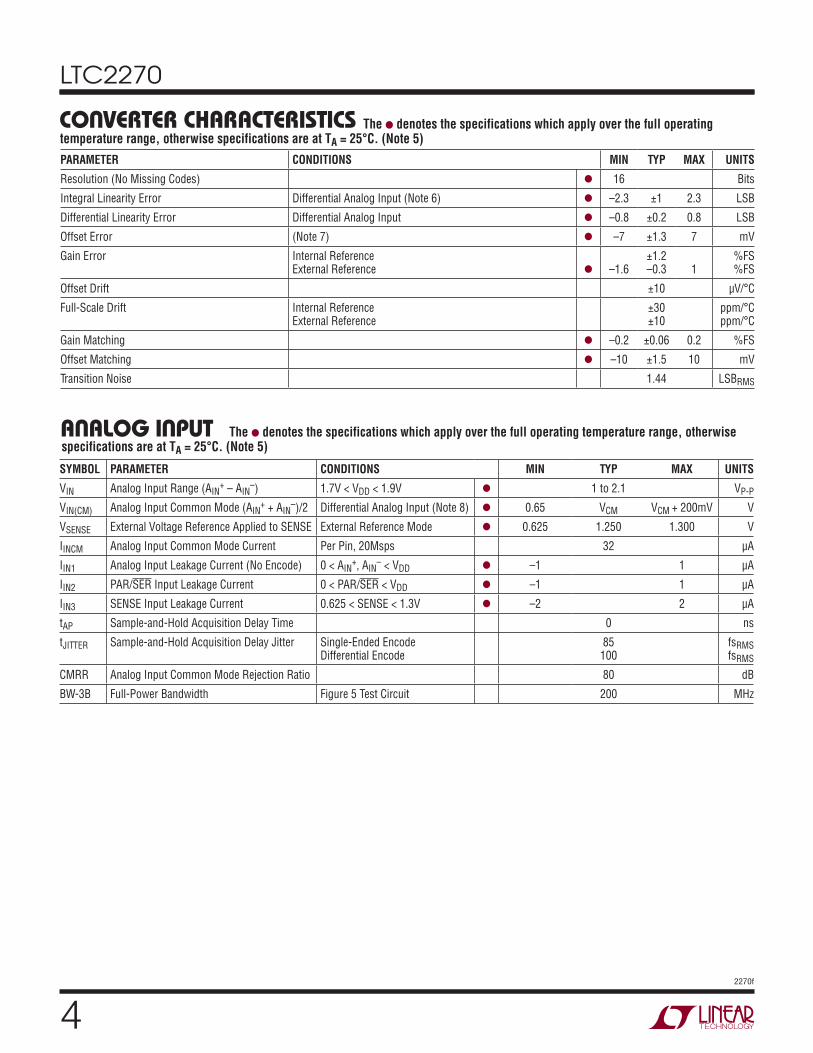
CONVERTER CHARACTERISTICS The l denotes the specifications which apply over the full operating temperature range, otherwise specifications are at TA = 25°C. (Note 5)
PARAMETER CONDITIONS MIN TYP MAX UNITS
Resolution (No Missing Codes) l 16 Bits
Integral Linearity Error Differential Analog Input (Note 6) l –2.3 ±1 2.3 LSB
Differential Linearity Error Differential Analog Input l –0.8 ±0.2 0.8 LSB
Offset Error (Note 7) l –7 ±1.3 7 mV
Gain Error Internal ReferenceExternal Reference l –1.6
±1.2–0.3 1
%FS%FS
Offset Drift ±10 μV/°C
Full-Scale Drift Internal ReferenceExternal Reference
±30±10
ppm/°Cppm/°C
Gain Matching l –0.2 ±0.06 0.2 %FS
Offset Matching l –10 ±1.5 10 mV
Transition Noise 1.44 LSBRMS
52270f
LTC2270
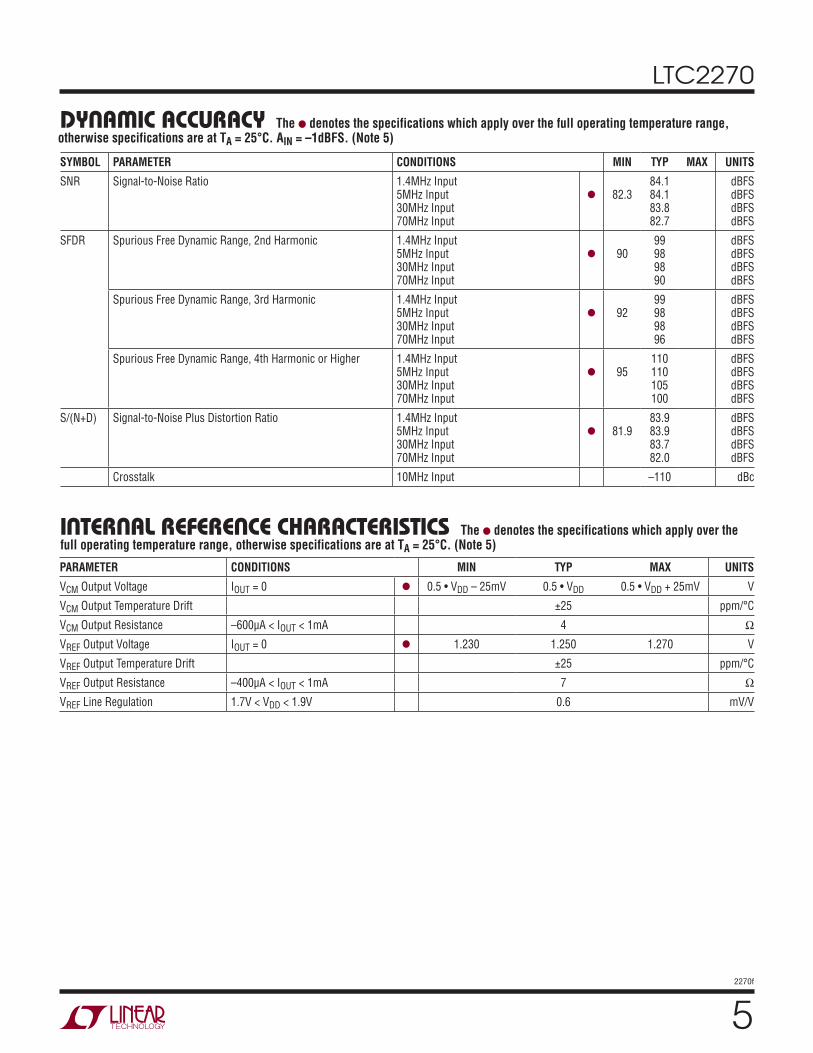
INTERNAL REFERENCE CHARACTERISTICS The l denotes the specifications which apply over the full operating temperature range, otherwise specifications are at TA = 25°C. (Note 5)
PARAMETER CONDITIONS MIN TYP MAX UNITS
VCM Output Voltage IOUT = 0 l 0.5 • VDD – 25mV 0.5 • VDD 0.5 • VDD + 25mV V
VCM Output Temperature Drift ±25 ppm/°C
VCM Output Resistance –600μA < IOUT < 1mA 4 Ω
VREF Output Voltage IOUT = 0 l 1.230 1.250 1.270 V
VREF Output Temperature Drift ±25 ppm/°C
VREF Output Resistance –400μA < IOUT < 1mA 7 Ω
VREF Line Regulation 1.7V < VDD < 1.9V 0.6 mV/V
DYNAMIC ACCURACY The l denotes the specifications which apply over the full operating temperature range, otherwise specifications are at TA = 25°C. AIN = –1dBFS. (Note 5)
SYMBOL PARAMETER CONDITIONS MIN TYP MAX UNITS
SNR Signal-to-Noise Ratio 1.4MHz Input5MHz Input30MHz Input70MHz Input
l 82.384.184.183.882.7
dBFSdBFSdBFSdBFS
SFDR Spurious Free Dynamic Range, 2nd Harmonic 1.4MHz Input5MHz Input30MHz Input70MHz Input
l 9099989890
dBFSdBFSdBFSdBFS
Spurious Free Dynamic Range, 3rd Harmonic 1.4MHz Input5MHz Input30MHz Input70MHz Input
l 9299989896
dBFSdBFSdBFSdBFS
Spurious Free Dynamic Range, 4th Harmonic or Higher 1.4MHz Input5MHz Input30MHz Input70MHz Input
l 95110110105100
dBFSdBFSdBFSdBFS
S/(N+D) Signal-to-Noise Plus Distortion Ratio 1.4MHz Input5MHz Input30MHz Input70MHz Input
l 81.983.983.983.782.0
dBFSdBFSdBFSdBFS
Crosstalk 10MHz Input –110 dBc
LTC2270
62270f
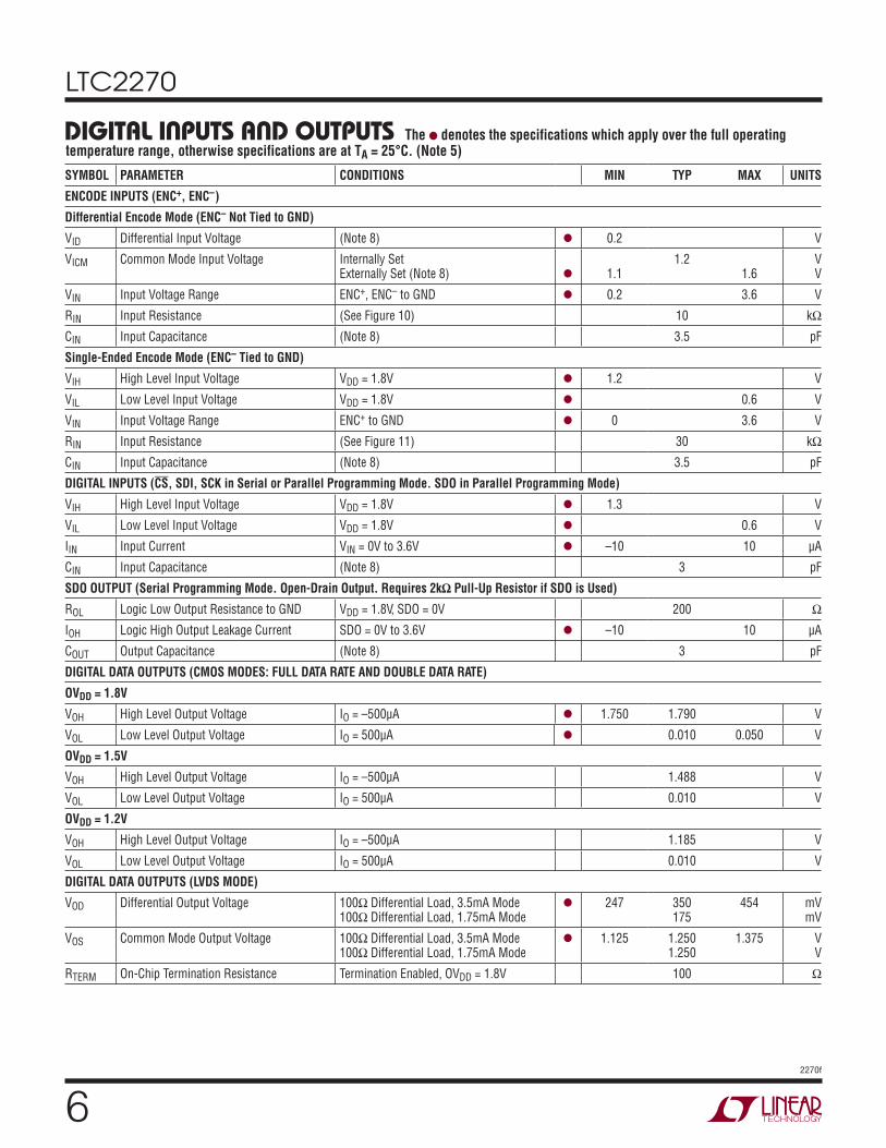
DIGITAL INPUTS AND OUTPUTS The l denotes the specifications which apply over the full operating temperature range, otherwise specifications are at TA = 25°C. (Note 5)
SYMBOL PARAMETER CONDITIONS MIN TYP MAX UNITS
ENCODE INPUTS (ENC+, ENC– )
Differential Encode Mode (ENC– Not Tied to GND)
VID Differential Input Voltage (Note 8) l 0.2 V
VICM Common Mode Input Voltage Internally SetExternally Set (Note 8) l 1.1
1.21.6
VV
VIN Input Voltage Range ENC+, ENC– to GND l 0.2 3.6 V
RIN Input Resistance (See Figure 10) 10 kΩ
CIN Input Capacitance (Note 8) 3.5 pF
Single-Ended Encode Mode (ENC– Tied to GND)
VIH High Level Input Voltage VDD = 1.8V l 1.2 V
VIL Low Level Input Voltage VDD = 1.8V l 0.6 V
VIN Input Voltage Range ENC+ to GND l 0 3.6 V
RIN Input Resistance (See Figure 11) 30 kΩ
CIN Input Capacitance (Note 8) 3.5 pF
DIGITAL INPUTS (CS, SDI, SCK in Serial or Parallel Programming Mode. SDO in Parallel Programming Mode)
VIH High Level Input Voltage VDD = 1.8V l 1.3 V
VIL Low Level Input Voltage VDD = 1.8V l 0.6 V
IIN Input Current VIN = 0V to 3.6V l –10 10 μA
CIN Input Capacitance (Note 8) 3 pF
SDO OUTPUT (Serial Programming Mode. Open-Drain Output. Requires 2kΩ Pull-Up Resistor if SDO is Used)
ROL Logic Low Output Resistance to GND VDD = 1.8V, SDO = 0V 200 Ω
IOH Logic High Output Leakage Current SDO = 0V to 3.6V l –10 10 μA
COUT Output Capacitance (Note 8) 3 pF
DIGITAL DATA OUTPUTS (CMOS MODES: FULL DATA RATE AND DOUBLE DATA RATE)
OVDD = 1.8V
VOH High Level Output Voltage IO = –500μA l 1.750 1.790 V
VOL Low Level Output Voltage IO = 500μA l 0.010 0.050 V
OVDD = 1.5V
VOH High Level Output Voltage IO = –500μA 1.488 V
VOL Low Level Output Voltage IO = 500μA 0.010 V
OVDD = 1.2V
VOH High Level Output Voltage IO = –500μA 1.185 V
VOL Low Level Output Voltage IO = 500μA 0.010 V
DIGITAL DATA OUTPUTS (LVDS MODE)
VOD Differential Output Voltage 100Ω Differential Load, 3.5mA Mode100Ω Differential Load, 1.75mA Mode
l 247 350175
454 mVmV
VOS Common Mode Output Voltage 100Ω Differential Load, 3.5mA Mode100Ω Differential Load, 1.75mA Mode
l 1.125 1.2501.250
1.375 VV
RTERM On-Chip Termination Resistance Termination Enabled, OVDD = 1.8V 100 Ω
72270f
LTC2270
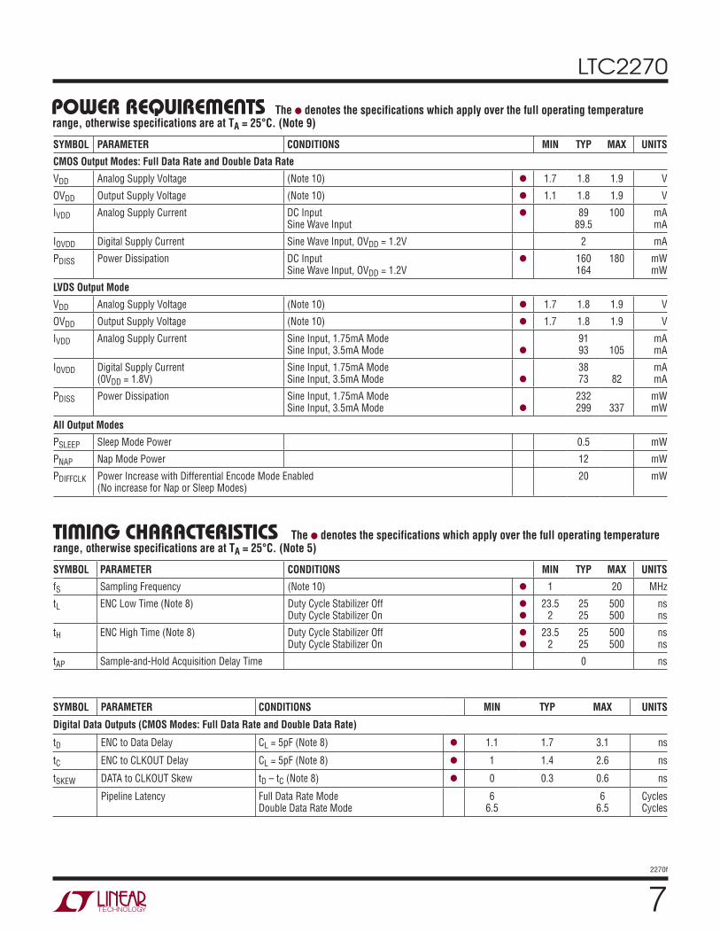
POWER REQUIREMENTS The l denotes the specifications which apply over the full operating temperature range, otherwise specifications are at TA = 25°C. (Note 9)
SYMBOL PARAMETER CONDITIONS MIN TYP MAX UNITS
CMOS Output Modes: Full Data Rate and Double Data Rate
VDD Analog Supply Voltage (Note 10) l 1.7 1.8 1.9 V
OVDD Output Supply Voltage (Note 10) l 1.1 1.8 1.9 V
IVDD Analog Supply Current DC InputSine Wave Input
l 8989.5
100 mAmA
IOVDD Digital Supply Current Sine Wave Input, OVDD = 1.2V 2 mA
PDISS Power Dissipation DC InputSine Wave Input, OVDD = 1.2V
l 160164
180 mWmW
LVDS Output Mode
VDD Analog Supply Voltage (Note 10) l 1.7 1.8 1.9 V
OVDD Output Supply Voltage (Note 10) l 1.7 1.8 1.9 V
IVDD Analog Supply Current Sine Input, 1.75mA ModeSine Input, 3.5mA Mode l
9193 105
mAmA
IOVDD Digital Supply Current(0VDD = 1.8V)
Sine Input, 1.75mA ModeSine Input, 3.5mA Mode l
3873 82
mAmA
PDISS Power Dissipation Sine Input, 1.75mA ModeSine Input, 3.5mA Mode l
232299 337
mWmW
All Output Modes
PSLEEP Sleep Mode Power 0.5 mW
PNAP Nap Mode Power 12 mW
PDIFFCLK Power Increase with Differential Encode Mode Enabled(No increase for Nap or Sleep Modes)
20 mW
TIMING CHARACTERISTICS The l denotes the specifications which apply over the full operating temperature range, otherwise specifications are at TA = 25°C. (Note 5)
SYMBOL PARAMETER CONDITIONS MIN TYP MAX UNITS
fS Sampling Frequency (Note 10) l 1 20 MHz
tL ENC Low Time (Note 8) Duty Cycle Stabilizer OffDuty Cycle Stabilizer On
l
l
23.52
2525
500500
nsns
tH ENC High Time (Note 8) Duty Cycle Stabilizer OffDuty Cycle Stabilizer On
l
l
23.52
2525
500500
nsns
tAP Sample-and-Hold Acquisition Delay Time 0 ns
SYMBOL PARAMETER CONDITIONS MIN TYP MAX UNITS
Digital Data Outputs (CMOS Modes: Full Data Rate and Double Data Rate)
tD ENC to Data Delay CL = 5pF (Note 8) l 1.1 1.7 3.1 ns
tC ENC to CLKOUT Delay CL = 5pF (Note 8) l 1 1.4 2.6 ns
tSKEW DATA to CLKOUT Skew tD – tC (Note 8) l 0 0.3 0.6 ns
Pipeline Latency Full Data Rate ModeDouble Data Rate Mode
66.5
66.5
CyclesCycles
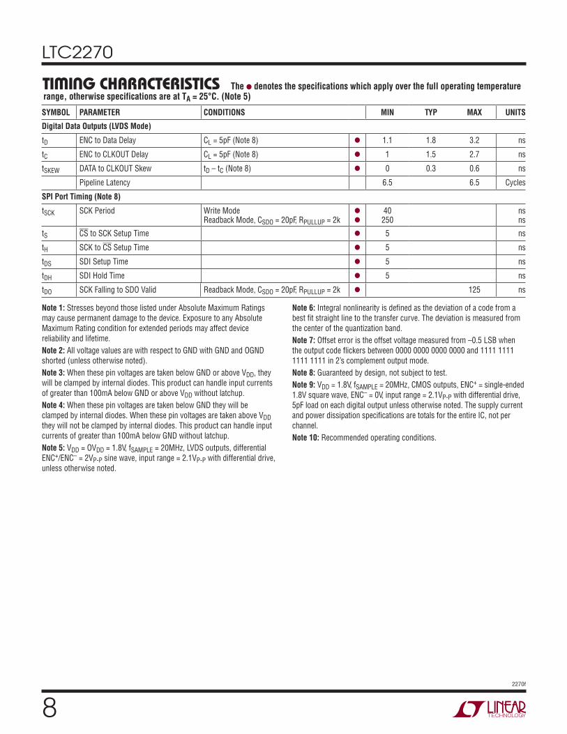
LTC2270
82270f
SYMBOL PARAMETER CONDITIONS MIN TYP MAX UNITS
Digital Data Outputs (LVDS Mode)
tD ENC to Data Delay CL = 5pF (Note 8) l 1.1 1.8 3.2 ns
tC ENC to CLKOUT Delay CL = 5pF (Note 8) l 1 1.5 2.7 ns
tSKEW DATA to CLKOUT Skew tD – tC (Note 8) l 0 0.3 0.6 ns
Pipeline Latency 6.5 6.5 Cycles
SPI Port Timing (Note 8)
tSCK SCK Period Write ModeReadback Mode, CSDO = 20pF, RPULLUP = 2k
l
l
40250
nsns
tS CS to SCK Setup Time l 5 ns
tH SCK to CS Setup Time l 5 ns
tDS SDI Setup Time l 5 ns
tDH SDI Hold Time l 5 ns
tDO SCK Falling to SDO Valid Readback Mode, CSDO = 20pF, RPULLUP = 2k l 125 ns
TIMING CHARACTERISTICS The l denotes the specifications which apply over the full operating temperature range, otherwise specifications are at TA = 25°C. (Note 5)
Note 1: Stresses beyond those listed under Absolute Maximum Ratings
may cause permanent damage to the device. Exposure to any Absolute
Maximum Rating condition for extended periods may affect device
reliability and lifetime.
Note 2: All voltage values are with respect to GND with GND and OGND
shorted (unless otherwise noted).
Note 3: When these pin voltages are taken below GND or above VDD, they
will be clamped by internal diodes. This product can handle input currents
of greater than 100mA below GND or above VDD without latchup.
Note 4: When these pin voltages are taken below GND they will be
clamped by internal diodes. When these pin voltages are taken above VDD
they will not be clamped by internal diodes. This product can handle input
currents of greater than 100mA below GND without latchup.
Note 5: VDD = OVDD = 1.8V, fSAMPLE = 20MHz, LVDS outputs, differential
ENC+/ENC– = 2VP-P sine wave, input range = 2.1VP-P with differential drive,
unless otherwise noted.
Note 6: Integral nonlinearity is defined as the deviation of a code from a
best fit straight line to the transfer curve. The deviation is measured from
the center of the quantization band.
Note 7: Offset error is the offset voltage measured from –0.5 LSB when
the output code flickers between 0000 0000 0000 0000 and 1111 1111
1111 1111 in 2’s complement output mode.
Note 8: Guaranteed by design, not subject to test.
Note 9: VDD = 1.8V, fSAMPLE = 20MHz, CMOS outputs, ENC+ = single-ended
1.8V square wave, ENC– = 0V, input range = 2.1VP-P with differential drive,
5pF load on each digital output unless otherwise noted. The supply current
and power dissipation specifications are totals for the entire IC, not per
channel.
Note 10: Recommended operating conditions.
92270f
LTC2270
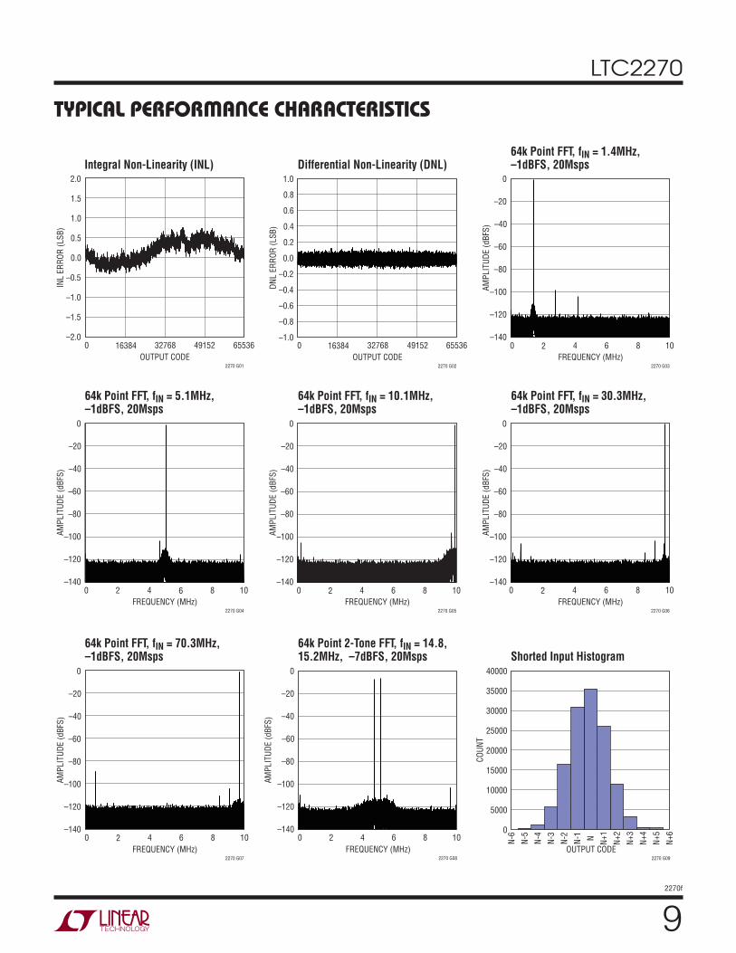
TYPICAL PERFORMANCE CHARACTERISTICS
Integral Non-Linearity (INL) Differential Non-Linearity (DNL)64k Point FFT, fIN = 1.4MHz, –1dBFS, 20Msps
OUTPUT CODE0
–2.0
–1.5
–1.0
INL
ERRO
R (L
SB)
–0.5
0.5
0.0
1.0
1.5
2.0
16384 32768 49152 65536
2270 G01
OUTPUT CODE
–1.0
–0.4
–0.2
–0.6
–0.8
DN
L E
RR
OR
(LS
B)
0.0
0.4
0.2
0.6
0.8
1.0
2270 G02
0 16384 32768 49152 65536
FREQUENCY (MHz)
–100
–140
–120
–60
–80
AM
PLIT
UD
E (
dB
FS) –40
0
–20
2270 G03
0 2 64 108
64k Point FFT, fIN = 5.1MHz, –1dBFS, 20Msps
64k Point FFT, fIN = 10.1MHz, –1dBFS, 20Msps
64k Point FFT, fIN = 30.3MHz, –1dBFS, 20Msps
64k Point FFT, fIN = 70.3MHz, –1dBFS, 20Msps
64k Point 2-Tone FFT, fIN = 14.8, 15.2MHz, –7dBFS, 20Msps
FREQUENCY (MHz)
–100
–140
–120
–60
–80
AM
PLIT
UD
E (
dB
FS) –40
–20
0
2270 G04
0 2 4 6 8 10FREQUENCY (MHz)
–100
–140
–120
–60
–80
AM
PLIT
UD
E (
dB
FS) –40
–20
0
2270 G05
0 2 864 10FREQUENCY (MHz)
–100
–120
–140
–60
–80
AM
PLIT
UD
E (
dB
FS) –40
–20
0
2270 G06
0 2 64 108
FREQUENCY (MHz)
0
–120
–140
–80
–100AM
PLIT
UD
E (
dB
FS)
–60
0
–20
–40
2 4 6 8 10
2270 G08
OUTPUT CODE
N-6
10000
5000
0
40000
35000
30000
25000
20000
15000
CO
UN
T
N-5
N-4
N-3
N-2
N-1
N+6
N+5
N+4
N+3
N+2
N+1
N
2270 G09
Shorted Input Histogram
FREQUENCY (MHz)0
–100
–120
–140
–60
–80
AMPL
ITUD
E (d
BFS) –40
–20
0
2 64 108
2270 G07
LTC2270
102270f
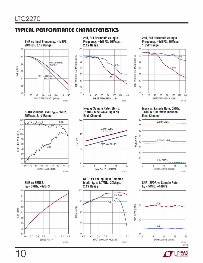
TYPICAL PERFORMANCE CHARACTERISTICS
SFDR vs Input Level, fIN = 5MHz, 20Msps, 2.1V Range
INPUT FREQUENCY (MHz)
0
85
80
75
70
90
2N
D A
ND
3R
D H
AR
MO
NIC
(dB
FS)
95
105
100
20 40 60 80 100 120 140
2270 G12
2ND
3RD
INPUT LEVEL (dBFS)
–8040
60
50
80
70
130
120
110
100
90
SFD
R (
dB
c A
ND
dB
FS)
–70 –40–50–60 0–10–20–30
2270 G13
dBFS
dBc
0 20 40 60 80 100 120 140
INPUT FREQUENCY (MHz)
83
82
81
80
79
85
84
SN
R (
dB
FS)
2270 G10
SINGLE-ENDEDENCODE
DIFFERENTIALENCODE
SNR vs Input Frequency, –1dBFS, 20Msps, 2.1V Range
IVDD vs Sample Rate, 5MHz, –1dBFS Sine Wave Input on Each Channel
IOVDD vs Sample Rate, 5MHz, –1dBFS Sine Wave Input on Each Channel
SNR, SFDR vs Sample Rate, fIN = 5MHz, –1dBFS
SFDR vs Analog Input Common Mode, fIN = 9.7MHz, 20Msps, 2.1V Range
SNR vs SENSE, fIN = 5MHz, –1dBFS
SAMPLE RATE (Msps)
0
80
70
90
100
I VD
D (
mA
)
5 10 15 20
2270 G14
3.5mA LVDSOUTPUTS
CMOS OUTPUTS
SAMPLE RATE (Msps)
0
10
0
20
30
80
70
60
50
40
I OV
DD
(m
A)
5 10 15 20
2270 G15
3.5mA LVDS
1.75mA LVDS
1.8V CMOS
SENSE PIN (V)
0.677
78
79
80SN
R (
dB
FS)
81
82
85
84
83
0.80.7 1 1.21.10.9 1.3
2270 G16
80
85
SFD
R (
dB
FS)
90
95
100
2270 G17
INPUT COMMON MODE (V)
0.6 0.80.7 0.9 1.11 1.2
VDD 1.9V
VDD 1.7V
SAMPLE RATE (Msps)
080
90SN
R, S
FDR
(dB
FS)
100
110
105 15 20
2270 G18
SFDR
SNR
0 20 6040 80 100 120 140
INPUT FREQUENCY (MHz)
95
90
85
80
75
70
105
100
2N
D A
ND
3R
D H
AR
MO
NIC
(dB
FS)
2270 G11
2ND
3RD
2nd, 3rd Harmonic vs Input Frequency, –1dBFS, 20Msps, 2.1V Range
2nd, 3rd Harmonic vs Input Frequency, –1dBFS, 20Msps, 1.05V Range
112270f
LTC2270
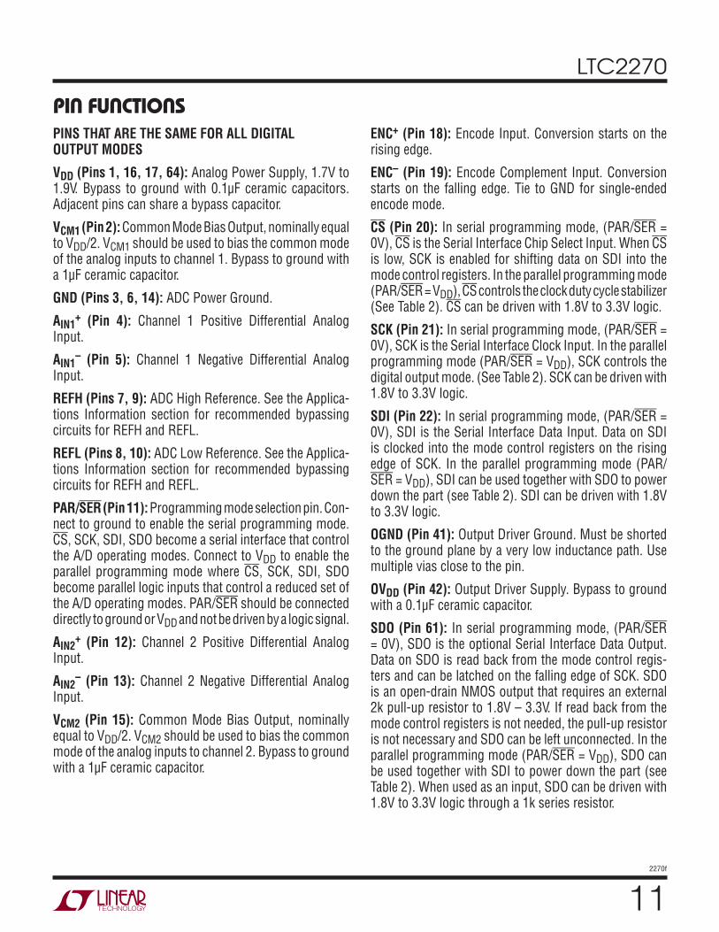
PINS THAT ARE THE SAME FOR ALL DIGITAL OUTPUT MODES
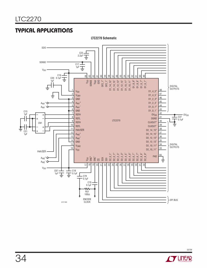
VDD (Pins 1, 16, 17, 64): Analog Power Supply, 1.7V to 1.9V. Bypass to ground with 0.1μF ceramic capacitors. Adjacent pins can share a bypass capacitor.
VCM1 (Pin 2): Common Mode Bias Output, nominally equal to VDD/2. VCM1 should be used to bias the common mode of the analog inputs to channel 1. Bypass to ground with a 1μF ceramic capacitor.
GND (Pins 3, 6, 14): ADC Power Ground.
AIN1+ (Pin 4): Channel 1 Positive Differential Analog
Input.
AIN1– (Pin 5): Channel 1 Negative Differential Analog
Input.
REFH (Pins 7, 9): ADC High Reference. See the Applica-tions Information section for recommended bypassing circuits for REFH and REFL.
REFL (Pins 8, 10): ADC Low Reference. See the Applica-tions Information section for recommended bypassing circuits for REFH and REFL.
PAR/SER (Pin 11): Programming mode selection pin. Con-nect to ground to enable the serial programming mode. CS, SCK, SDI, SDO become a serial interface that control the A/D operating modes. Connect to VDD to enable the parallel programming mode where CS, SCK, SDI, SDO become parallel logic inputs that control a reduced set of the A/D operating modes. PAR/SER should be connected directly to ground or VDD and not be driven by a logic signal.
AIN2+ (Pin 12): Channel 2 Positive Differential Analog
Input.
AIN2– (Pin 13): Channel 2 Negative Differential Analog
Input.
VCM2 (Pin 15): Common Mode Bias Output, nominally equal to VDD/2. VCM2 should be used to bias the common mode of the analog inputs to channel 2. Bypass to ground with a 1μF ceramic capacitor.
ENC+ (Pin 18): Encode Input. Conversion starts on the rising edge.
ENC– (Pin 19): Encode Complement Input. Conversion starts on the falling edge. Tie to GND for single-ended encode mode.
CS (Pin 20): In serial programming mode, (PAR/SER = 0V), CS is the Serial Interface Chip Select Input. When CS is low, SCK is enabled for shifting data on SDI into the mode control registers. In the parallel programming mode (PAR/SER = VDD), CS controls the clock duty cycle stabilizer (See Table 2). CS can be driven with 1.8V to 3.3V logic.
SCK (Pin 21): In serial programming mode, (PAR/SER = 0V), SCK is the Serial Interface Clock Input. In the parallel programming mode (PAR/SER = VDD), SCK controls the digital output mode. (See Table 2). SCK can be driven with 1.8V to 3.3V logic.
SDI (Pin 22): In serial programming mode, (PAR/SER = 0V), SDI is the Serial Interface Data Input. Data on SDI is clocked into the mode control registers on the rising edge of SCK. In the parallel programming mode (PAR/SER = VDD), SDI can be used together with SDO to power down the part (see Table 2). SDI can be driven with 1.8V to 3.3V logic.
OGND (Pin 41): Output Driver Ground. Must be shorted to the ground plane by a very low inductance path. Use multiple vias close to the pin.
OVDD (Pin 42): Output Driver Supply. Bypass to ground with a 0.1μF ceramic capacitor.
SDO (Pin 61): In serial programming mode, (PAR/SER = 0V), SDO is the optional Serial Interface Data Output. Data on SDO is read back from the mode control regis-ters and can be latched on the falling edge of SCK. SDO is an open-drain NMOS output that requires an external 2k pull-up resistor to 1.8V – 3.3V. If read back from the mode control registers is not needed, the pull-up resistor is not necessary and SDO can be left unconnected. In the parallel programming mode (PAR/SER = VDD), SDO can be used together with SDI to power down the part (see Table 2). When used as an input, SDO can be driven with 1.8V to 3.3V logic through a 1k series resistor.
PIN FUNCTIONS
LTC2270
122270f
PIN FUNCTIONSVREF (Pin 62): Reference Voltage Output. Bypass to ground with a 2.2μF ceramic capacitor. The output voltage is nominally 1.25V.
SENSE (Pin 63): Reference Programming Pin. Connecting SENSE to VDD selects the internal reference and a ±1.05V input range. Connecting SENSE to ground selects the internal reference and a ±0.525V input range. An external reference between 0.625V and 1.3V applied to SENSE selects an input range of ±0.84 • VSENSE.
Ground (Exposed Pad Pin 65): The exposed pad must be soldered to the PCB ground.
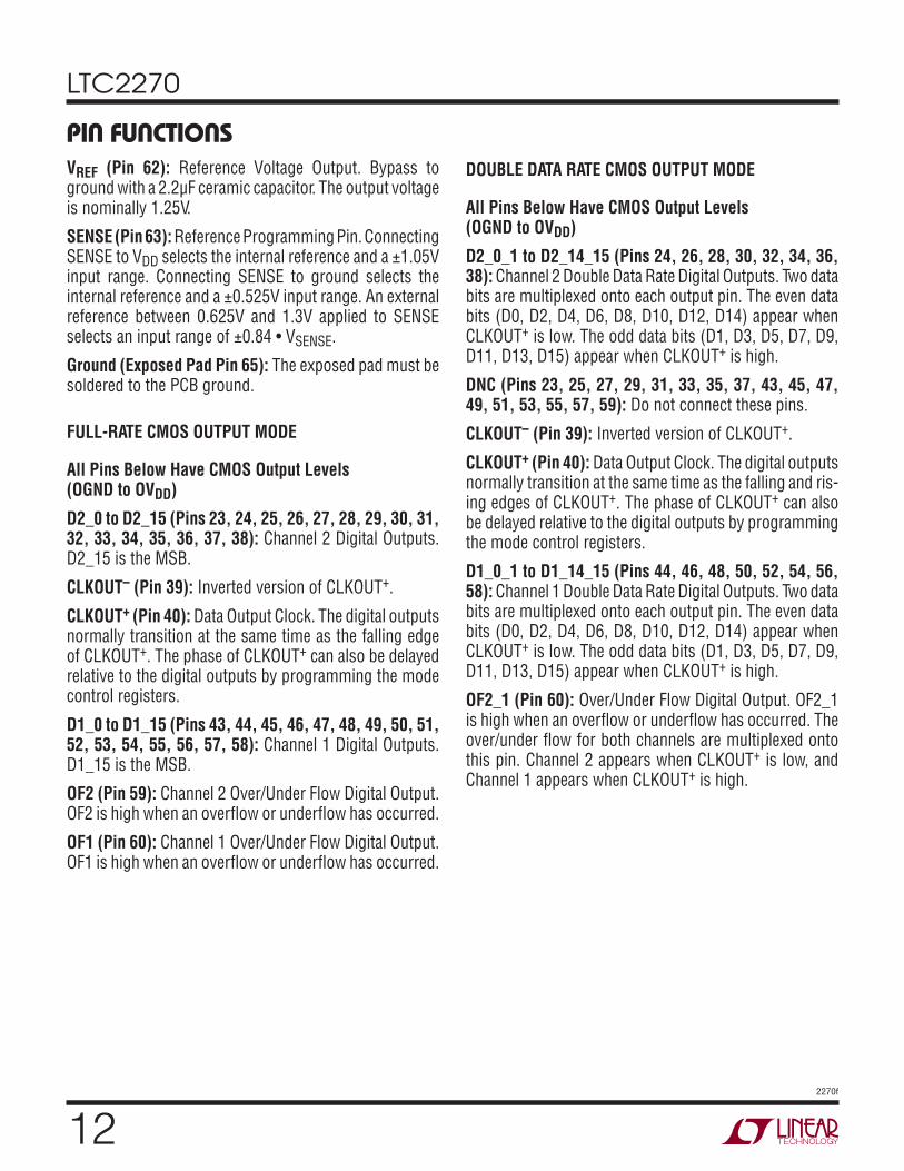
FULL-RATE CMOS OUTPUT MODE
All Pins Below Have CMOS Output Levels (OGND to OVDD)
D2_0 to D2_15 (Pins 23, 24, 25, 26, 27, 28, 29, 30, 31, 32, 33, 34, 35, 36, 37, 38): Channel 2 Digital Outputs. D2_15 is the MSB.
CLKOUT– (Pin 39): Inverted version of CLKOUT+.
CLKOUT+ (Pin 40): Data Output Clock. The digital outputs normally transition at the same time as the falling edge of CLKOUT+. The phase of CLKOUT+ can also be delayed relative to the digital outputs by programming the mode control registers.
D1_0 to D1_15 (Pins 43, 44, 45, 46, 47, 48, 49, 50, 51, 52, 53, 54, 55, 56, 57, 58): Channel 1 Digital Outputs. D1_15 is the MSB.
OF2 (Pin 59): Channel 2 Over/Under Flow Digital Output. OF2 is high when an overflow or underflow has occurred.
OF1 (Pin 60): Channel 1 Over/Under Flow Digital Output. OF1 is high when an overflow or underflow has occurred.
DOUBLE DATA RATE CMOS OUTPUT MODE
All Pins Below Have CMOS Output Levels (OGND to OVDD)
D2_0_1 to D2_14_15 (Pins 24, 26, 28, 30, 32, 34, 36, 38): Channel 2 Double Data Rate Digital Outputs. Two data bits are multiplexed onto each output pin. The even data bits (D0, D2, D4, D6, D8, D10, D12, D14) appear when CLKOUT+ is low. The odd data bits (D1, D3, D5, D7, D9, D11, D13, D15) appear when CLKOUT+ is high.
DNC (Pins 23, 25, 27, 29, 31, 33, 35, 37, 43, 45, 47, 49, 51, 53, 55, 57, 59): Do not connect these pins.
CLKOUT– (Pin 39): Inverted version of CLKOUT+.
CLKOUT+ (Pin 40): Data Output Clock. The digital outputs normally transition at the same time as the falling and ris-ing edges of CLKOUT+. The phase of CLKOUT+ can also be delayed relative to the digital outputs by programming the mode control registers.
D1_0_1 to D1_14_15 (Pins 44, 46, 48, 50, 52, 54, 56, 58): Channel 1 Double Data Rate Digital Outputs. Two data bits are multiplexed onto each output pin. The even data bits (D0, D2, D4, D6, D8, D10, D12, D14) appear when CLKOUT+ is low. The odd data bits (D1, D3, D5, D7, D9, D11, D13, D15) appear when CLKOUT+ is high.
OF2_1 (Pin 60): Over/Under Flow Digital Output. OF2_1 is high when an overflow or underflow has occurred. The over/under flow for both channels are multiplexed onto this pin. Channel 2 appears when CLKOUT+ is low, and Channel 1 appears when CLKOUT+ is high.
132270f
LTC2270
DOUBLE DATA RATE LVDS OUTPUT MODE
All Pins Below Have LVDS Output Levels. The Output Current Level Is Programmable. There Is an Optional Internal 100Ω Termination Resistor Between the Pins of Each LVDS Output Pair.
D2_0_1–/D2_0_1+ to D2_14_15–/D2_14_15+ (Pins 23/24, 25/26, 27/28, 29/30, 31/32, 33/34, 35/36, 37/38): Chan-nel 2 Double Data Rate Digital Outputs. Two data bits are multiplexed onto each differential output pair. The even data bits (D0, D2, D4, D6, D8, D10, D12, D14) appear when CLKOUT+ is low. The odd data bits (D1, D3, D5, D7, D9, D11, D13, D15) appear when CLKOUT+ is high.
CLKOUT–/CLKOUT+ (Pins 39/40): Data Output Clock. The digital outputs normally transition at the same time as the falling and rising edges of CLKOUT+. The phase of
CLKOUT+ can also be delayed relative to the digital outputs by programming the mode control registers.
D1_0_1–/D1_0_1+ to D1_14_15–/D1_14_15+ (Pins 43/44, 45/46, 47/48, 49/50, 51/52, 53/54, 55/56, 57/58): Chan-nel 1 Double Data Rate Digital Outputs. Two data bits are multiplexed onto each differential output pair. The even data bits (D0, D2, D4, D6, D8, D10, D12, D14) appear when CLKOUT+ is low. The odd data bits (D1, D3, D5, D7, D9, D11, D13, D15) appear when CLKOUT+ is high.
OF2_1–/OF2_1+ (Pins 59/60): Over/Under Flow Digital Output. OF2_1+ is high when an overflow or underflow has occurred. The over/under flow for both channels are multiplexed onto this pin. Channel 2 appears when CLKOUT+ is low, and Channel 1 appears when CLKOUT+ is high.
PIN FUNCTIONS
LTC2270
142270f
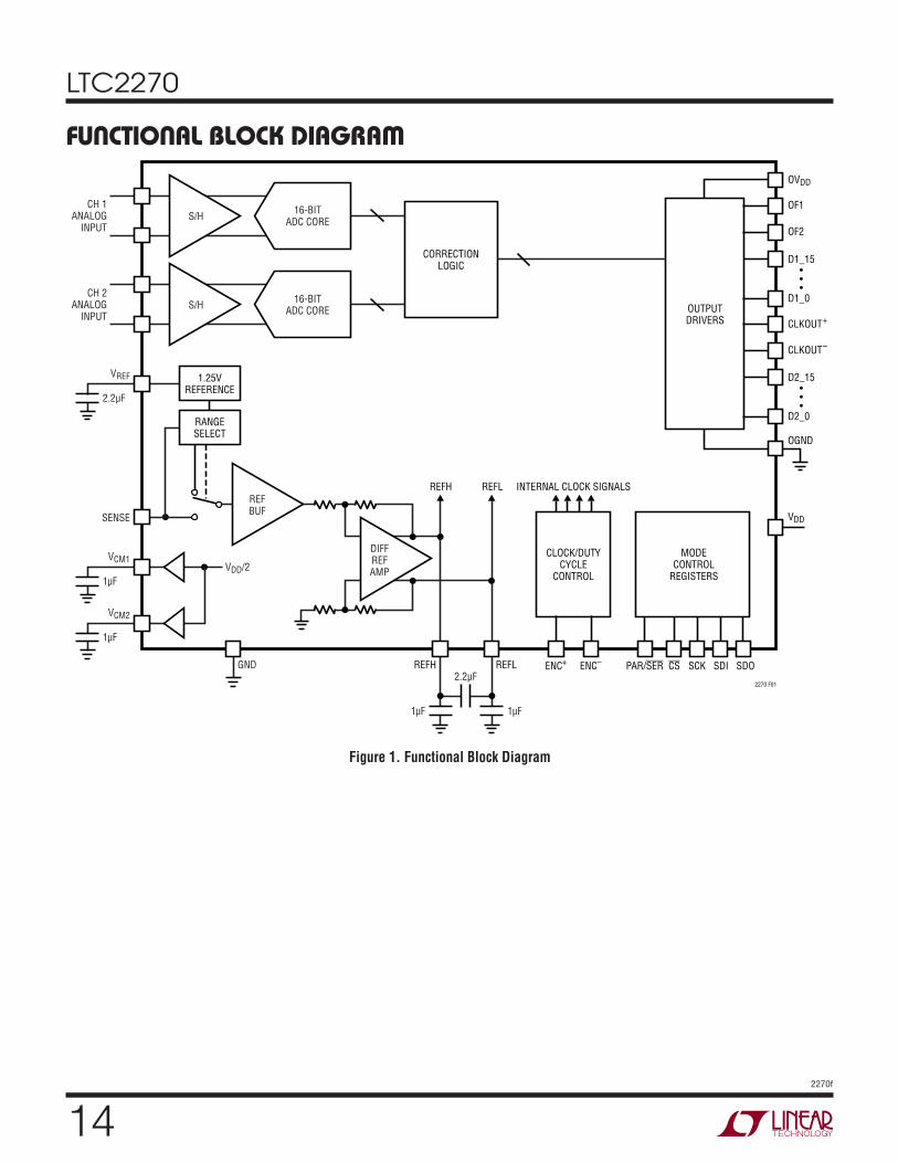
FUNCTIONAL BLOCK DIAGRAM
DIFFREFAMP
REFBUF
2.2μF
1μF 1μF
INTERNAL CLOCK SIGNALSREFH REFL
CLOCK/DUTYCYCLE
CONTROL
RANGESELECT
1.25VREFERENCE
ENC+REFH REFL ENC–
CORRECTIONLOGIC
SDOCS
OGND
OF1
OVDD
D1_15
CLKOUT–
CLKOUT+
D1_0
2270 F01
SENSE
VREF
CH 1ANALOG
INPUT
2.2μF
VCM1
1μF
VDD/2
OUTPUTDRIVERS
MODECONTROL
REGISTERS
SCKPAR/SER SDIGND
S/H16-BIT
ADC CORE
CH 2ANALOG
INPUTS/H
16-BITADC CORE
VCM2
1μF
OF2
D2_15
D2_0
VDD
Figure 1. Functional Block Diagram
152270f
LTC2270
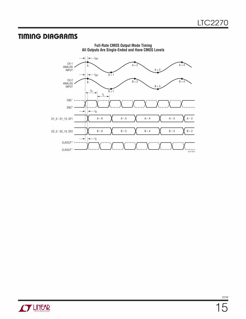
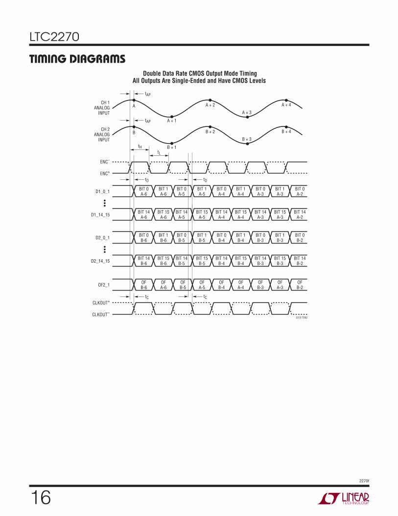
Full-Rate CMOS Output Mode Timing All Outputs Are Single-Ended and Have CMOS Levels
TIMING DIAGRAMS
tH
tD
tC
tL
B – 6 B – 5 B – 4 B – 3 B – 2
tAP
A + 1
A + 2 A + 4
A + 3
ACH 1
ANALOGINPUT
ENC–
ENC+
CLKOUT+
CLKOUT–
D2_0 - D2_15, OF2
tAP
B + 1
B + 2 B + 4
B + 3
BCH 2
ANALOGINPUT
A – 6 A – 5 A – 4 A – 3 A – 2D1_0 - D1_15, OF1
2270 TD01
LTC2270
162270f
TIMING DIAGRAMS Double Data Rate CMOS Output Mode Timing
All Outputs Are Single-Ended and Have CMOS Levels
tD tD
tC tC
tL
BIT 0A-6
BIT 1A-6
BIT 0A-5
BIT 1A-5
BIT 0A-4
BIT 1A-4
BIT 0A-3
BIT 1A-3
BIT 0A-2
BIT 14A-6
BIT 15A-6
BIT 14A-5
BIT 15A-5
BIT 14A-4
BIT 15A-4
BIT 14A-3
BIT 15A-3
BIT 14A-2
ENC–
ENC+
D1_0_1
D1_14_15
BIT 0B-6
BIT 1B-6
BIT 0B-5
BIT 1B-5
BIT 0B-4
BIT 1B-4
BIT 0B-3
BIT 1B-3
BIT 0B-2
BIT 14B-6
BIT 15B-6
BIT 14B-5
BIT 15B-5
BIT 14B-4
BIT 15B-4
BIT 14B-3
BIT 15B-3
BIT 14B-2
OFB-6
OFA-6
OFB-5
OFA-5
OFB-4
OFA-4
OFB-3
OFA-3
OFB-2
D2_0_1
D2_14_15
CLKOUT+
CLKOUT–
OF2_1
2270 TD02
tH
tAP
A + 1
A + 2 A + 4
A + 3
ACH 1
ANALOGINPUT
tAP
B + 1
B + 2 B + 4
B + 3
BCH 2
ANALOGINPUT
172270f
LTC2270
TIMING DIAGRAMS Double Data Rate LVDS Output Mode Timing
All Outputs Are Differential and Have LVDS Levels
tD tD
tC tC
tL
BIT 0A-6
BIT 1A-6
BIT 0A-5
BIT 1A-5
BIT 0A-4
BIT 1A-4
BIT 0A-3
BIT 1A-3
BIT 0A-2
BIT 14A-6
BIT 15A-6
BIT 14A-5
BIT 15A-5
BIT 14A-4
BIT 15A-4
BIT 14A-3
BIT 15A-3
BIT 14A-2
ENC–
ENC+
D1_0_1+
D1_14_15+
BIT 0B-6
BIT 1B-6
BIT 0B-5
BIT 1B-5
BIT 0B-4
BIT 1B-4
BIT 0B-3
BIT 1B-3
BIT 0B-2
BIT 14B-6
BIT 15B-6
BIT 14B-5
BIT 15B-5
BIT 14B-4
BIT 15B-4
BIT 14B-3
BIT 15B-3
BIT 14B-2
OFB-6
OFA-6
OFB-5
OFA-5
OFB-4
OFA-4
OFB-3
OFA-3
OFB-2
D2_0_1+
D2_14_15+
CLKOUT+
CLKOUT–
OF2_1+
D1_0_1–
D1_14_15–
D2_0_1–
D2_14_15–
OF2_1–
2270 TD03
tH
tAP
A + 1
A + 2 A + 4
A + 3
ACH 1
ANALOGINPUT
tAP
B + 1
B + 2 B + 4
B + 3
BCH 2
ANALOGINPUT
LTC2270
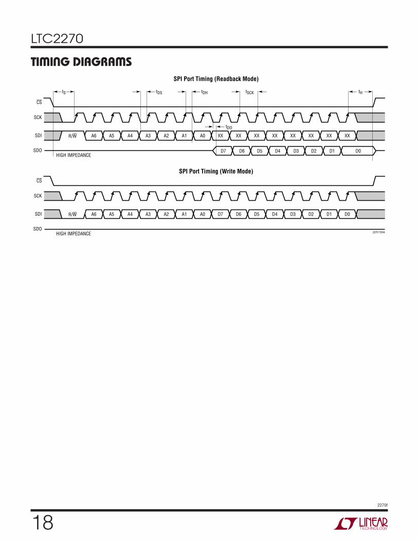
182270f
A6
tS tDS
A5 A4 A3 A2 A1 A0 XX
D7 D6 D5 D4 D3 D2 D1 D0
XX XX XX XX XX XX XX
CS
SCK
SDI R/W
SDOHIGH IMPEDANCE
SPI Port Timing (Readback Mode)
SPI Port Timing (Write Mode)
tDH
tDO
tSCK tH
A6 A5 A4 A3 A2 A1 A0 D7 D6 D5 D4 D3 D2 D1 D0
2270 TD04
CS
SCK
SDI R/W
SDOHIGH IMPEDANCE
TIMING DIAGRAMS
192270f
LTC2270
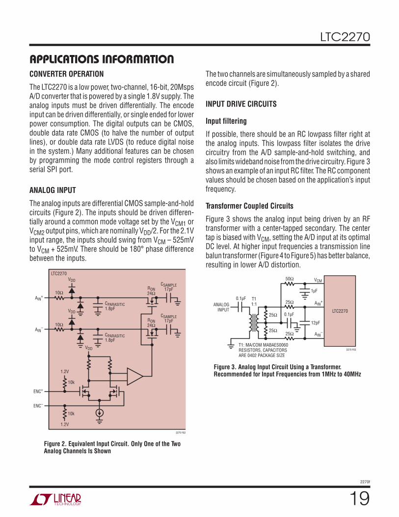
CONVERTER OPERATION
The LTC2270 is a low power, two-channel, 16-bit, 20Msps A/D converter that is powered by a single 1.8V supply. The analog inputs must be driven differentially. The encode input can be driven differentially, or single ended for lower power consumption. The digital outputs can be CMOS, double data rate CMOS (to halve the number of output lines), or double data rate LVDS (to reduce digital noise in the system.) Many additional features can be chosen by programming the mode control registers through a serial SPI port.
ANALOG INPUT
The analog inputs are differential CMOS sample-and-hold circuits (Figure 2). The inputs should be driven differen-tially around a common mode voltage set by the VCM1 or VCM2 output pins, which are nominally VDD/2. For the 2.1V input range, the inputs should swing from VCM – 525mV to VCM + 525mV. There should be 180° phase difference between the inputs.
The two channels are simultaneously sampled by a shared encode circuit (Figure 2).
INPUT DRIVE CIRCUITS
Input filtering
If possible, there should be an RC lowpass filter right at the analog inputs. This lowpass filter isolates the drive circuitry from the A/D sample-and-hold switching, and also limits wideband noise from the drive circuitry. Figure 3 shows an example of an input RC filter. The RC component values should be chosen based on the application’s input frequency.
Transformer Coupled Circuits
Figure 3 shows the analog input being driven by an RF transformer with a center-tapped secondary. The center tap is biased with VCM, setting the A/D input at its optimal DC level. At higher input frequencies a transmission line balun transformer (Figure 4 to Figure 5) has better balance, resulting in lower A/D distortion.
CSAMPLE17pFRON
24Ω
RON24Ω
VDD
VDD
LTC2270
AIN+
2270 F02
CSAMPLE17pF
VDD
AIN–
ENC–
ENC+
1.2V
10k
1.2V
10k
CPARASITIC1.8pF
CPARASITIC1.8pF
10Ω
10Ω
25Ω
25Ω25Ω
25Ω
50Ω
0.1μF
AIN+
AIN–
12pF
1μF
VCM
LTC2270
ANALOGINPUT
0.1μF T11:1
T1: MA/COM MABAES0060RESISTORS, CAPACITORS ARE 0402 PACKAGE SIZE
2270 F03
Figure 2. Equivalent Input Circuit. Only One of the Two Analog Channels Is Shown
Figure 3. Analog Input Circuit Using a Transformer. Recommended for Input Frequencies from 1MHz to 40MHz
APPLICATIONS INFORMATION
LTC2270
202270f
APPLICATIONS INFORMATION
Figure 5. Recommended Front-End Circuit for Input Frequencies Above 80MHz
Amplifier Circuits
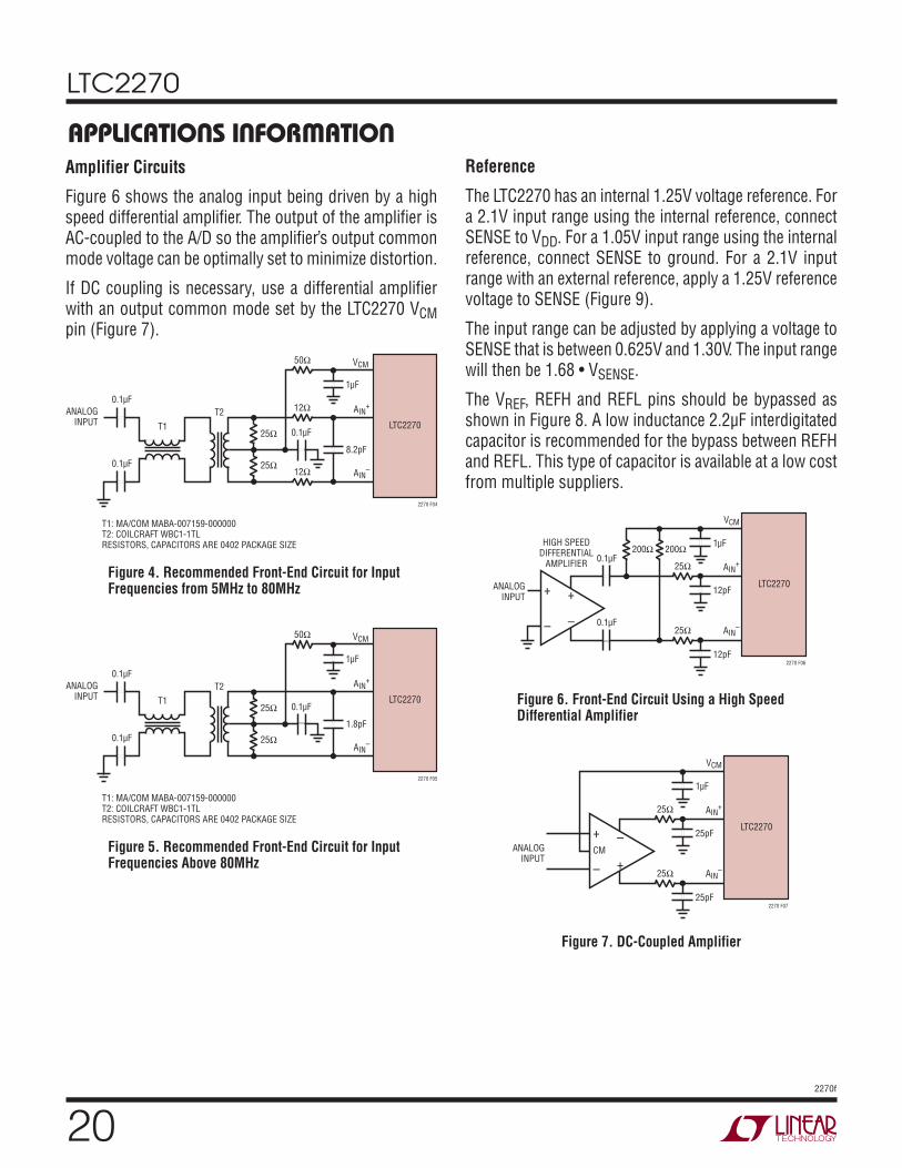
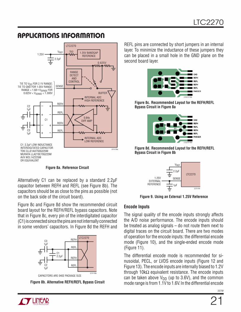
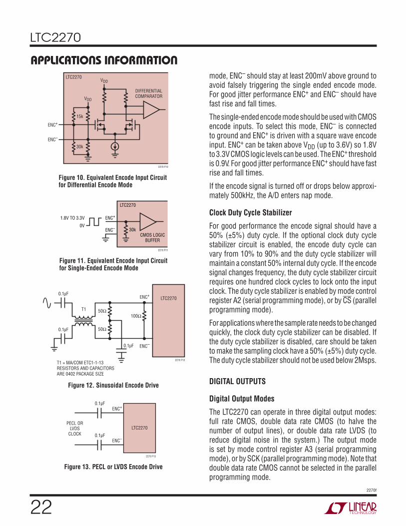
Figure 6 shows the analog input being driven by a high speed differential amplifier. The output of the amplifier is AC-coupled to the A/D so the amplifier’s output common mode voltage can be optimally set to minimize distortion.
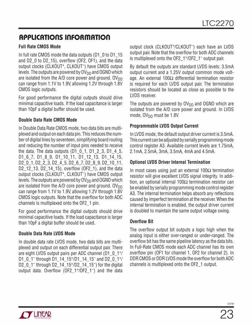
If DC coupling is necessary, use a differential amplifier with an output common mode set by the LTC2270 VCM pin (Figure 7).
Figure 4. Recommended Front-End Circuit for Input Frequencies from 5MHz to 80MHz
Reference
The LTC2270 has an internal 1.25V voltage reference. For a 2.1V input range using the internal reference, connect SENSE to VDD. For a 1.05V input range using the internal reference, connect SENSE to ground. For a 2.1V input range with an external reference, apply a 1.25V reference voltage to SENSE (Figure 9).
The input range can be adjusted by applying a voltage to SENSE that is between 0.625V and 1.30V. The input range will then be 1.68 • VSENSE.
The VREF, REFH and REFL pins should be bypassed as shown in Figure 8. A low inductance 2.2μF interdigitated capacitor is recommended for the bypass between REFH and REFL. This type of capacitor is available at a low cost from multiple suppliers.
25Ω
12Ω
12Ω25Ω
50Ω
0.1μF
AIN+
AIN–
8.2pF
1μF
VCM
ANALOGINPUT
0.1μF
0.1μF
T1
T2
T1: MA/COM MABA-007159-000000T2: COILCRAFT WBC1-1TL RESISTORS, CAPACITORS ARE 0402 PACKAGE SIZE
2270 F04
LTC2270
25Ω
25Ω
50Ω
0.1μF
AIN+
AIN–
1.8pF
1μF
VCM
ANALOGINPUT
0.1μF
0.1μF
T1
T2
T1: MA/COM MABA-007159-000000T2: COILCRAFT WBC1-1TL RESISTORS, CAPACITORS ARE 0402 PACKAGE SIZE
2270 F05
LTC2270
25Ω
25Ω
200Ω200Ω0.1μF
AIN+
AIN–
1μF
12pF
12pF
VCM
LTC2270
2270 F06
– –
+ +ANALOG
INPUT
HIGH SPEEDDIFFERENTIAL
AMPLIFIER
0.1μF
25Ω
25Ω AIN+
AIN–
1μF
25pF
25pF
VCM
LTC2270
2270 F07
– +
+ –ANALOG
INPUTCM
Figure 6. Front-End Circuit Using a High Speed Differential Amplifier
Figure 7. DC-Coupled Amplifier
212270f
LTC2270
APPLICATIONS INFORMATION
VREF
REFH
REFH
SENSE
C1
TIE TO VDD FOR 2.1V RANGE;TIE TO GND FOR 1.05V RANGE;
SENSE FOR0.625V < VSENSE < 1.300V
1.25V
REFL
REFL
INTERNAL ADCHIGH REFERENCE
BUFFER
2270 F08a
LTC2270
5Ω
0.84xDIFF AMP
INTERNAL ADCLOW REFERENCE
C1: 2.2μF LOW INDUCTANCE INTERDIGITATED CAPACITORTDK CLLE1AX7S0G225MMURATA LLA219C70G225MAVX W2L14Z225MOR EQUIVALENT
1.25V BANDGAPREFERENCE
0.625V
RANGEDETECT
ANDCONTROL
2.2μF
C21μF
C31μF
+
+
–
–
–
–
+
+
Figure 8a. Reference Circuit
SENSE1.25VEXTERNAL
REFERENCE
2.2μF
1μF
VREF
2270 F09
LTC2270
Figure 9. Using an External 1.25V Reference
REFH
REFH
REFL
REFL
2270 F08b
LTC2270
CAPACITORS ARE 0402 PACKAGE SIZE
C31μF
C12.2μF
C21μF
Figure 8b. Alternative REFH/REFL Bypass Circuit
Figure 8c. Recommended Layout for the REFH/REFL Bypass Circuit in Figure 8a
Alternatively C1 can be replaced by a standard 2.2μF capacitor between REFH and REFL (see Figure 8b). The capacitors should be as close to the pins as possible (not on the back side of the circuit board).
Figure 8c and Figure 8d show the recommended circuit board layout for the REFH/REFL bypass capacitors. Note that in Figure 8c, every pin of the interdigitated capacitor (C1) is connected since the pins are not internally connected in some vendors’ capacitors. In Figure 8d the REFH and
Figure 8d. Recommended Layout for the REFH/REFL Bypass Circuit in Figure 8b
Encode Inputs
The signal quality of the encode inputs strongly affects the A/D noise performance. The encode inputs should be treated as analog signals – do not route them next to digital traces on the circuit board. There are two modes of operation for the encode inputs: the differential encode mode (Figure 10), and the single-ended encode mode (Figure 11).
The differential encode mode is recommended for si-nusoidal, PECL, or LVDS encode inputs (Figure 12 and Figure 13). The encode inputs are internally biased to 1.2V through 10kΩ equivalent resistance. The encode inputs can be taken above VDD (up to 3.6V), and the common mode range is from 1.1V to 1.6V. In the differential encode
REFL pins are connected by short jumpers in an internal layer. To minimize the inductance of these jumpers they can be placed in a small hole in the GND plane on the second board layer.
LTC2270 F08c
LTC2270 F08d
LTC2270
222270f
50Ω100Ω
0.1μF
T1 = MA/COM ETC1-1-13
RESISTORS AND CAPACITORS
ARE 0402 PACKAGE SIZE
50Ω
LTC2270
2270 F12
ENC–
ENC+
0.1μF
0.1μF
T1
Figure 12. Sinusoidal Encode Drive
ENC+
ENC–
PECL ORLVDS
CLOCK
0.1μF
0.1μF
2270 F13
LTC2270
Figure 13. PECL or LVDS Encode Drive
VDDLTC2270
2270 F10
ENC–
ENC+
15k
VDD
DIFFERENTIALCOMPARATOR
30k
Figure 10. Equivalent Encode Input Circuit for Differential Encode Mode
30k
ENC+
ENC–
2270 F11
0V
1.8V TO 3.3V
LTC2270
CMOS LOGICBUFFER
Figure 11. Equivalent Encode Input Circuit for Single-Ended Encode Mode
mode, ENC– should stay at least 200mV above ground to avoid falsely triggering the single ended encode mode. For good jitter performance ENC+ and ENC– should have fast rise and fall times.
The single-ended encode mode should be used with CMOS encode inputs. To select this mode, ENC– is connected to ground and ENC+ is driven with a square wave encode input. ENC+ can be taken above VDD (up to 3.6V) so 1.8V to 3.3V CMOS logic levels can be used. The ENC+ threshold is 0.9V. For good jitter performance ENC+ should have fast rise and fall times.
If the encode signal is turned off or drops below approxi-mately 500kHz, the A/D enters nap mode.
Clock Duty Cycle Stabilizer
For good performance the encode signal should have a 50% (±5%) duty cycle. If the optional clock duty cycle stabilizer circuit is enabled, the encode duty cycle can vary from 10% to 90% and the duty cycle stabilizer will maintain a constant 50% internal duty cycle. If the encode signal changes frequency, the duty cycle stabilizer circuit requires one hundred clock cycles to lock onto the input clock. The duty cycle stabilizer is enabled by mode control register A2 (serial programming mode), or by CS (parallel programming mode).
For applications where the sample rate needs to be changed quickly, the clock duty cycle stabilizer can be disabled. If the duty cycle stabilizer is disabled, care should be taken to make the sampling clock have a 50% (±5%) duty cycle. The duty cycle stabilizer should not be used below 2Msps.
DIGITAL OUTPUTS
Digital Output Modes
The LTC2270 can operate in three digital output modes: full rate CMOS, double data rate CMOS (to halve the number of output lines), or double data rate LVDS (to reduce digital noise in the system.) The output mode is set by mode control register A3 (serial programming mode), or by SCK (parallel programming mode). Note that double data rate CMOS cannot be selected in the parallel programming mode.
APPLICATIONS INFORMATION
232270f
LTC2270
APPLICATIONS INFORMATIONFull Rate CMOS Mode
In full rate CMOS mode the data outputs (D1_0 to D1_15 and D2_0 to D2_15), overflow (OF2, OF1), and the data output clocks (CLKOUT+, CLKOUT–) have CMOS output levels. The outputs are powered by OVDD and OGND which are isolated from the A/D core power and ground. OVDD can range from 1.1V to 1.9V, allowing 1.2V through 1.8V CMOS logic outputs.
For good performance the digital outputs should drive minimal capacitive loads. If the load capacitance is larger than 10pF a digital buffer should be used.
Double Data Rate CMOS Mode
In Double Data Rate CMOS mode, two data bits are multi-plexed and output on each data pin. This reduces the num-ber of digital lines by seventeen, simplifying board routing and reducing the number of input pins needed to receive the data. The data outputs (D1_0_1, D1_2_3, D1_4_5, D1_6_7, D1_8_9, D1_10_11, D1_12_13, D1_14_15, D2_0_1, D2_2_3, D2_4_5, D2_6_7, D2_8_9, D2_10_11, D2_12_13, D2_14_15), overflow (OF2_1), and the data output clocks (CLKOUT+, CLKOUT–) have CMOS output levels. The outputs are powered by OVDD and OGND which are isolated from the A/D core power and ground. OVDD can range from 1.1V to 1.9V, allowing 1.2V through 1.8V CMOS logic outputs. Note that the overflow for both ADC channels is multiplexed onto the OF2_1 pin.
For good performance the digital outputs should drive minimal capacitive loads. If the load capacitance is larger than 10pF a digital buffer should be used.
Double Data Rate LVDS Mode
In double data rate LVDS mode, two data bits are multi-plexed and output on each differential output pair. There are eight LVDS output pairs per ADC channel (D1_0_1+/D1_0_1– through D1_14_15+/D1_14_15– and D2_0_1+/D2_0_1– through D2_14_15+/D2_14_15–) for the digital output data. Overflow (OF2_1+/OF2_1–) and the data
output clock (CLKOUT+/CLKOUT–) each have an LVDS output pair. Note that the overflow for both ADC channels is multiplexed onto the OF2_1+/OF2_1– output pair.
By default the outputs are standard LVDS levels: 3.5mA output current and a 1.25V output common mode volt-age. An external 100Ω differential termination resistor is required for each LVDS output pair. The termination resistors should be located as close as possible to the LVDS receiver.
The outputs are powered by OVDD and OGND which are isolated from the A/D core power and ground. In LVDS mode, OVDD must be 1.8V.
Programmable LVDS Output Current
In LVDS mode, the default output driver current is 3.5mA. This current can be adjusted by serially programming mode control register A3. Available current levels are 1.75mA, 2.1mA, 2.5mA, 3mA, 3.5mA, 4mA and 4.5mA.
Optional LVDS Driver Internal Termination
In most cases using just an external 100Ω termination resistor will give excellent LVDS signal integrity. In addi-tion, an optional internal 100Ω termination resistor can be enabled by serially programming mode control register A3. The internal termination helps absorb any reflections caused by imperfect termination at the receiver. When the internal termination is enabled, the output driver current is doubled to maintain the same output voltage swing.
Overflow Bit
The overflow output bit outputs a logic high when the analog input is either over-ranged or under-ranged. The overflow bit has the same pipeline latency as the data bits. In Full-Rate CMOS mode each ADC channel has its own overflow pin (OF1 for channel 1, OF2 for channel 2). In DDR CMOS or DDR LVDS mode the overflow for both ADC channels is multiplexed onto the OF2_1 output.
LTC2270
242270f
APPLICATIONS INFORMATIONPhase Shifting the Output Clock
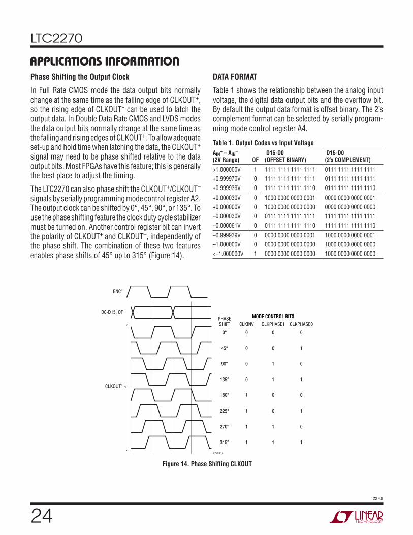
In Full Rate CMOS mode the data output bits normally change at the same time as the falling edge of CLKOUT+, so the rising edge of CLKOUT+ can be used to latch the output data. In Double Data Rate CMOS and LVDS modes the data output bits normally change at the same time as the falling and rising edges of CLKOUT+. To allow adequate set-up and hold time when latching the data, the CLKOUT+ signal may need to be phase shifted relative to the data output bits. Most FPGAs have this feature; this is generally the best place to adjust the timing.
The LTC2270 can also phase shift the CLKOUT+/CLKOUT– signals by serially programming mode control register A2. The output clock can be shifted by 0°, 45°, 90°, or 135°. To use the phase shifting feature the clock duty cycle stabilizer must be turned on. Another control register bit can invert the polarity of CLKOUT+ and CLKOUT–, independently of the phase shift. The combination of these two features enables phase shifts of 45° up to 315° (Figure 14).
DATA FORMAT
Table 1 shows the relationship between the analog input voltage, the digital data output bits and the overflow bit. By default the output data format is offset binary. The 2’s complement format can be selected by serially program-ming mode control register A4.
Table 1. Output Codes vs Input Voltage
AIN+ – AIN
–
(2V Range) OF D15-D0(OFFSET BINARY)
D15-D0(2’s COMPLEMENT)
>1.000000V
+0.999970V
+0.999939V
1
0
0
1111 1111 1111 1111
1111 1111 1111 1111
1111 1111 1111 1110
0111 1111 1111 1111
0111 1111 1111 1111
0111 1111 1111 1110
+0.000030V
+0.000000V
–0.000030V
–0.000061V
0
0
0
0
1000 0000 0000 0001
1000 0000 0000 0000
0111 1111 1111 1111
0111 1111 1111 1110
0000 0000 0000 0001
0000 0000 0000 0000
1111 1111 1111 1111
1111 1111 1111 1110
–0.999939V
–1.000000V
<–1.000000V
0
0
1
0000 0000 0000 0001
0000 0000 0000 0000
0000 0000 0000 0000
1000 0000 0000 0001
1000 0000 0000 0000
1000 0000 0000 0000
CLKOUT+
D0-D15, OF
PHASESHIFT
0°
45°
90°
135°
180°
225°
270°
315°
CLKINV
0
0
0
0
1
1
1
1
CLKPHASE1
MODE CONTROL BITS
0
0
1
1
0
0
1
1
CLKPHASE0
0
1
0
1
0
1
0
1
2270 F14
ENC+
Figure 14. Phase Shifting CLKOUT
252270f
LTC2270
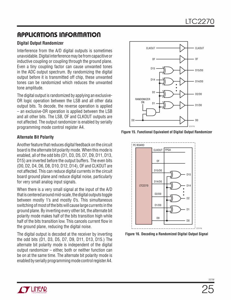
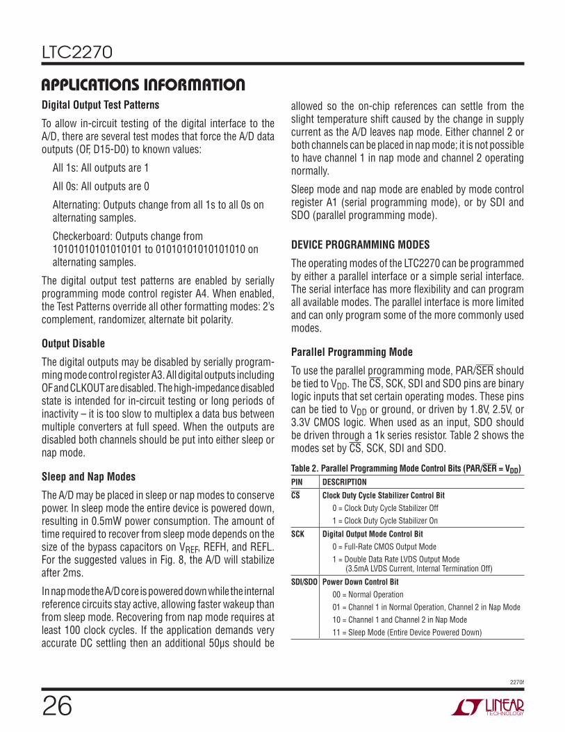
Digital Output Randomizer
Interference from the A/D digital outputs is sometimes unavoidable. Digital interference may be from capacitive or inductive coupling or coupling through the ground plane. Even a tiny coupling factor can cause unwanted tones in the ADC output spectrum. By randomizing the digital output before it is transmitted off chip, these unwanted tones can be randomized which reduces the unwanted tone amplitude.
The digital output is randomized by applying an exclusive-OR logic operation between the LSB and all other data output bits. To decode, the reverse operation is applied – an exclusive-OR operation is applied between the LSB and all other bits. The LSB, OF and CLKOUT outputs are not affected. The output randomizer is enabled by serially programming mode control register A4.
Alternate Bit Polarity
Another feature that reduces digital feedback on the circuit board is the alternate bit polarity mode. When this mode is enabled, all of the odd bits (D1, D3, D5, D7, D9, D11, D13, D15) are inverted before the output buffers. The even bits (D0, D2, D4, D6, D8, D10, D12, D14), OF and CLKOUT are not affected. This can reduce digital currents in the circuit board ground plane and reduce digital noise, particularly for very small analog input signals.
When there is a very small signal at the input of the A/D that is centered around mid-scale, the digital outputs toggle between mostly 1’s and mostly 0’s. This simultaneous switching of most of the bits will cause large currents in the ground plane. By inverting every other bit, the alternate bit polarity mode makes half of the bits transition high while half of the bits transition low. This cancels current flow in the ground plane, reducing the digital noise.
The digital output is decoded at the receiver by inverting the odd bits (D1, D3, D5, D7, D9, D11, D13, D15.) The alternate bit polarity mode is independent of the digital output randomizer – either, both or neither function can be on at the same time. The alternate bit polarity mode is enabled by serially programming mode control register A4.
APPLICATIONS INFORMATION
CLKOUT CLKOUT
OF
D15/D0
D14/D0
D2/D0
D1/D0
D0
2270 F15
OF
D15
D14
D2
D1
D0
RANDOMIZERON
D15
FPGA
PC BOARD
D14
D2
D1
D0
2270 F16
D0
D1/D0
D2/D0
D14/D0
D15/D0
OF
CLKOUT
LTC2270
Figure 15. Functional Equivalent of Digital Output Randomizer
Figure 16. Decoding a Randomized Digital Output Signal
LTC2270
262270f
allowed so the on-chip references can settle from the slight temperature shift caused by the change in supply current as the A/D leaves nap mode. Either channel 2 or both channels can be placed in nap mode; it is not possible to have channel 1 in nap mode and channel 2 operating normally.
Sleep mode and nap mode are enabled by mode control register A1 (serial programming mode), or by SDI and SDO (parallel programming mode).
DEVICE PROGRAMMING MODES
The operating modes of the LTC2270 can be programmed by either a parallel interface or a simple serial interface. The serial interface has more flexibility and can program all available modes. The parallel interface is more limited and can only program some of the more commonly used modes.
Parallel Programming Mode
To use the parallel programming mode, PAR/SER should be tied to VDD. The CS, SCK, SDI and SDO pins are binary logic inputs that set certain operating modes. These pins can be tied to VDD or ground, or driven by 1.8V, 2.5V, or 3.3V CMOS logic. When used as an input, SDO should be driven through a 1k series resistor. Table 2 shows the modes set by CS, SCK, SDI and SDO.
Table 2. Parallel Programming Mode Control Bits (PAR/SER = VDD)
PIN DESCRIPTION
CS Clock Duty Cycle Stabilizer Control Bit
0 = Clock Duty Cycle Stabilizer Off
1 = Clock Duty Cycle Stabilizer On
SCK Digital Output Mode Control Bit
0 = Full-Rate CMOS Output Mode
1 = Double Data Rate LVDS Output Mode (3.5mA LVDS Current, Internal Termination Off)
SDI/SDO Power Down Control Bit
00 = Normal Operation
01 = Channel 1 in Normal Operation, Channel 2 in Nap Mode
10 = Channel 1 and Channel 2 in Nap Mode
11 = Sleep Mode (Entire Device Powered Down)
APPLICATIONS INFORMATIONDigital Output Test Patterns
To allow in-circuit testing of the digital interface to the A/D, there are several test modes that force the A/D data outputs (OF, D15-D0) to known values:
All 1s: All outputs are 1
All 0s: All outputs are 0
Alternating: Outputs change from all 1s to all 0s on alternating samples.
Checkerboard: Outputs change from 10101010101010101 to 01010101010101010 on alternating samples.
The digital output test patterns are enabled by serially programming mode control register A4. When enabled, the Test Patterns override all other formatting modes: 2’s complement, randomizer, alternate bit polarity.
Output Disable
The digital outputs may be disabled by serially program-ming mode control register A3. All digital outputs including OF and CLKOUT are disabled. The high-impedance disabled state is intended for in-circuit testing or long periods of inactivity – it is too slow to multiplex a data bus between multiple converters at full speed. When the outputs are disabled both channels should be put into either sleep or nap mode.
Sleep and Nap Modes
The A/D may be placed in sleep or nap modes to conserve power. In sleep mode the entire device is powered down, resulting in 0.5mW power consumption. The amount of time required to recover from sleep mode depends on the size of the bypass capacitors on VREF, REFH, and REFL. For the suggested values in Fig. 8, the A/D will stabilize after 2ms.
In nap mode the A/D core is powered down while the internal reference circuits stay active, allowing faster wakeup than from sleep mode. Recovering from nap mode requires at least 100 clock cycles. If the application demands very accurate DC settling then an additional 50μs should be
272270f
LTC2270
Serial Programming Mode
To use the serial programming mode, PAR/SER should be tied to ground. The CS, SCK, SDI and SDO pins become a serial interface that program the A/D mode control registers. Data is written to a register with a 16-bit serial word. Data can also be read back from a register to verify its contents.
Serial data transfer starts when CS is taken low. The data on the SDI pin is latched at the first 16 rising edges of SCK. Any SCK rising edges after the first 16 are ignored. The data transfer ends when CS is taken high again.
The first bit of the 16-bit input word is the R/W bit. The next seven bits are the address of the register (A6:A0). The final eight bits are the register data (D7:D0).
If the R/W bit is low, the serial data (D7:D0) will be writ-ten to the register set by the address bits (A6:A0). If the R/W bit is high, data in the register set by the address bits (A6:A0) will be read back on the SDO pin (see the timing diagrams). During a read back command the register is not updated and data on SDI is ignored.
The SDO pin is an open drain output that pulls to ground with a 200Ω impedance. If register data is read back through SDO, an external 2k pull-up resistor is required. If serial data is only written and read back is not needed, then SDO can be left floating and no pull-up resistor is needed.
Table 3 shows a map of the mode control registers.
Software Reset
If serial programming is used, the mode control registers should be programmed as soon as possible after the power supplies turn on and are stable. The first serial command must be a software reset which will reset all register data bits to logic 0. To perform a software reset, bit D7 in the
reset register is written with a logic 1. After the reset SPI write command is complete, bit D7 is automatically set back to zero.
GROUNDING AND BYPASSING
The LTC2270 requires a printed circuit board with a clean unbroken ground plane. A multilayer board with an in-ternal ground plane in the first layer beneath the ADC is recommended. Layout for the printed circuit board should ensure that digital and analog signal lines are separated as much as possible. In particular, care should be taken not to run any digital track alongside an analog signal track or underneath the ADC.
High quality ceramic bypass capacitors should be used at the VDD, OVDD, VCM, VREF, REFH and REFL pins. Bypass capacitors must be located as close to the pins as possible. Size 0402 ceramic capacitors are recommended. The traces connecting the pins and bypass capacitors must be kept short and should be made as wide as possible.
Of particular importance is the capacitor between REFH and REFL. This capacitor should be on the same side of the circuit board as the A/D, and as close to the device as possible.
The analog inputs, encode signals, and digital outputs should not be routed next to each other. Ground fill and grounded vias should be used as barriers to isolate these signals from each other.
HEAT TRANSFER
Most of the heat generated by the LTC2270 is transferred from the die through the bottom-side exposed pad and package leads onto the printed circuit board. For good electrical and thermal performance, the exposed pad must be soldered to a large grounded pad on the PC board. This pad should be connected to the internal ground planes by an array of vias.
APPLICATIONS INFORMATION
LTC2270
282270f
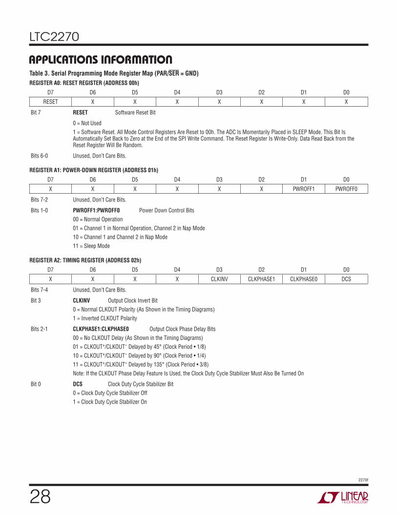
APPLICATIONS INFORMATIONTable 3. Serial Programming Mode Register Map (PAR/SER = GND)
REGISTER A0: RESET REGISTER (ADDRESS 00h)
D7 D6 D5 D4 D3 D2 D1 D0
RESET X X X X X X X
Bit 7 RESET Software Reset Bit
0 = Not Used
1 = Software Reset. All Mode Control Registers Are Reset to 00h. The ADC Is Momentarily Placed in SLEEP Mode. This Bit Is Automatically Set Back to Zero at the End of the SPI Write Command. The Reset Register Is Write-Only. Data Read Back from the Reset Register Will Be Random.
Bits 6-0 Unused, Don’t Care Bits.
REGISTER A1: POWER-DOWN REGISTER (ADDRESS 01h)
D7 D6 D5 D4 D3 D2 D1 D0
X X X X X X PWROFF1 PWROFF0
Bits 7-2 Unused, Don’t Care Bits.
Bits 1-0 PWROFF1:PWROFF0 Power Down Control Bits
00 = Normal Operation
01 = Channel 1 in Normal Operation, Channel 2 in Nap Mode
10 = Channel 1 and Channel 2 in Nap Mode
11 = Sleep Mode
REGISTER A2: TIMING REGISTER (ADDRESS 02h)
D7 D6 D5 D4 D3 D2 D1 D0
X X X X CLKINV CLKPHASE1 CLKPHASE0 DCS
Bits 7-4 Unused, Don’t Care Bits.
Bit 3 CLKINV Output Clock Invert Bit
0 = Normal CLKOUT Polarity (As Shown in the Timing Diagrams)
1 = Inverted CLKOUT Polarity
Bits 2-1 CLKPHASE1:CLKPHASE0 Output Clock Phase Delay Bits
00 = No CLKOUT Delay (As Shown in the Timing Diagrams)
01 = CLKOUT+/CLKOUT– Delayed by 45° (Clock Period • 1/8)
10 = CLKOUT+/CLKOUT– Delayed by 90° (Clock Period • 1/4)
11 = CLKOUT+/CLKOUT– Delayed by 135° (Clock Period • 3/8)
Note: If the CLKOUT Phase Delay Feature Is Used, the Clock Duty Cycle Stabilizer Must Also Be Turned On
Bit 0 DCS Clock Duty Cycle Stabilizer Bit
0 = Clock Duty Cycle Stabilizer Off
1 = Clock Duty Cycle Stabilizer On
292270f
LTC2270
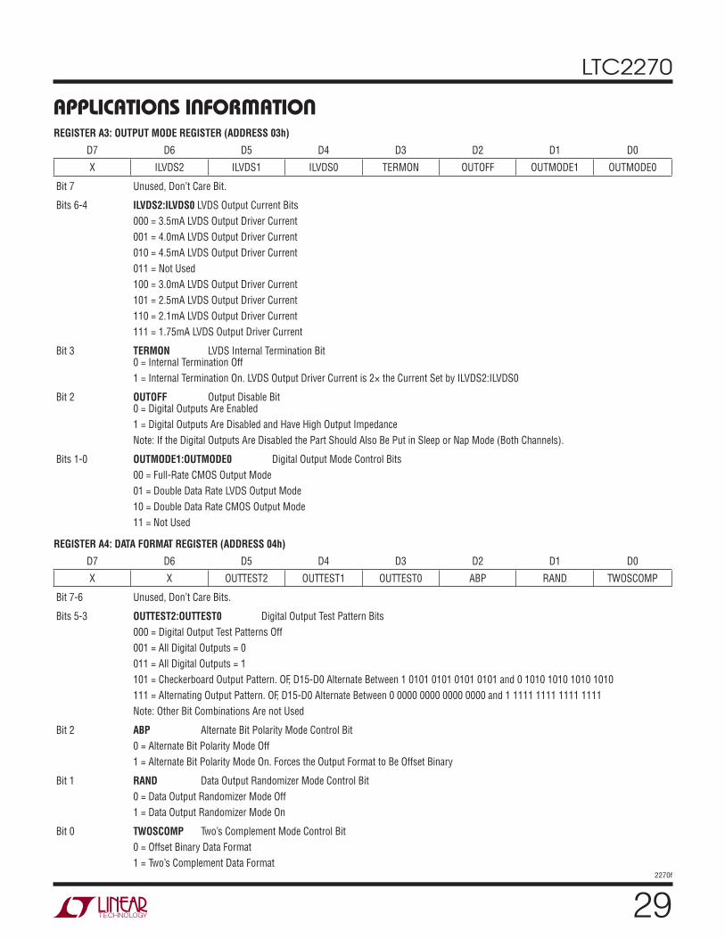
REGISTER A3: OUTPUT MODE REGISTER (ADDRESS 03h)
D7 D6 D5 D4 D3 D2 D1 D0
X ILVDS2 ILVDS1 ILVDS0 TERMON OUTOFF OUTMODE1 OUTMODE0
Bit 7 Unused, Don’t Care Bit.
Bits 6-4 ILVDS2:ILVDS0 LVDS Output Current Bits
000 = 3.5mA LVDS Output Driver Current
001 = 4.0mA LVDS Output Driver Current
010 = 4.5mA LVDS Output Driver Current
011 = Not Used
100 = 3.0mA LVDS Output Driver Current
101 = 2.5mA LVDS Output Driver Current
110 = 2.1mA LVDS Output Driver Current
111 = 1.75mA LVDS Output Driver Current
Bit 3 TERMON LVDS Internal Termination Bit0 = Internal Termination Off
1 = Internal Termination On. LVDS Output Driver Current is 2× the Current Set by ILVDS2:ILVDS0
Bit 2 OUTOFF Output Disable Bit0 = Digital Outputs Are Enabled
1 = Digital Outputs Are Disabled and Have High Output Impedance
Note: If the Digital Outputs Are Disabled the Part Should Also Be Put in Sleep or Nap Mode (Both Channels).
Bits 1-0 OUTMODE1:OUTMODE0 Digital Output Mode Control Bits
00 = Full-Rate CMOS Output Mode
01 = Double Data Rate LVDS Output Mode
10 = Double Data Rate CMOS Output Mode
11 = Not Used
REGISTER A4: DATA FORMAT REGISTER (ADDRESS 04h)
D7 D6 D5 D4 D3 D2 D1 D0
X X OUTTEST2 OUTTEST1 OUTTEST0 ABP RAND TWOSCOMP
Bit 7-6 Unused, Don’t Care Bits.
Bits 5-3 OUTTEST2:OUTTEST0 Digital Output Test Pattern Bits
000 = Digital Output Test Patterns Off
001 = All Digital Outputs = 0
011 = All Digital Outputs = 1
101 = Checkerboard Output Pattern. OF, D15-D0 Alternate Between 1 0101 0101 0101 0101 and 0 1010 1010 1010 1010
111 = Alternating Output Pattern. OF, D15-D0 Alternate Between 0 0000 0000 0000 0000 and 1 1111 1111 1111 1111
Note: Other Bit Combinations Are not Used
Bit 2 ABP Alternate Bit Polarity Mode Control Bit
0 = Alternate Bit Polarity Mode Off
1 = Alternate Bit Polarity Mode On. Forces the Output Format to Be Offset Binary
Bit 1 RAND Data Output Randomizer Mode Control Bit
0 = Data Output Randomizer Mode Off
1 = Data Output Randomizer Mode On
Bit 0 TWOSCOMP Two’s Complement Mode Control Bit
0 = Offset Binary Data Format
1 = Two’s Complement Data Format
APPLICATIONS INFORMATION
LTC2270
302270f
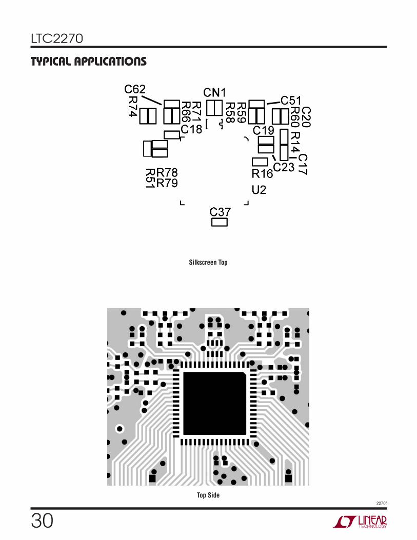
Silkscreen Top
TYPICAL APPLICATIONS
Top Side
312270f
LTC2270
TYPICAL APPLICATIONS
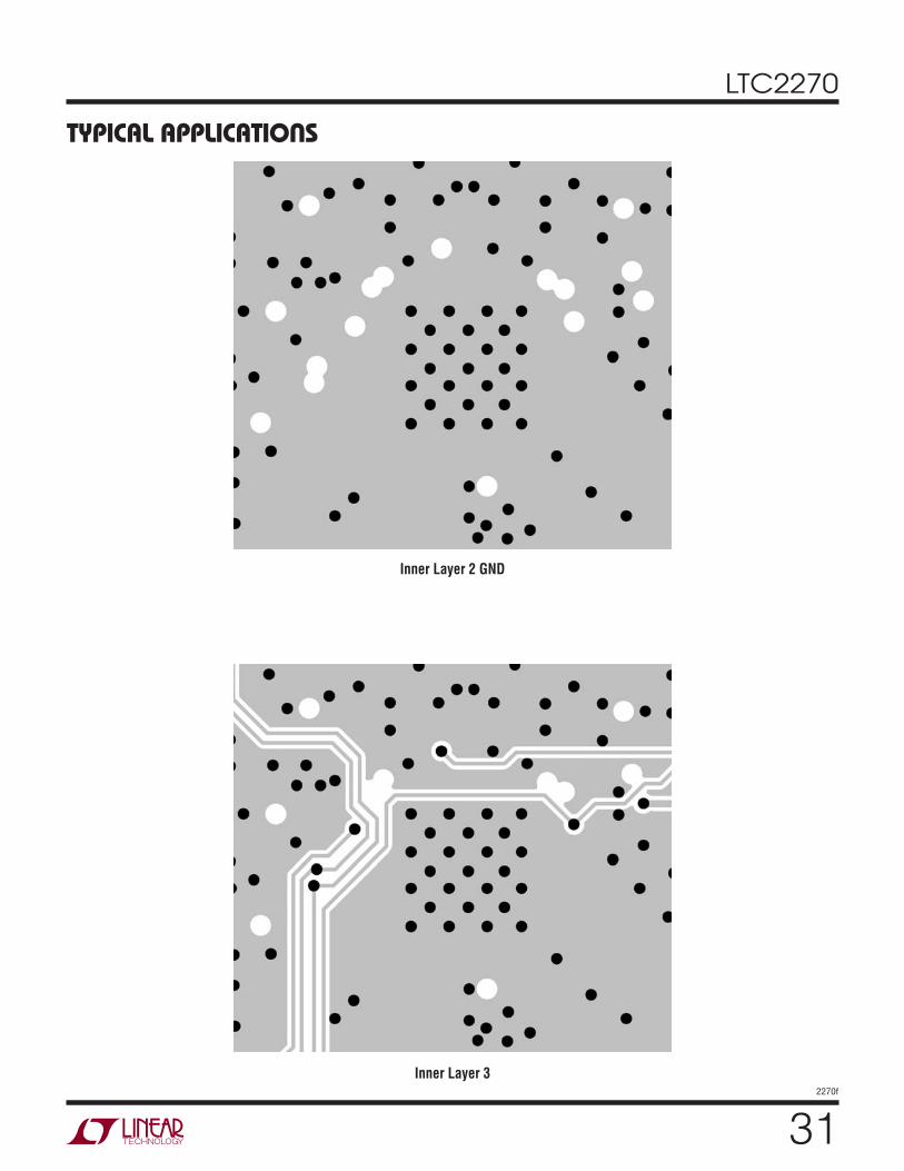
Inner Layer 2 GND
Inner Layer 3
LTC2270
322270f
TYPICAL APPLICATIONS
Inner Layer 4
Inner Layer 5 Power
332270f
LTC2270
TYPICAL APPLICATIONS
Bottom Side
LTC2270
342270f
48
47
46
45
44
43
42
41
40
39
38
37
36
35
34
33
D1_4_5+
D1_4_5–
D1_2_3+
D1_2_3–
D1_0_1+
D1_0_1–
OVDD
OGND
CLKOUT+
CLKOUT–
D2_14_15+
D2_14_15–
D2_12_13+
D2_12_13–
D2_10_11+
D2_10_11–
65PAD
64
63
62
61
60
59
58
57
56
55
54
53
52
51
50
49
VD
D
SEN
SE
VR
EF
SD
O
OF2
_1
+
OF2
_1
–
D1_14_15
+
D1_14_15
–
D1_12_13
+
D1_12_13
–
D1_10_11
+
D1_10_11
–
D1_8_9
+
D1_8_9
–
D1_6_7
+
D1_6_7
–
17
18
19
20
21
22
23
24
25
26
27
28
29
30
31
32
VD
D
EN
C+
EN
C–
CS
SC
K
SD
I
D2_0_1
–
D2_0_1
+
D2_2_3
–
D2_2_3
+
D2_4_5
–
D2_4_5
+
D2_6_7
–
D2_6_7
+
D2_8_9
–
D2_8_9
+
1
2
3
4
5
6
7
8
9
10
11
12
13
14
15
16
C190.1μF
SDO
VDD
VDD
VCM1
GND
AIN1+
AIN1–
GND
REFH
REFL
REFH
REFL
PAR/SER
AIN2+
AIN2–
GND
VCM2
VDD
C201μF
C180.1μF
VDD
PAR/SER
C171μF
C232.2μF
C370.1μF
DIGITALOUTPUTS
DIGITALOUTPUTS
OVDD
SPI BUS
C671μF
C780.1μF
C790.1μF
R51100Ω
LTC2270
ENCODECLOCK
CN1
AIN2+
AIN2–
AIN1+
AIN1–
C151μF
C211μF
+
+–
––
–+
+
SENSE
2270 TA03
TYPICAL APPLICATIONSLTC2270 Schematic
352270f
LTC2270
PACKAGE DESCRIPTION
Information furnished by Linear Technology Corporation is believed to be accurate and reliable. However, no responsibility is assumed for its use. Linear Technology Corporation makes no representa-tion that the interconnection of its circuits as described herein will not infringe on existing patent rights.
9 .00 ±0.10(4 SIDES)
NOTE:1. DRAWING CONFORMS TO JEDEC PACKAGE OUTLINE MO-220 VARIATION WNJR-52. ALL DIMENSIONS ARE IN MILLIMETERS3. DIMENSIONS OF EXPOSED PAD ON BOTTOM OF PACKAGE DO NOT INCLUDE MOLD FLASH. MOLD FLASH, IF PRESENT, SHALL NOT EXCEED 0.20mm ON ANY SIDE, IF PRESENT4. EXPOSED PAD SHALL BE SOLDER PLATED5. SHADED AREA IS ONLY A REFERENCE FOR PIN 1 LOCATION ON THE TOP AND BOTTOM OF PACKAGE 6. DRAWING NOT TO SCALE
PIN 1 TOP MARK(SEE NOTE 5)
0.40 ±0.10
6463
12
BOTTOM VIEW—EXPOSED PAD
7.15 ±0.10
7.15 ±0.10
7.50 REF(4-SIDES)
0.75 ±0.05R = 0.10
TYP
R = 0.115TYP
0.25 ±0.05
0.50 BSC
0.200 REF
0.00 – 0.05
(UP64) QFN 0406 REV C
RECOMMENDED SOLDER PAD PITCH AND DIMENSIONSAPPLY SOLDER MASK TO AREAS THAT ARE NOT SOLDERED
0.70 ±0.05
7.50 REF(4 SIDES)
7.15 ±0.05
7.15 ±0.05
8.10 ±0.05 9.50 ±0.05
0.25 ±0.050.50 BSC
PACKAGE OUTLINE
PIN 1CHAMFER
C = 0.35
UP Package64-Lead Plastic QFN (9mm 9mm)
(Reference LTC DWG # 05-08-1705 Rev C)
LTC2270
362270f
Linear Technology Corporation1630 McCarthy Blvd., Milpitas, CA 95035-7417 (408) 432-1900 ● FAX: (408) 434-0507 ● www.linear.com © LINEAR TECHNOLOGY CORPORATION 2012
LT 0812 • PRINTED IN USA
RELATED PARTSPART NUMBER DESCRIPTION COMMENTS
ADCs
LTC2160 16-Bit 25Msps 1.8V ADC, Ultralow Power 45mW, 77dB SNR, 90dB SFDR, DDR LVDS/DDR CMOS/CMOS Outputs, 7mm × 7mm QFN-48
LTC2180 16-Bit 25Msps 1.8V Dual ADC, Ultralow Power 39mW/Ch, 77dB SNR, 90dB SFDR, DDR LVDS/DDR CMOS/CMOS Outputs, 9mm × 9mm QFN-64
LTC2188 16-Bit 20Msps 1.8V Dual ADC, Ultralow Power 38mW/Ch, 77dB SNR, 90dB SFDR, DDR LVDS/DDR CMOS/CMOS Outputs, 9mm × 9mm QFN-64
LTC2190 16-Bit 25Msps 1.8V Dual ADC, Ultralow Power 52mW/Ch, 77dB SNR, 90dB SFDR, Serial LVDS Outputs, 7mm × 8mm QFN-52
LTC2202/LTC2203 16-Bit 10Msps/25Msps 3.3V ADCs 140mW/220mW, 81.6dB SNR, 100dB SFDR, CMOS Outputs, 7mm × 7mm QFN-48
PLLs
LTC6946-x Ultralow Noise and Spurious Integer-N Synthesizer with Integrated VCO
3.7MHz to 5.7GHz, –226dBc/Hz Normalized In-Band Phase Noise Floor –157dBc/Hz Wideband Output Phase Noise Floor
LTC6945 Ultralow Noise and Spurious 0.35GHz to 6GHz Integer-N Synthesizer
3.5GHz to 6GHz, –226dBc/Hz Normalized In-Band Phase Noise Floor –157dBc/Hz Wideband Output Phase Noise Floor
Signal Chain Receivers
LTM9002 14-Bit, Dual Channel IF/Baseband μModule Receiver
Dual ADC, Dual Amplifiers, Anti-Alias Filters and a Dual Trim DAC in 15mm × 11.25mm LGA
LTM9004 14-Bit, Direct Conversion μModule Receiver I/Q Demodulator, Baseband Amplifiers, Lowpass Filters Up to 20MHz, Dual 14-Bit 125Msps ADC in 22mm × 15mm LGA
RF Mixers/Demodulators
LTC5569 300MHz to 4GHz Dual Active Downconverting Mixer
High IIP3: 26.8dBm, 2dB Conversion Gain, Low Power: 3.3V/600mW, Integrated RF Transformer for compact Footprint
LTC5584 30MHz to 1.4GHz Wideband I/Q Demodulator I/Q Demodulation Bandwidth >530MHz, 31dBm IIP3, IIP2 Adjustable to >80dBm, DC Offset Adjustable to Zero, 45dB Image Rejection
LTC5585 700MHz to 3GHz Wideband I/Q Demodulator I/Q Demodulation Bandwidth >530MHz, 25.7dBm IIP3, IIP2 Adjustable to >80dBm, DC Offset Adjustable to Zero, 43dB Image Rejection
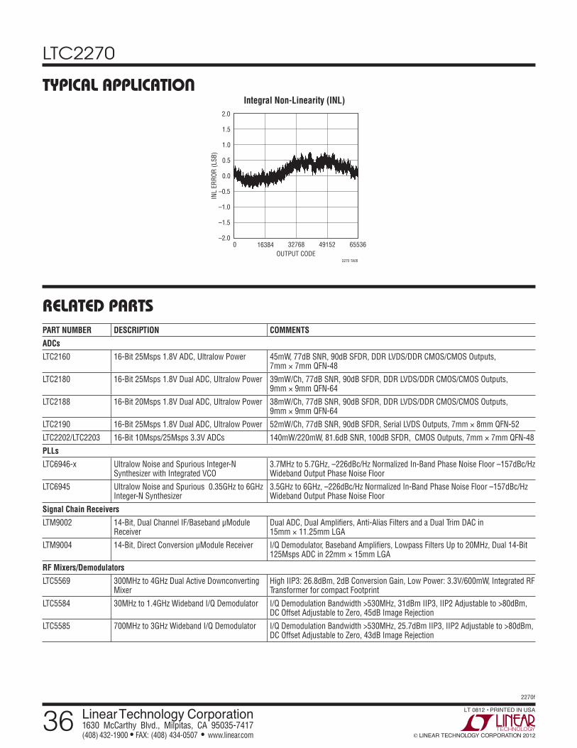
Integral Non-Linearity (INL)
OUTPUT CODE0
–2.0
–1.5
–1.0IN
L ER
ROR
(LSB
)
–0.5
0.5
0.0
1.0
1.5
2.0
16384 32768 49152 65536
2270 TA05
TYPICAL APPLICATION