Impact of Technology Scaling on Low Noise Front End … · Impact of Technology Scaling on Low...
57
Impact of Technology Scaling on Impact of Technology Scaling on Low Noise Front End Circuits Low Noise Front End Circuits Paul O’Connor, Brookhaven National Laboratory Snowmass 2001 July 9 2001
Transcript of Impact of Technology Scaling on Low Noise Front End … · Impact of Technology Scaling on Low...
Impact of Technology Scaling on Impact of Technology Scaling on Low Noise Front End CircuitsLow Noise Front End Circuits
Paul O’Connor, Brookhaven National Laboratory
Snowmass 2001
July 9 2001
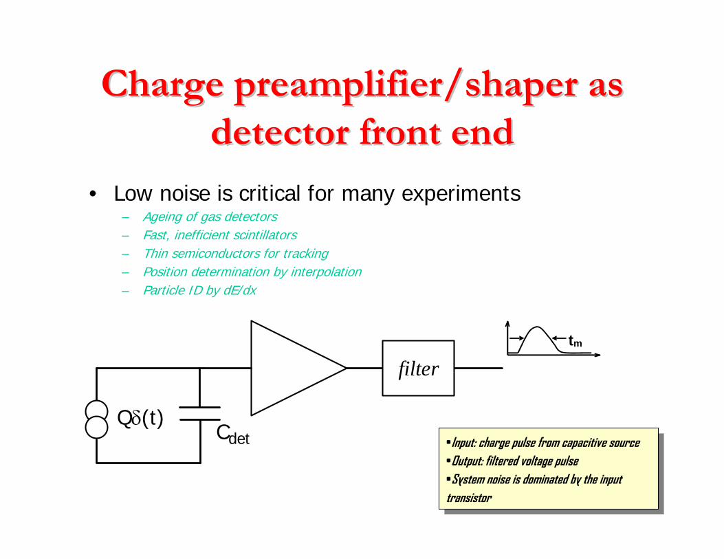
Charge preamplifier/shaper as Charge preamplifier/shaper as detector front enddetector front end
• Low noise is critical for many experiments– Ageing of gas detectors– Fast, inefficient scintillators– Thin semiconductors for tracking– Position determination by interpolation– Particle ID by dE/dx
•Input: charge pulse from capacitive source•Output: filtered voltage pulse•System noise is dominated by the input transistor
•Input: charge pulse from capacitive source•Output: filtered voltage pulse•System noise is dominated by the input transistor
Qδ(t)Cdet
filtertm
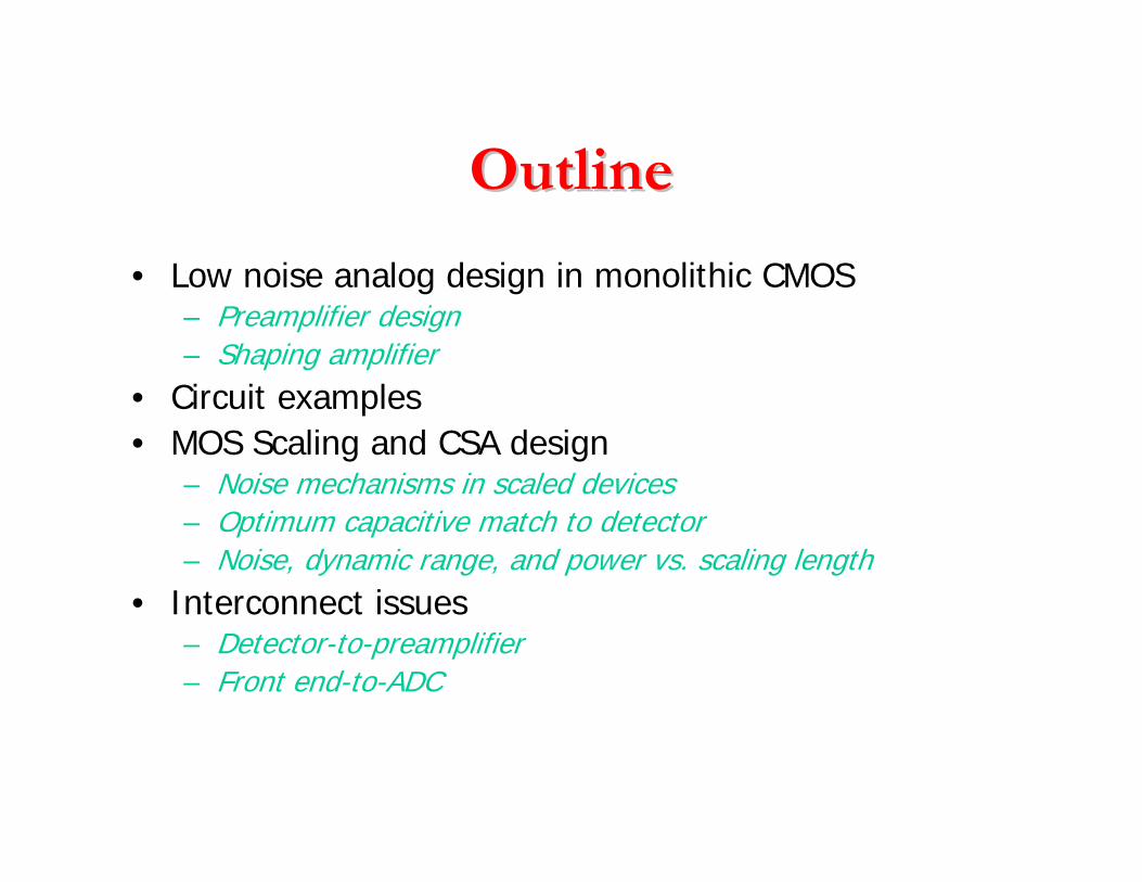
OutlineOutline
• Low noise analog design in monolithic CMOS– Preamplifier design– Shaping amplifier
• Circuit examples• MOS Scaling and CSA design
– Noise mechanisms in scaled devices– Optimum capacitive match to detector– Noise, dynamic range, and power vs. scaling length
• Interconnect issues– Detector-to-preamplifier– Front end-to-ADC

Low Noise Analog DesignLow Noise Analog Design
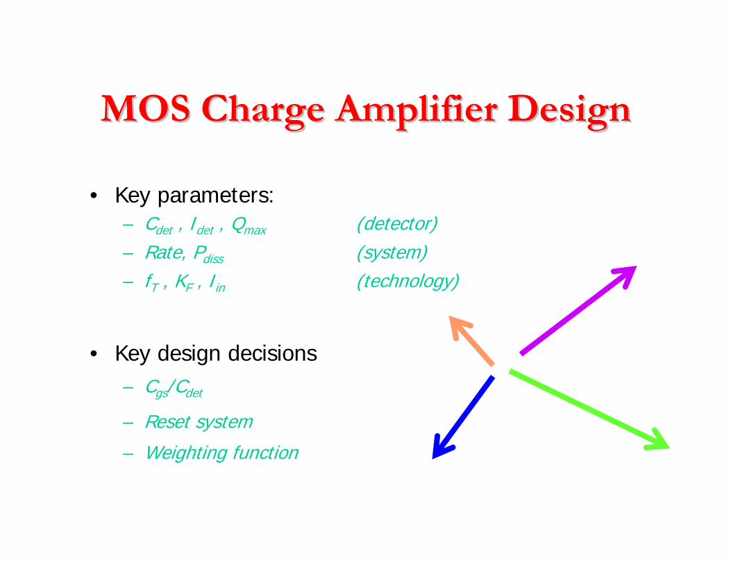
MOS Charge Amplifier DesignMOS Charge Amplifier Design
• Key parameters:– Cdet , Idet , Qmax (detector)– Rate, Pdiss (system)– fT , KF , Iin (technology)
• Key design decisions– Cgs/Cdet
– Reset system
– Weighting function
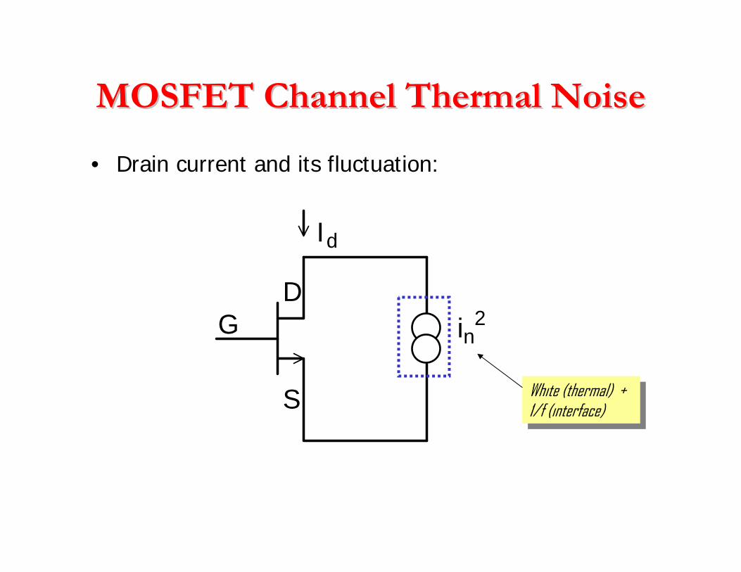
MOSFET Channel Thermal NoiseMOSFET Channel Thermal Noise
• Drain current and its fluctuation:
in2
D
S
G
Id
White (thermal) + 1/f (interface)
White (thermal) + 1/f (interface)
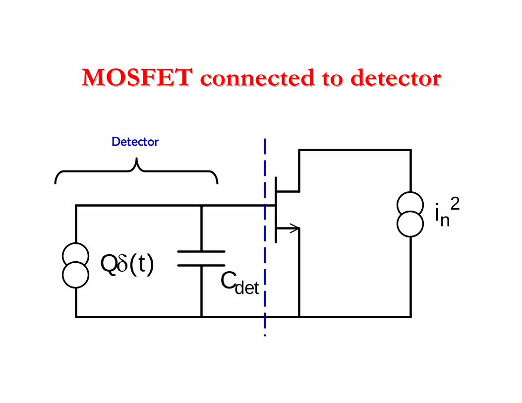
MOSFET connected to detectorMOSFET connected to detector
Cdet
in2
Qδ(t)
Detector
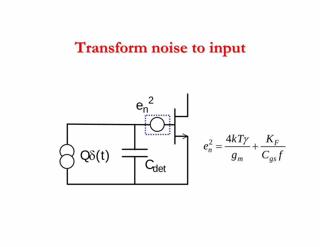
Transform noise to inputTransform noise to input
Cdet
en2
Qδ(t) fCK
gkTe
gs
F
mn +=
γ42
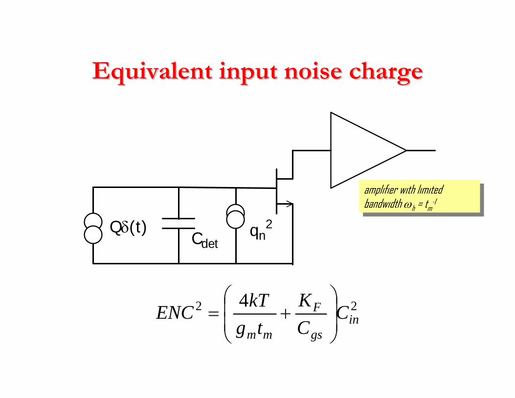
Equivalent input noise chargeEquivalent input noise charge
Cdetqn
2Qδ(t)
amplifier with limitedbandwidth ωh = tm
-1
amplifier with limitedbandwidth ωh = tm
-1
22 4in
gs
F
mmC
CK
tgkTENC ⎟
⎟⎠
⎞⎜⎜⎝
⎛+=
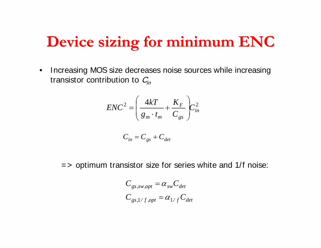
• Increasing MOS size decreases noise sources while increasing transistor contribution to Cin
Device sizing for minimum ENCDevice sizing for minimum ENC
detgsin CCC +=
22 4in
gs
F
mmC
CK
tgkTENC ⎟
⎟⎠
⎞⎜⎜⎝
⎛+
⋅=
detf/opt,f/,gs
detswopt,sw,gs
CC
CC
11 α
α
=
=
=> optimum transistor size for series white and 1/f noise:
Optimized ENCOptimized ENC
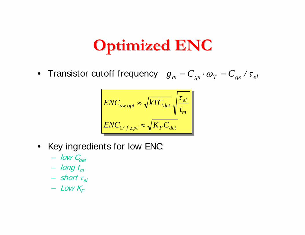
• Transistor cutoff frequency
• Key ingredients for low ENC:– low Cdet
– long tm– short τel
– Low KF
elgsTgsm /CCg τω =⋅=
detFopt,f/
m
eldetopt,sw
CKENC
tkTCENC
≈
≈
1
τ
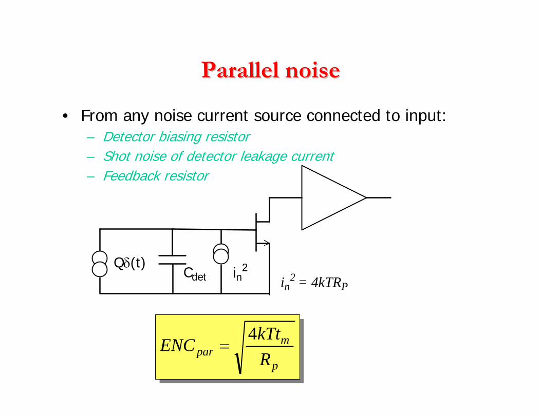
Parallel noiseParallel noise
• From any noise current source connected to input:– Detector biasing resistor– Shot noise of detector leakage current– Feedback resistor
p
mpar R
kTtENC 4=
CdetQδ(t)
in2 = 4kTRPin
2
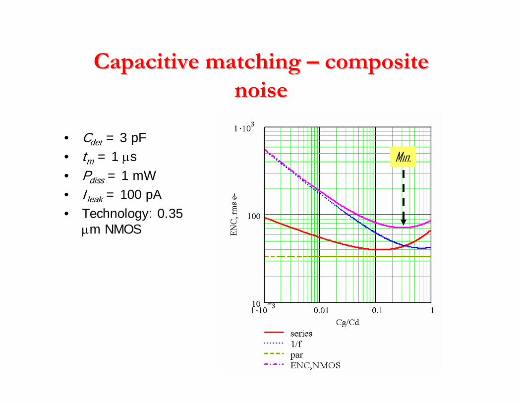
Capacitive matching Capacitive matching –– composite composite noisenoise
• Cdet = 3 pF• tm = 1 µs• Pdiss = 1 mW• Ileak = 100 pA• Technology: 0.35
µm NMOS
Min.
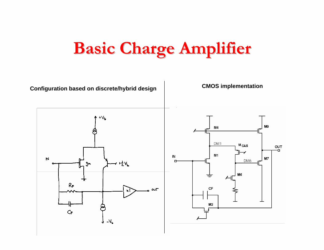
Basic Charge AmplifierBasic Charge Amplifier
Configuration based on discrete/hybrid design CMOS implementation
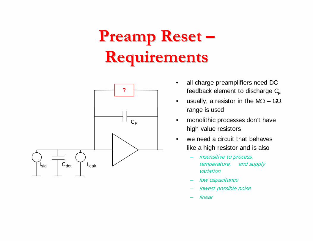
Preamp Reset Preamp Reset ––RequirementsRequirements
• all charge preamplifiers need DC feedback element to discharge CF
• usually, a resistor in the MΩ – GΩrange is used
• monolithic processes don’t have high value resistors
• we need a circuit that behaves like a high resistor and is also
– insensitive to process, temperature, and supply variation
– low capacitance– lowest possible noise– linear
Cdet
CF
?
Isig Ileak
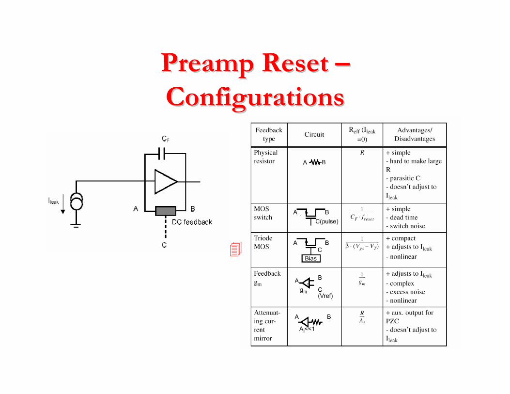
Preamp Reset Preamp Reset ––ConfigurationsConfigurations
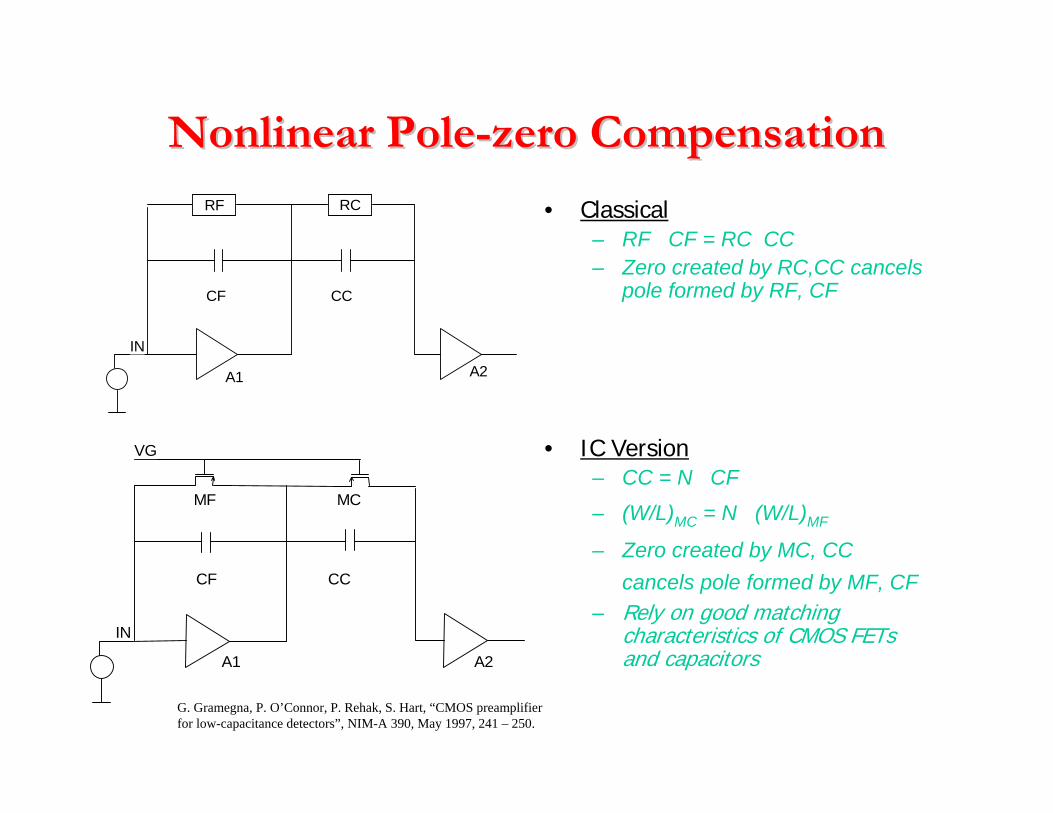
Nonlinear PoleNonlinear Pole--zero Compensationzero Compensation
• Classical– RF · CF = RC ·CC– Zero created by RC,CC cancels
pole formed by RF, CF
• IC Version– CC = N · CF
– (W/L)MC = N · (W/L)MF
– Zero created by MC, CC cancels pole formed by MF, CF
– Rely on good matching characteristics of CMOS FETsand capacitors
IN
CCCF
A1 A2
RF RC
VG
IN
CC
MC
CF
MF
A1 A2
G. Gramegna, P. O’Connor, P. Rehak, S. Hart, “CMOS preamplifier for low-capacitance detectors”, NIM-A 390, May 1997, 241 – 250.
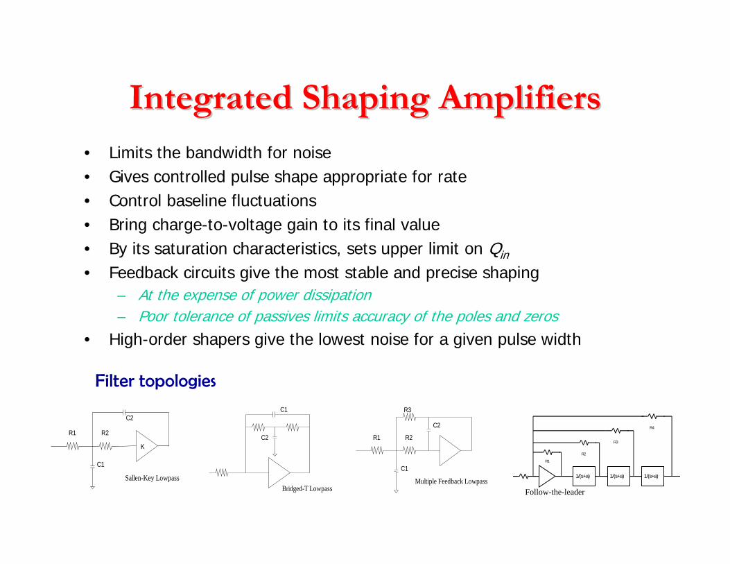
Integrated Shaping AmplifiersIntegrated Shaping Amplifiers• Limits the bandwidth for noise• Gives controlled pulse shape appropriate for rate• Control baseline fluctuations• Bring charge-to-voltage gain to its final value• By its saturation characteristics, sets upper limit on Qin
• Feedback circuits give the most stable and precise shaping – At the expense of power dissipation– Poor tolerance of passives limits accuracy of the poles and zeros
• High-order shapers give the lowest noise for a given pulse width
Sallen-Key Lowpass
R1 R2
C1
C2
K
Bridged-T Lowpass
C1
C2
Multiple Feedback Lowpass
R3
R1 R2
C1
C2
1/(s+a) 1/(s+a)1/(s+a)
R1
R2
R3
R4
Follow-the-leader
Filter topologies
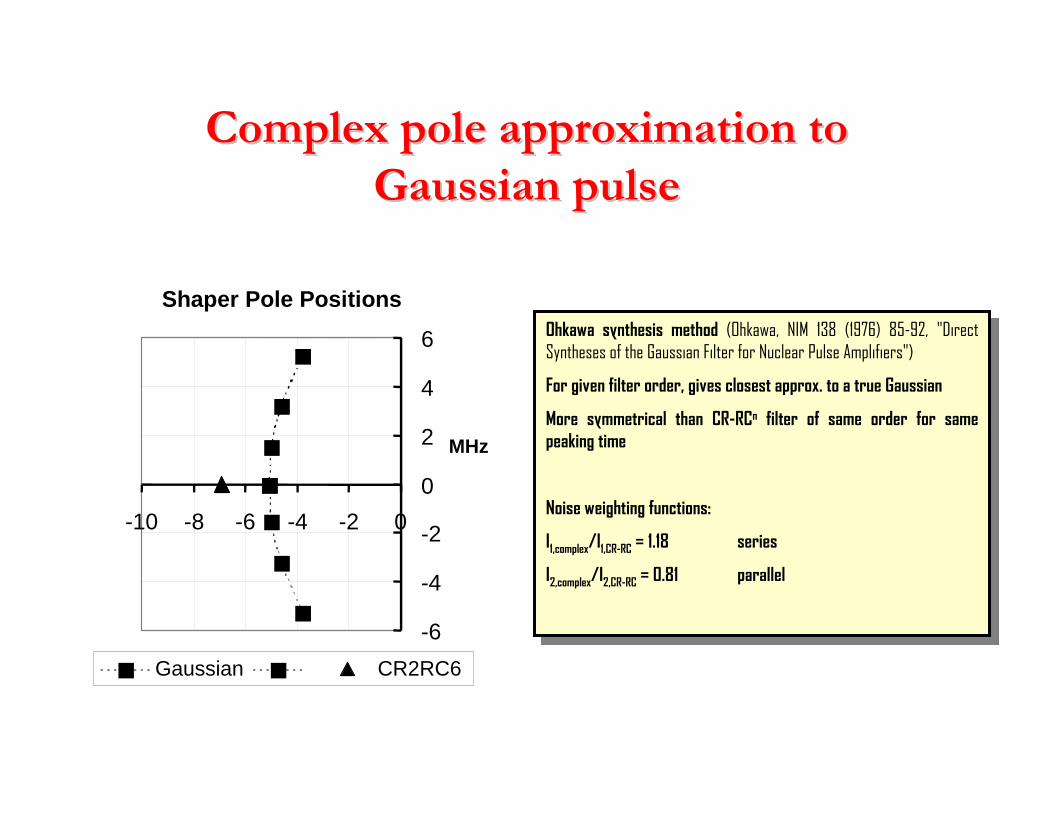
Complex pole approximation to Complex pole approximation to Gaussian pulse Gaussian pulse
Shaper Pole Positions
-6
-4
-2
0
2
4
6
-10 -8 -6 -4 -2 0
MHz
Gaussian CR2RC6
Ohkawa synthesis method (Ohkawa, NIM 138 (1976) 85-92, "Direct Syntheses of the Gaussian Filter for Nuclear Pulse Amplifiers")
For given filter order, gives closest approx. to a true Gaussian
More symmetrical than CR-RCn filter of same order for same peaking time
Noise weighting functions:
I1,complex/I1,CR-RC = 1.18 series
I2,complex/I2,CR-RC = 0.81 parallel
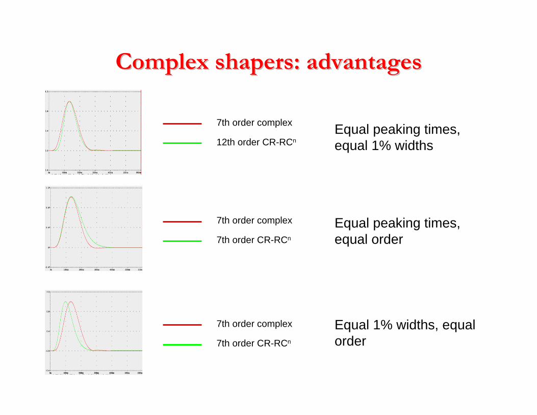
Complex shapers: advantagesComplex shapers: advantages
7th order complex
12th order CR-RCn
Equal peaking times, equal order
7th order complex
7th order CR-RCn
Equal 1% widths, equal order
7th order complex
7th order CR-RCn
Equal peaking times, equal 1% widths
ExamplesExamples
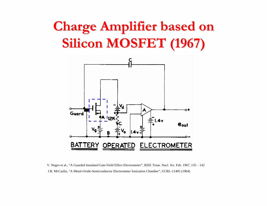
Charge Amplifier based on Charge Amplifier based on Silicon MOSFET (1967)Silicon MOSFET (1967)
V. Negro et al., “A Guarded Insulated Gate Field Effect Electrometer”, IEEE Trnas. Nucl. Sci. Feb. 1967, 135 – 142
J.B. McCaslin, “A Metal-Oxide-Semiconductor Electrometer Ionization Chamber”, UCRL-11405 (1964)
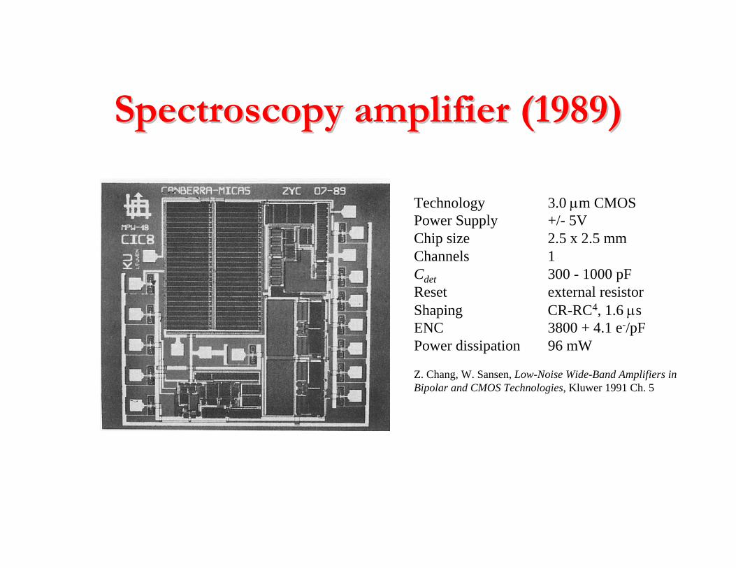
Spectroscopy amplifier (1989)Spectroscopy amplifier (1989)
Technology 3.0 µm CMOSPower Supply +/- 5VChip size 2.5 x 2.5 mmChannels 1Cdet 300 - 1000 pFReset external resistorShaping CR-RC4, 1.6 µsENC 3800 + 4.1 e-/pFPower dissipation 96 mW
Z. Chang, W. Sansen, Low-Noise Wide-Band Amplifiers in Bipolar and CMOS Technologies, Kluwer 1991 Ch. 5
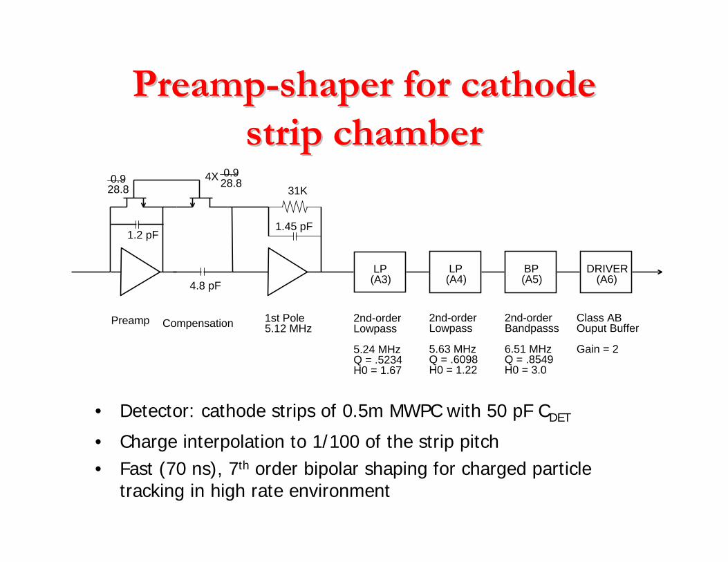
PreampPreamp--shaper for cathode shaper for cathode strip chamberstrip chamber
LP(A3)
Preamp Compensation 1st Pole5.12 MHz
2nd-orderLowpass
5.24 MHzQ = .5234H0 = 1.67
LP(A4)
2nd-orderLowpass
5.63 MHzQ = .6098H0 = 1.22
BP(A5)
2nd-orderBandpasss
6.51 MHzQ = .8549H0 = 3.0
DRIVER(A6)
Class ABOuput Buffer
Gain = 2
1.2 pF
4.8 pF
1.45 pF
31K0.9
28.80.9
28.84X
• Detector: cathode strips of 0.5m MWPC with 50 pF CDET
• Charge interpolation to 1/100 of the strip pitch• Fast (70 ns), 7th order bipolar shaping for charged particle
tracking in high rate environment
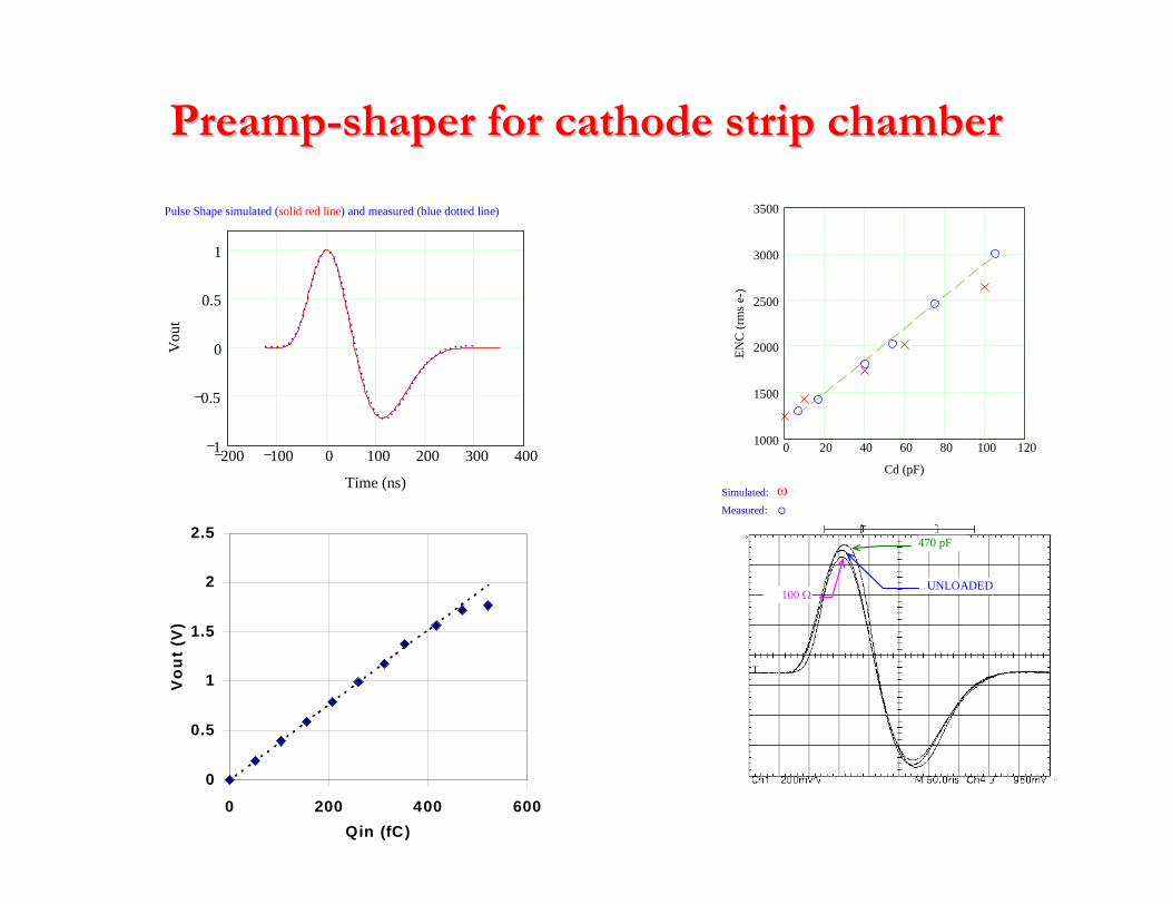
PreampPreamp--shaper for cathode strip chambershaper for cathode strip chamber
200 100 0 100 200 300 4001
0.5
0
0.5
1
Time (ns)
Vou
t
Pulse Shape simulated (solid red line) and measured (blue dotted line)
0
0.5
1
1.5
2
2.5
0 200 400 600Qin (fC)
Vo
ut
(V)
Simulated: ωMeasured: o
0 20 40 60 80 100 1201000
1500
2000
2500
3000
3500
Cd (pF)
ENC
(rm
s e-)
470 pF
100 ΩUNLOADED
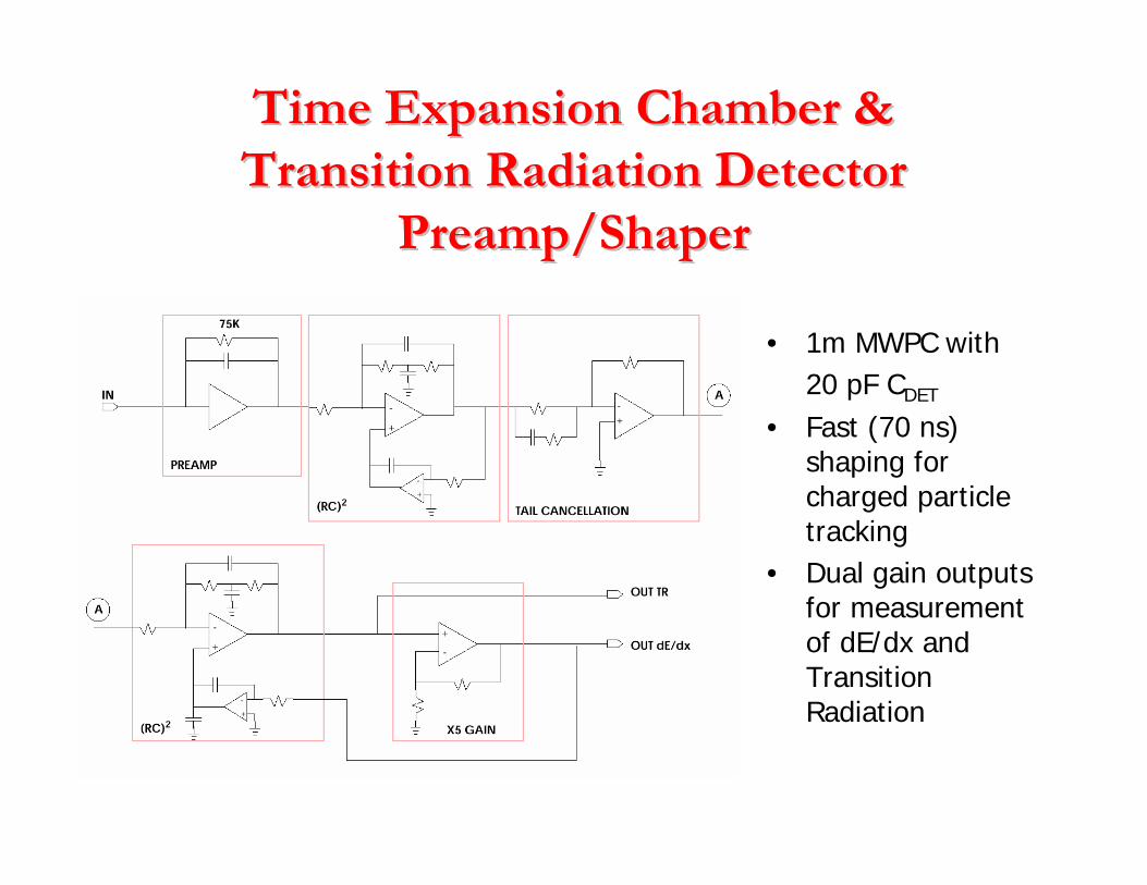
Time Expansion Chamber & Time Expansion Chamber & Transition Radiation Detector Transition Radiation Detector
Preamp/ShaperPreamp/Shaper
• 1m MWPC with 20 pF CDET
• Fast (70 ns) shaping for charged particle tracking
• Dual gain outputs for measurement of dE/dx and Transition Radiation
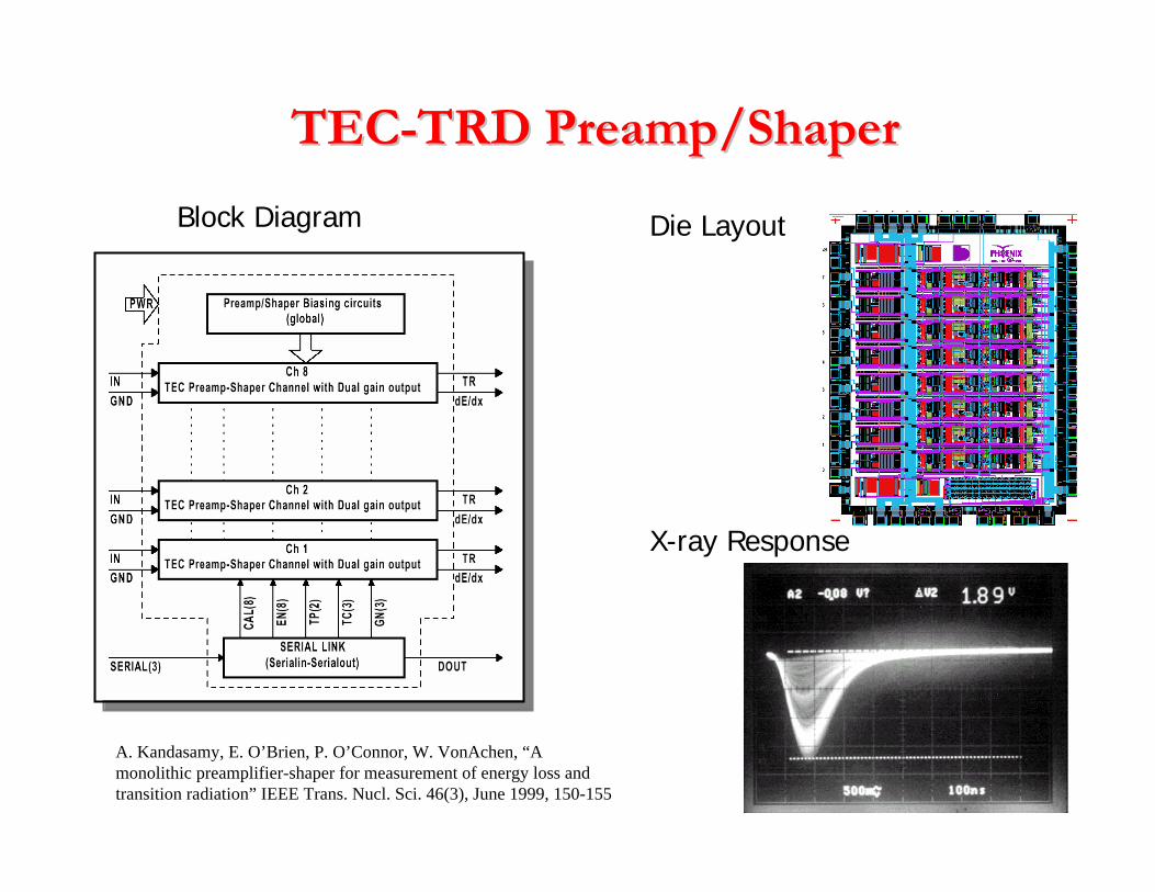
TECTEC--TRD Preamp/ShaperTRD Preamp/Shaper
Block Diagram Die Layout
X-ray Response
A. Kandasamy, E. O’Brien, P. O’Connor, W. VonAchen, “A monolithic preamplifier-shaper for measurement of energy loss and transition radiation” IEEE Trans. Nucl. Sci. 46(3), June 1999, 150-155
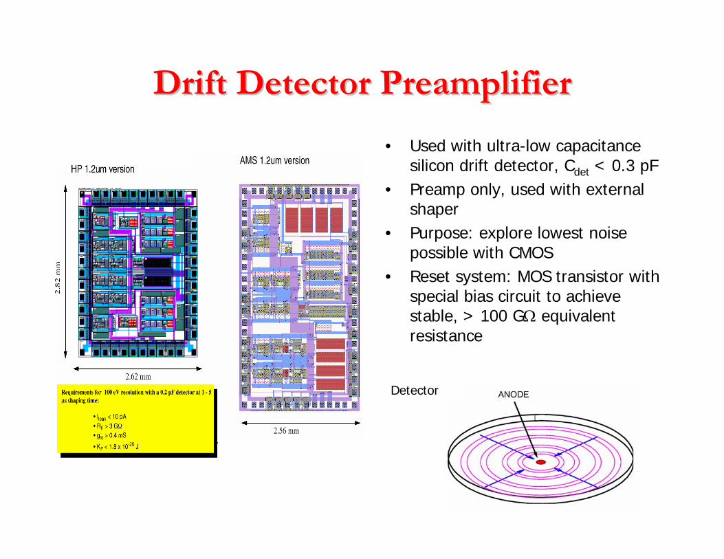
Drift Detector PreamplifierDrift Detector Preamplifier
• Used with ultra-low capacitance silicon drift detector, Cdet < 0.3 pF
• Preamp only, used with external shaper
• Purpose: explore lowest noise possible with CMOS
• Reset system: MOS transistor with special bias circuit to achieve stable, > 100 GΩ equivalent resistance
Detector
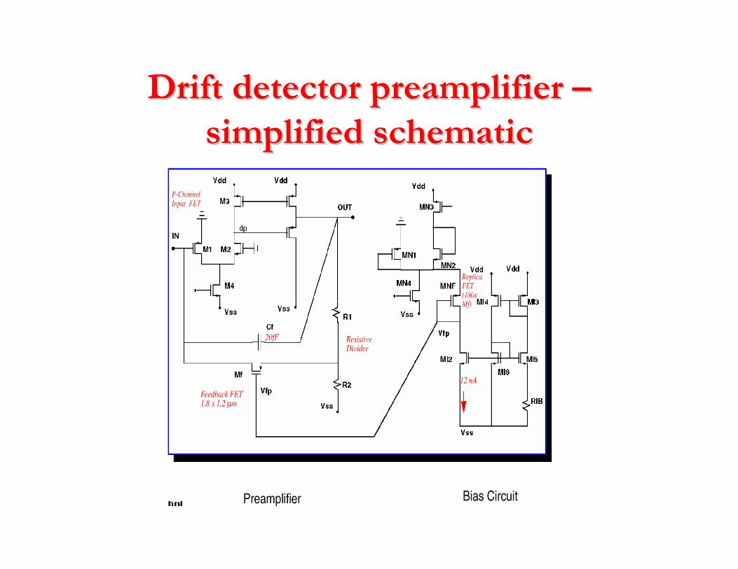
Drift detector preamplifier Drift detector preamplifier ––simplified schematicsimplified schematic
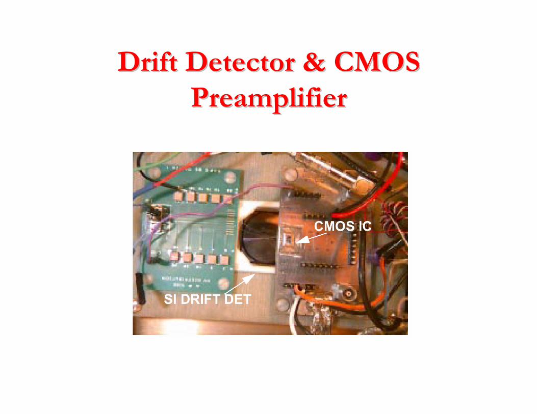
Drift Detector & CMOS Drift Detector & CMOS PreamplifierPreamplifier
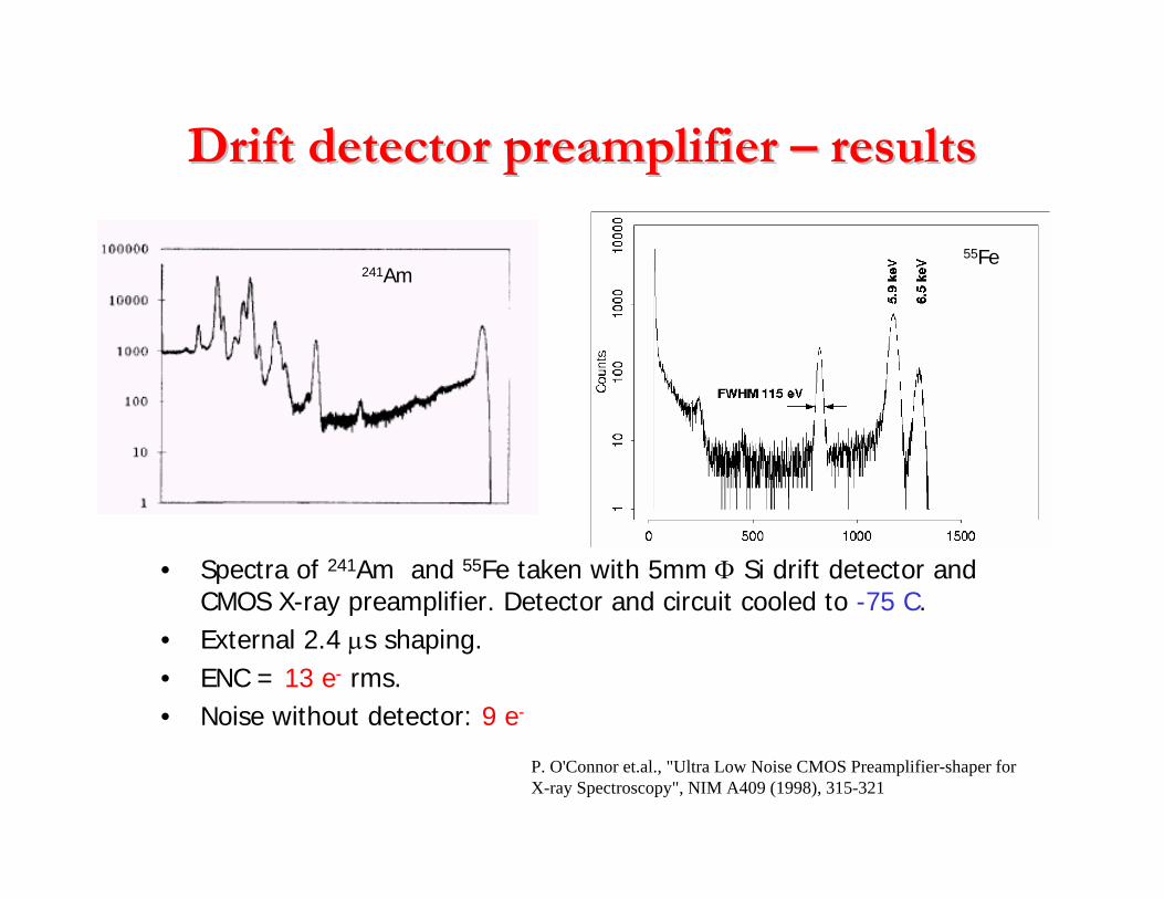
Drift detector preamplifier Drift detector preamplifier –– resultsresults
• Spectra of 241Am and 55Fe taken with 5mm Φ Si drift detector and CMOS X-ray preamplifier. Detector and circuit cooled to -75 C.
• External 2.4 µs shaping.• ENC = 13 e- rms.• Noise without detector: 9 e-
P. O'Connor et.al., "Ultra Low Noise CMOS Preamplifier-shaper for X-ray Spectroscopy", NIM A409 (1998), 315-321
241Am55Fe
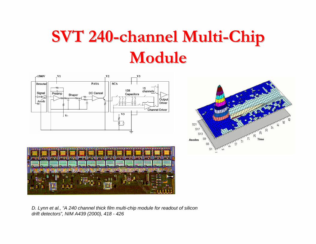
D. Lynn et al., “A 240 channel thick film multi-chip module for readout of silicon drift detectors”, NIM A439 (2000), 418 - 426
SVT 240SVT 240--channel Multichannel Multi--Chip Chip ModuleModule
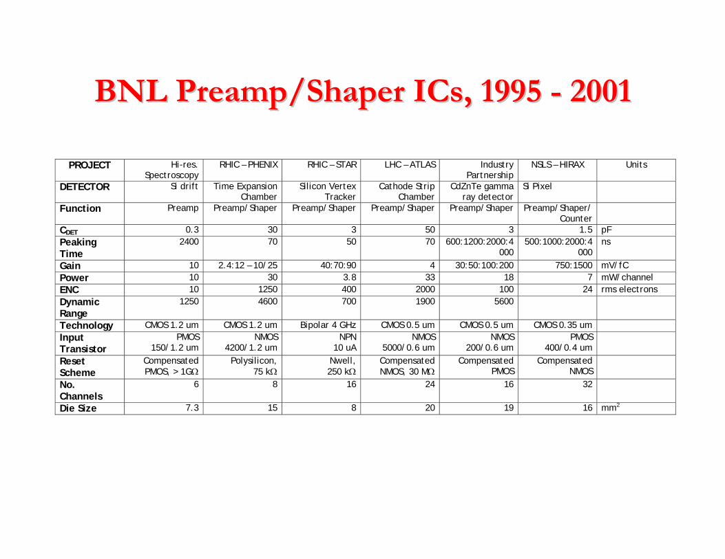
PROJECT Hi-res. Spectroscopy
RHIC – PHENIX RHIC – STAR LHC – ATLAS Industry Partnership
NSLS – HIRAX Units
DETECTOR Si drift Time Expansion Chamber
Silicon Vertex Tracker
Cathode Strip Chamber
CdZnTe gamma ray detector
Si Pixel
Function Preamp Preamp/Shaper Preamp/Shaper Preamp/Shaper Preamp/Shaper Preamp/Shaper/Counter
CDET 0.3 30 3 50 3 1.5 pF Peaking Time
2400 70 50 70 600:1200:2000:4000
500:1000:2000:4000
ns
Gain 10 2.4:12 – 10/25 40:70:90 4 30:50:100:200 750:1500 mV/fC Power 10 30 3.8 33 18 7 mW/channel ENC 10 1250 400 2000 100 24 rms electrons Dynamic Range
1250 4600 700 1900 5600
Technology CMOS 1.2 um CMOS 1.2 um Bipolar 4 GHz CMOS 0.5 um CMOS 0.5 um CMOS 0.35 um Input Transistor
PMOS 150/1.2 um
NMOS 4200/1.2 um
NPN 10 uA
NMOS 5000/0.6 um
NMOS 200/0.6 um
PMOS 400/0.4 um
Reset Scheme
Compensated PMOS, > 1GΩ
Polysilicon, 75 kΩ
Nwell, 250 kΩ
Compensated NMOS, 30 MΩ
Compensated PMOS
Compensated NMOS
No. Channels
6 8 16 24 16 32
Die Size 7.3 15 8 20 19 16 mm2
BNL Preamp/Shaper ICs, 1995 BNL Preamp/Shaper ICs, 1995 -- 20012001
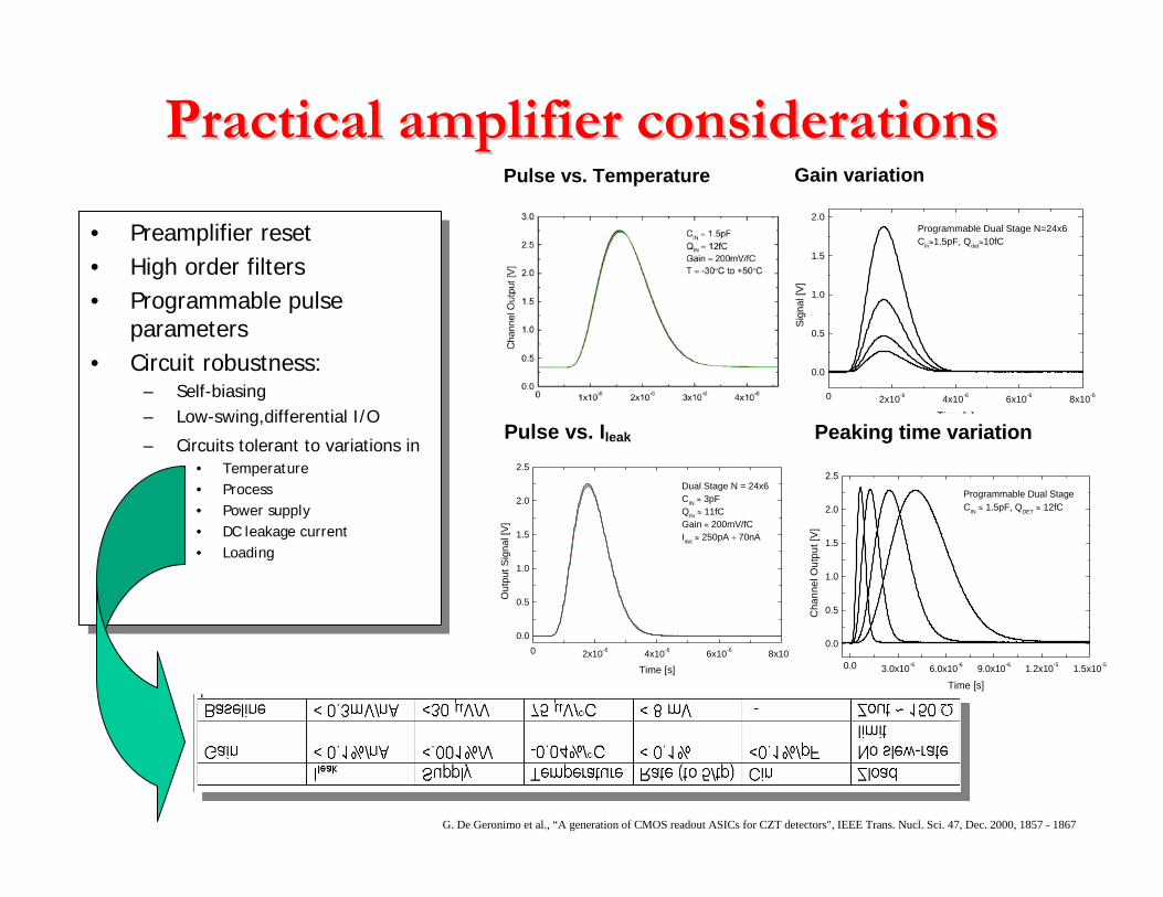
• Preamplifier reset• High order filters• Programmable pulse
parameters• Circuit robustness:
– Self-biasing– Low-swing,differential I/O
– Circuits tolerant to variations in• Temperature• Process • Power supply• DC leakage current• Loading
• Preamplifier reset• High order filters• Programmable pulse
parameters• Circuit robustness:
– Self-biasing– Low-swing,differential I/O
– Circuits tolerant to variations in• Temperature• Process • Power supply• DC leakage current• Loading
Practical amplifier considerationsPractical amplifier considerationsPulse vs. Temperature
0 2x10⁻⁶ 4x10⁻⁶ 6x10⁻⁶ 8x10⁻⁶
0.0
0.5
1.0
1.5
2.0Programmable Dual Stage N=24x6Cin≈1.5pF, Qdet≈10fC
Sig
nal [
V]
Time [s]
Gain variation
0 2x10⁻⁶ 4x10⁻⁶ 6x10⁻⁶ 8x10-
0.0
0.5
1.0
1.5
2.0
2.5
Dual Stage N = 24x6CIN ≈ 3pFQIN ≈ 11fCGain ≈ 200mV/fCIdet ≈ 250pA ÷ 70nA
Out
put S
igna
l [V
]
Time [s]
Pulse vs. Ileak
0.0 3.0x10⁻⁶ 6.0x10⁻⁶ 9.0x10⁻⁶ 1.2x10⁻⁵ 1.5x10⁻⁵
0.0
0.5
1.0
1.5
2.0
2.5
Programmable Dual StageCIN ≈ 1.5pF, QDET ≈ 12fC
Cha
nnel
Out
put [
V]
Time [s]
Peaking time variation
G. De Geronimo et al., “A generation of CMOS readout ASICs for CZT detectors", IEEE Trans. Nucl. Sci. 47, Dec. 2000, 1857 - 1867
MOS Scaling and Charge MOS Scaling and Charge Amplifier DesignAmplifier Design
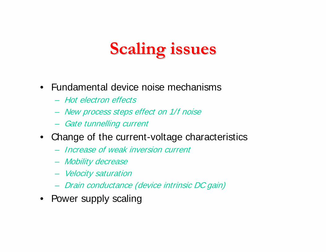
Scaling issuesScaling issues
• Fundamental device noise mechanisms– Hot electron effects– New process steps effect on 1/f noise– Gate tunnelling current
• Change of the current-voltage characteristics– Increase of weak inversion current– Mobility decrease– Velocity saturation– Drain conductance (device intrinsic DC gain)
• Power supply scaling
Series white noiseSeries white noise
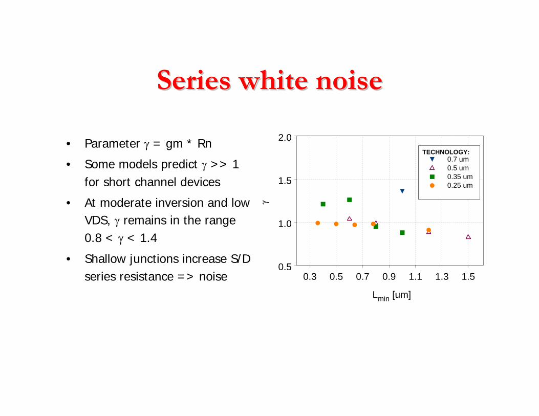
• Parameter γ = gm * Rn
• Some models predict γ >> 1 for short channel devices
• At moderate inversion and low VDS, γ remains in the range 0.8 < γ < 1.4
• Shallow junctions increase S/D series resistance => noise 0.3 0.5 0.7 0.9 1.1 1.3 1.5
Lmin [um]
0.5
1.0
1.5
2.0
γ
0.7 um0.5 um0.35 um0.25 um
TECHNOLOGY:
1/f noise in submicron CMOS1/f noise in submicron CMOS
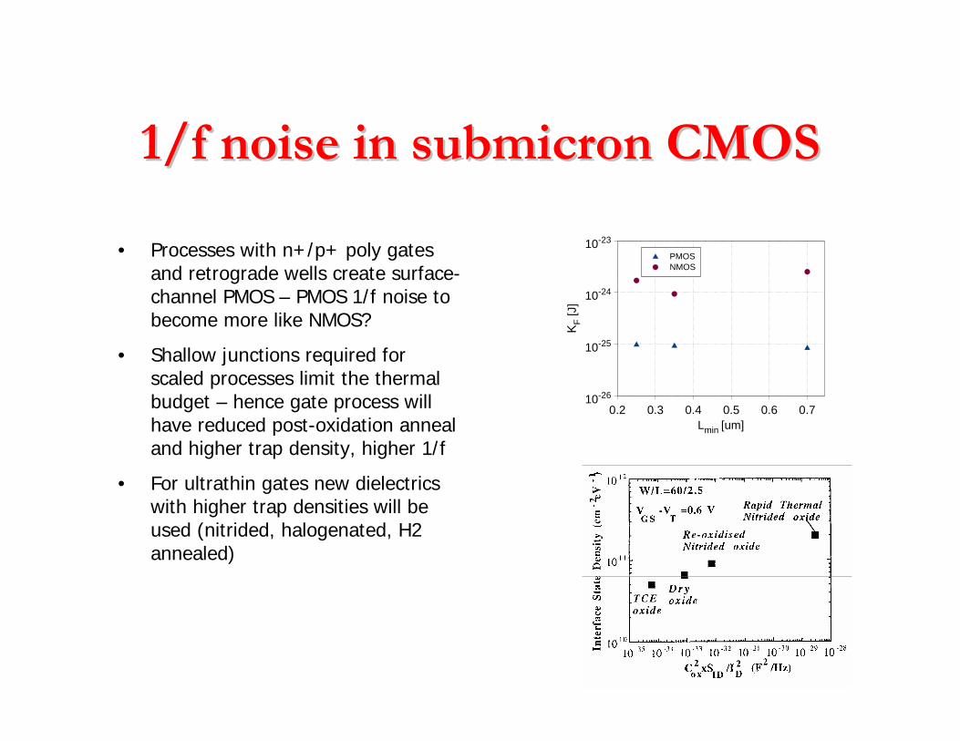
• Processes with n+/p+ poly gates and retrograde wells create surface-channel PMOS – PMOS 1/f noise to become more like NMOS?
• Shallow junctions required for scaled processes limit the thermal budget – hence gate process will have reduced post-oxidation anneal and higher trap density, higher 1/f
• For ultrathin gates new dielectrics with higher trap densities will be used (nitrided, halogenated, H2 annealed)
0.2 0.3 0.4 0.5 0.6 0.7Lmin [um]
10-26
10-25
10-24
10-23
KF
[J]
PMOSNMOS
1/f noise and hot carrier stress1/f noise and hot carrier stress
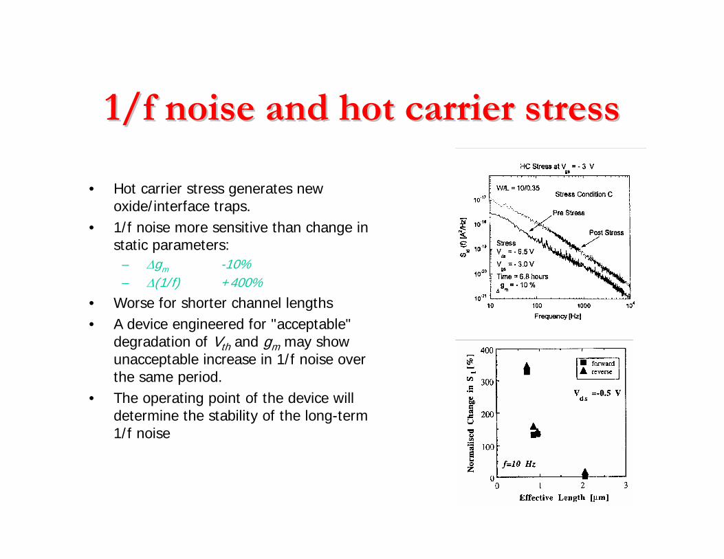
• Hot carrier stress generates new oxide/interface traps.
• 1/f noise more sensitive than change in static parameters:
– ∆gm -10%– ∆(1/f) +400%
• Worse for shorter channel lengths• A device engineered for "acceptable"
degradation of Vth and gm may show unacceptable increase in 1/f noise over the same period.
• The operating point of the device will determine the stability of the long-term 1/f noise
Gate tunneling currentGate tunneling current
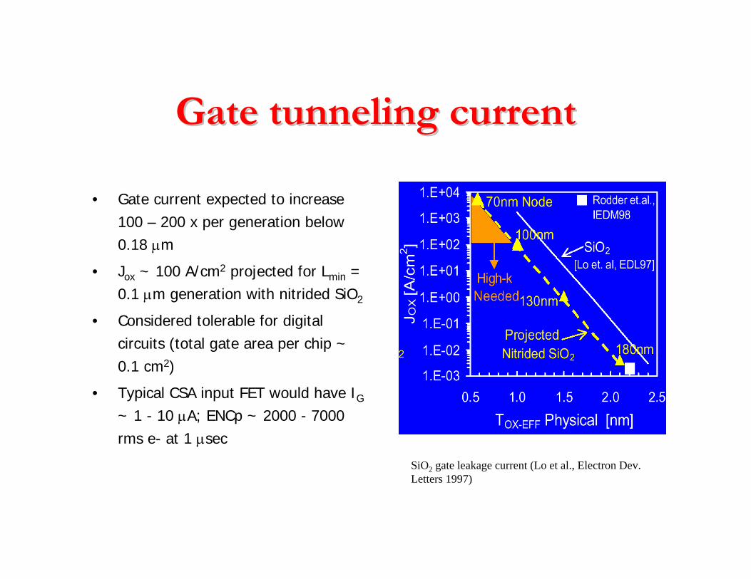
• Gate current expected to increase 100 – 200 x per generation below 0.18 µm
• Jox ~ 100 A/cm2 projected for Lmin = 0.1 µm generation with nitrided SiO2
• Considered tolerable for digital circuits (total gate area per chip ~ 0.1 cm2)
• Typical CSA input FET would have IG
~ 1 - 10 µA; ENCp ~ 2000 - 7000 rms e- at 1 µsec
SiO2 gate leakage current (Lo et al., Electron Dev. Letters 1997)
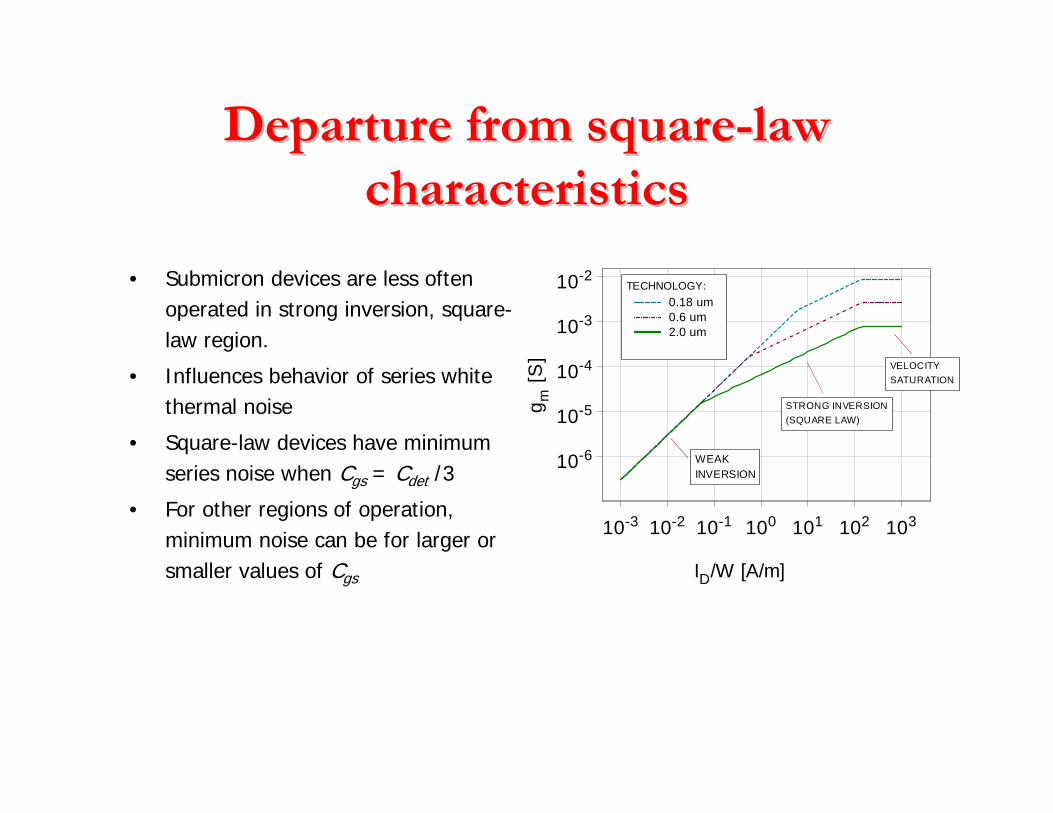
Departure from squareDeparture from square--law law characteristicscharacteristics
• Submicron devices are less often operated in strong inversion, square-law region.
• Influences behavior of series white thermal noise
• Square-law devices have minimum series noise when Cgs = Cdet /3
• For other regions of operation, minimum noise can be for larger or smaller values of Cgs
10-3 10-2 10-1 100 101 102 103
ID/W [A/m]
10-6
10-5
10-4
10-3
10-2
g m [S
]
0.18 um0.6 um2.0 um
STRONG INVERSION(SQUARE LAW)
TECHNOLOGY:
VELOCITYSATURATION
WEAKINVERSION
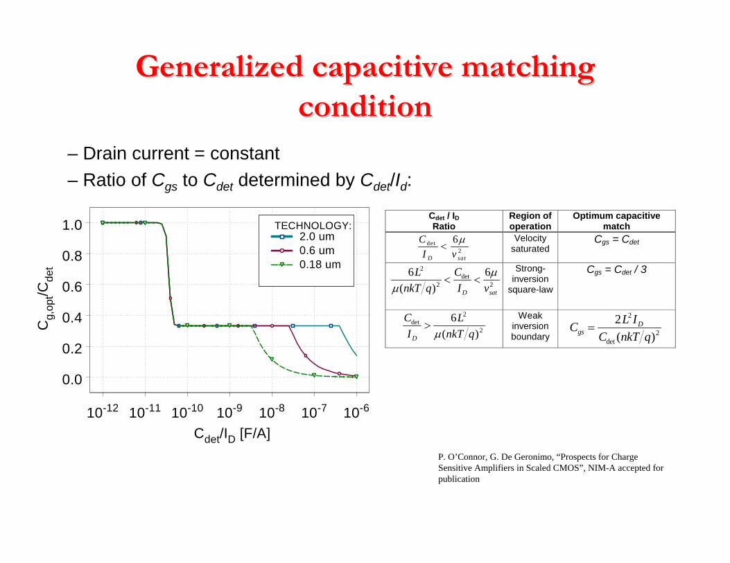
Generalized capacitive matching Generalized capacitive matching conditioncondition
10-12 10-11 10-10 10-9 10-8 10-7 10-6
Cdet/ID [F/A]
0.0
0.2
0.4
0.6
0.8
1.0
Cg,
opt/C
det
2.0 um0.6 um0.18 um
TECHNOLOGY:Cdet / ID Ratio
Region of operation
Optimum capacitive match
CI vD sat
det <6
2
µ
Velocity saturated
Cgs = Cdet
6 62
2 2
LnkT q
CI vD satµ
µ( )
det< <
Strong-inversion
square-law
Cgs = Cdet / 3
CI
LnkT qD
det
( )>
6 2
2µ Weak
inversion boundary
C L IC nkT qgs
D=2 2
2det ( )
– Drain current = constant– Ratio of Cgs to Cdet determined by Cdet/Id:
P. O’Connor, G. De Geronimo, “Prospects for Charge Sensitive Amplifiers in Scaled CMOS”, NIM-A accepted for publication
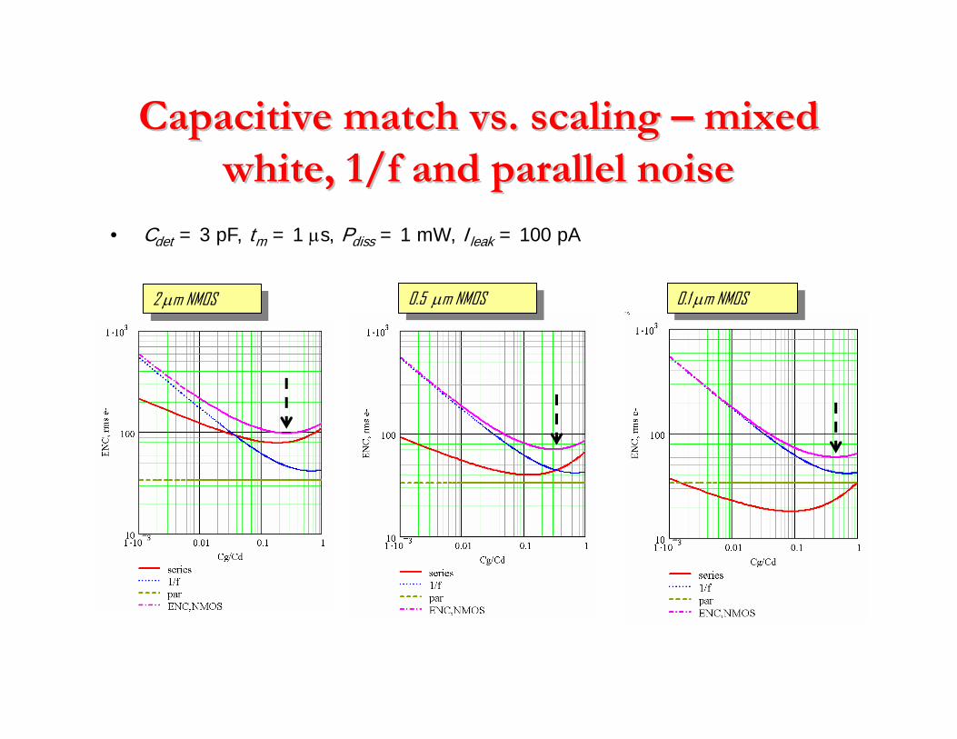
Capacitive match vs. scaling Capacitive match vs. scaling –– mixed mixed white, 1/f and parallel noisewhite, 1/f and parallel noise
• Cdet = 3 pF, tm = 1 µs, Pdiss = 1 mW, Ileak = 100 pA
2 µm NMOS2 µm NMOS 0.5 µm NMOS0.5 µm NMOS 0.1 µm NMOS0.1 µm NMOS
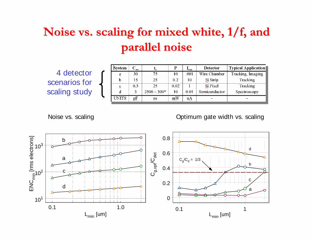
Noise vs. scaling for mixed white, 1/f, and Noise vs. scaling for mixed white, 1/f, and parallel noiseparallel noise
0.1 1.0Lmin [um]
101
102
103
ENC
min
[rm
s el
ectro
ns]
a
b
c
d
Noise vs. scaling Optimum gate width vs. scaling
4 detector scenarios for scaling study
b
a
c
0.1 1Lmin [um]
0
0.2
0.4
0.6
0.8
Cg,
opt/C
det
Cg/Cd = 1/3
d
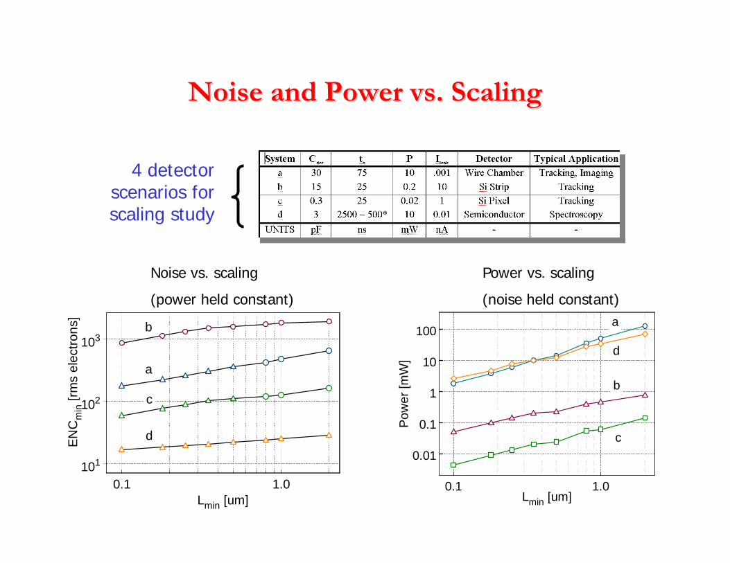
Noise and Power vs. ScalingNoise and Power vs. Scaling
0.1 1.0Lmin [um]
0.01
0.1
1
10
100
Pow
er [m
W]
d
a
b
c
0.1 1.0Lmin [um]
101
102
103
ENC
min
[rm
s el
ectro
ns]
a
b
c
d
Noise vs. scaling
(power held constant)
Power vs. scaling
(noise held constant)
4 detector scenarios for scaling study
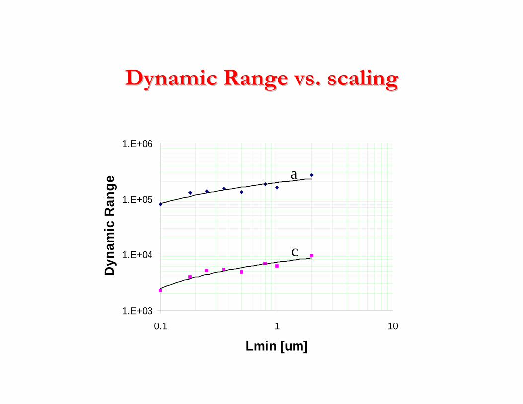
Dynamic Range vs. scalingDynamic Range vs. scaling
1.E+03
1.E+04
1.E+05
1.E+06
0.1 1 10
Lmin [um]
Dyn
amic
Ran
ge
a
c
InterconnectInterconnect
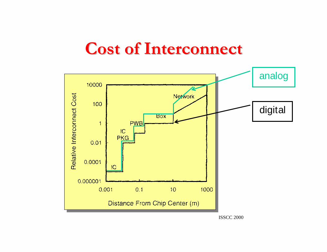
Cost of InterconnectCost of Interconnect
ISSCC 2000
digital
analog
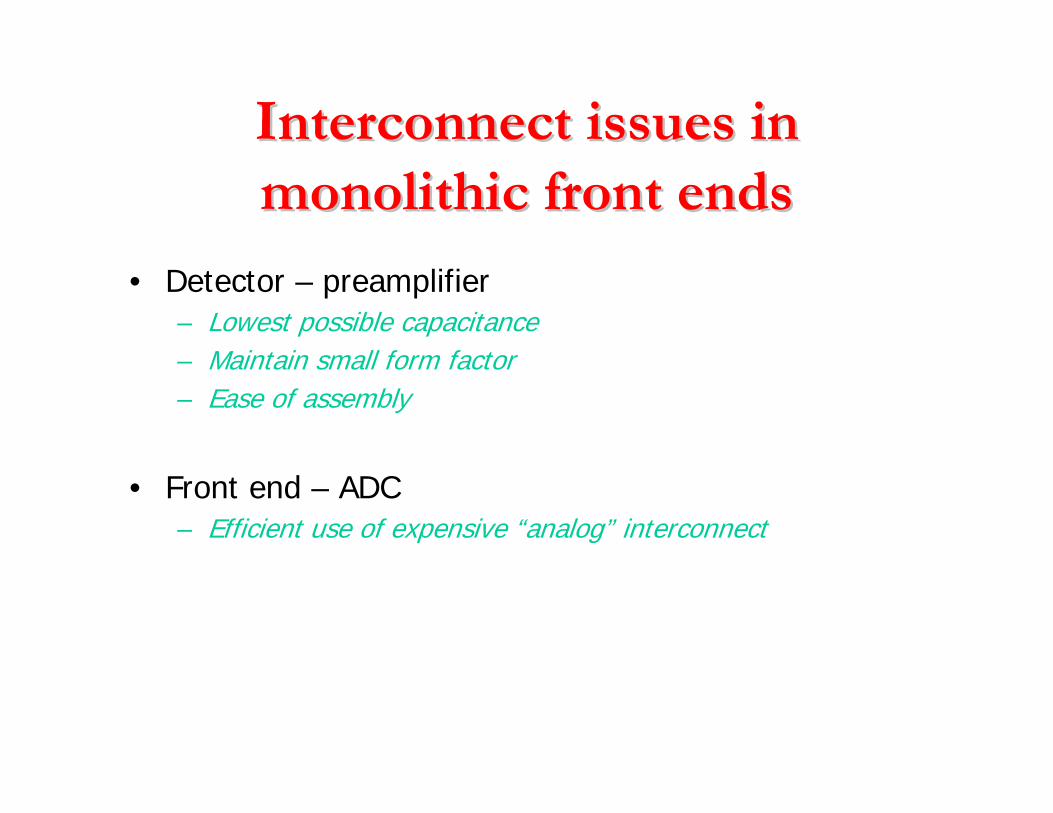
Interconnect issues in Interconnect issues in monolithic front endsmonolithic front ends
• Detector – preamplifier– Lowest possible capacitance– Maintain small form factor– Ease of assembly
• Front end – ADC– Efficient use of expensive “analog” interconnect
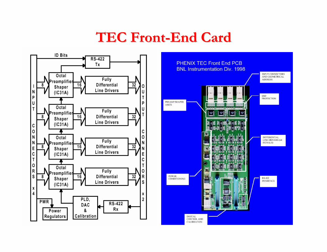
TEC FrontTEC Front--End CardEnd Card
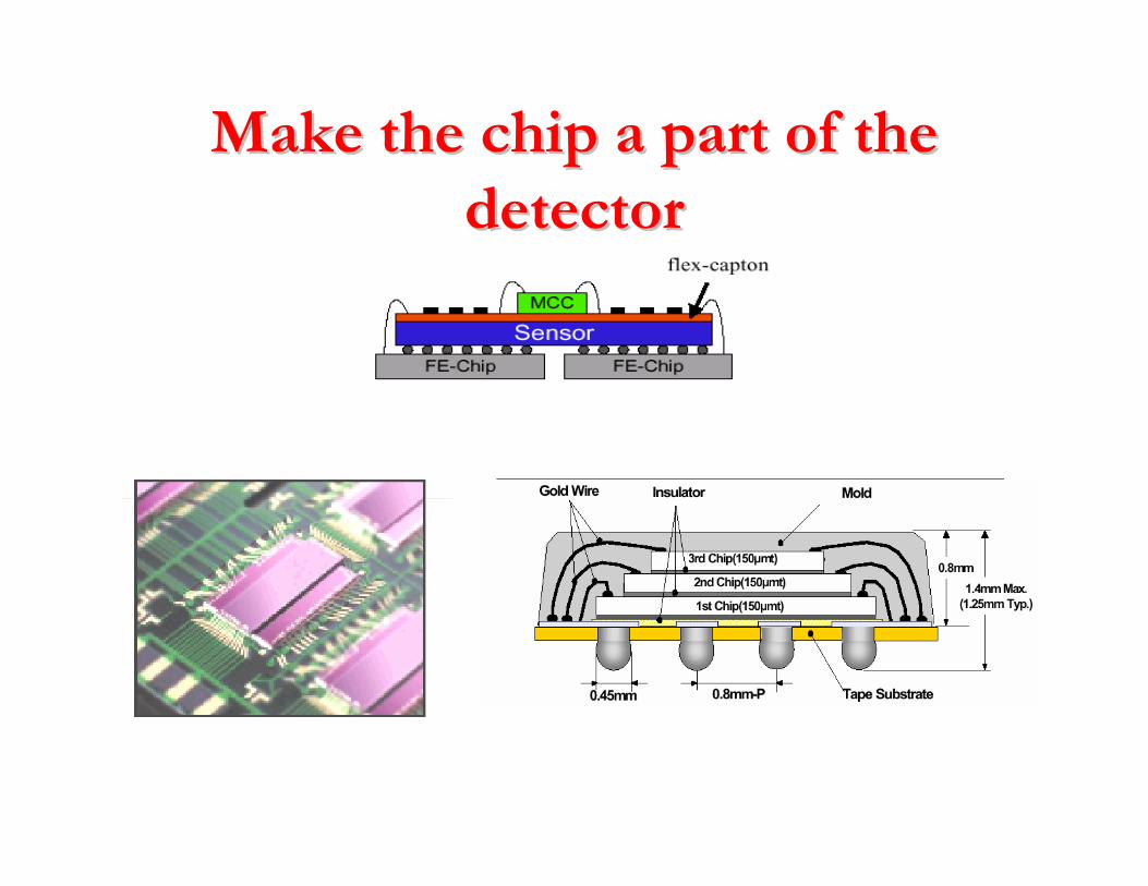
Make the chip a part of the Make the chip a part of the detectordetector
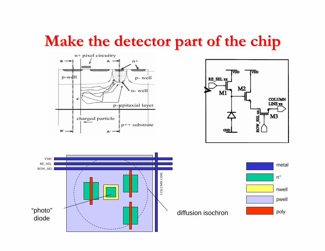
diffusion isochron“photo”diode
metal
n+
nwell
pwell
poly
Make the detector part of the chipMake the detector part of the chip
VDDRE_SEL
ROW_SEL
CO
LUM
N L
INE
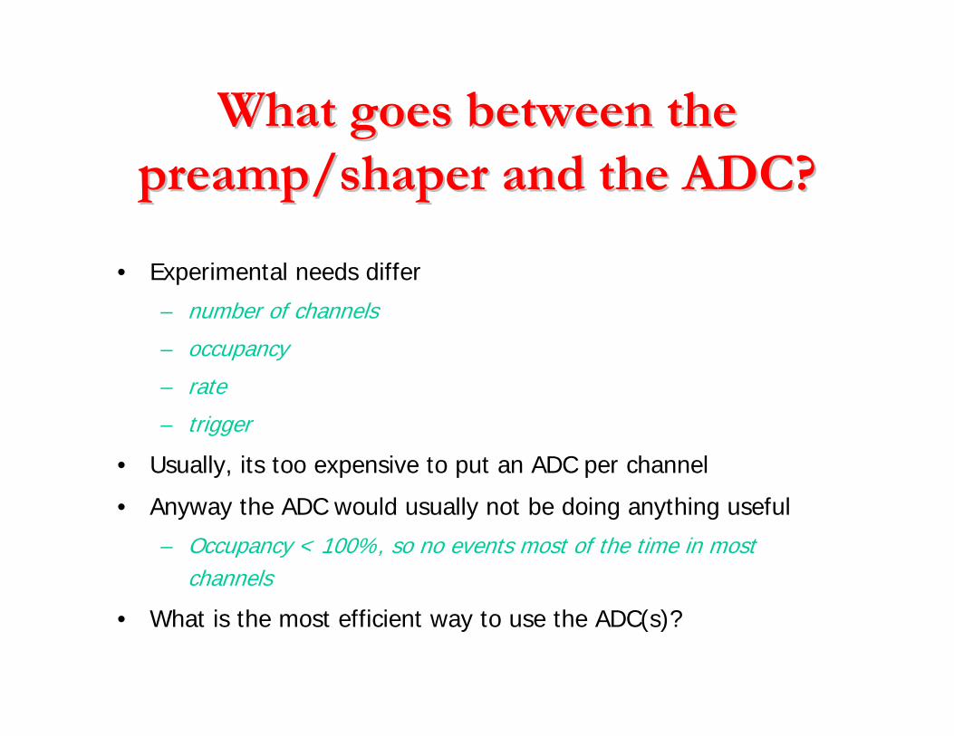
What goes between the What goes between the preamp/shaper and the ADC?preamp/shaper and the ADC?
• Experimental needs differ
– number of channels
– occupancy
– rate
– trigger
• Usually, its too expensive to put an ADC per channel
• Anyway the ADC would usually not be doing anything useful
– Occupancy < 100%, so no events most of the time in most channels
• What is the most efficient way to use the ADC(s)?
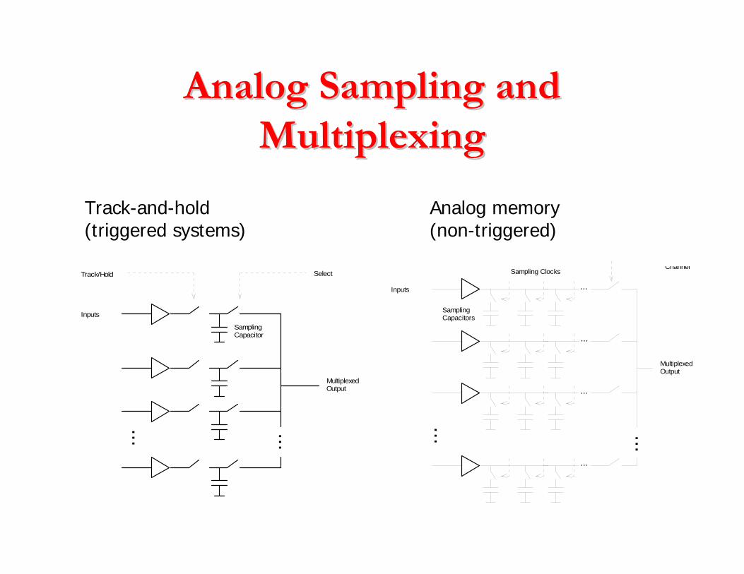
Analog Sampling and Analog Sampling and MultiplexingMultiplexing
Track/Hold
Inputs
Select
MultiplexedOutput
SamplingCapacitor
... ...Sampling Clocks
Inputs
Channel
MultiplexedOutput
SamplingCapacitors
... ...
...
...
...
...
Track-and-hold(triggered systems)
Analog memory(non-triggered)
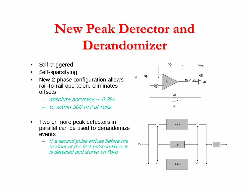
New Peak Detector and New Peak Detector and DerandomizerDerandomizer
• Self-triggered• Self-sparsifying• New 2-phase configuration allows
rail-to-rail operation, eliminates offsets– absolute accuracy ~ 0.2%– to within 300 mV of rails
• Two or more peak detectors in parallel can be used to derandomizeevents– If a second pulse arrives before the
readout of the first pulse in Pd-a, it is detected and stored on Pd-b.
S1
S3
M1
Vdd
Vout
Voff +
C
Vh
S2 VgVin
A-
+
Pd-a
Pd-b
LogicVin ADC
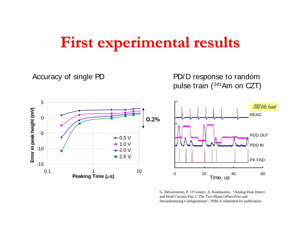
First experimental resultsFirst experimental results
0 20 40 60Time, us
READ
PDD OUT
PDD IN
PK FND
Accuracy of single PD PD/D response to randompulse train (241Am on CZT)
G. DeGeronimo, P. O’Connor, A. Kandasamy, “Analog Peak Detect and Hold Circuits Part 2: The Two-Phase Offset-Free and Derandomizing Configurations”, NIM-A submitted for publication
-15
-10
-5
0
5
0.1 1 10Peaking Time (µs)
Erro
r in
peak
hei
ght (
mV)
0.5 V1.0 V2.0 V2.5 V
0.2%
200 kHz fixed
Conclusions Conclusions • Today’s CMOS technology can be used to make low
noise front ends whose performance is nearly as good as the best discrete units
• In the future, increasing device cutoff frequency and gate oxide quality will help improve noise BUT– Potentially serious increases in 1/f noise and gate current
may accompany new process sequences– Low supply voltage will hamper high dynamic range
• Increasing attention will have to be paid to interconnect at the technology, circuit, and architecture levels