Generalized Reflection Coefficient, Smith Chart ...
44
M.H. Perrott High Speed Communication Circuits and Systems Lecture 4 Generalized Reflection Coefficient, Smith Chart, Integrated Passive Components Michael H. Perrott February 11, 2004 Copyright © 2004 by Michael H. Perrott All rights reserved. 1
Transcript of Generalized Reflection Coefficient, Smith Chart ...
M.H. Perrott
High Speed Communication Circuits and SystemsLecture 4
Generalized Reflection Coefficient, Smith Chart, Integrated Passive Components
Michael H. PerrottFebruary 11, 2004
Copyright © 2004 by Michael H. PerrottAll rights reserved.
1
M.H. PerrottM.H. Perrott
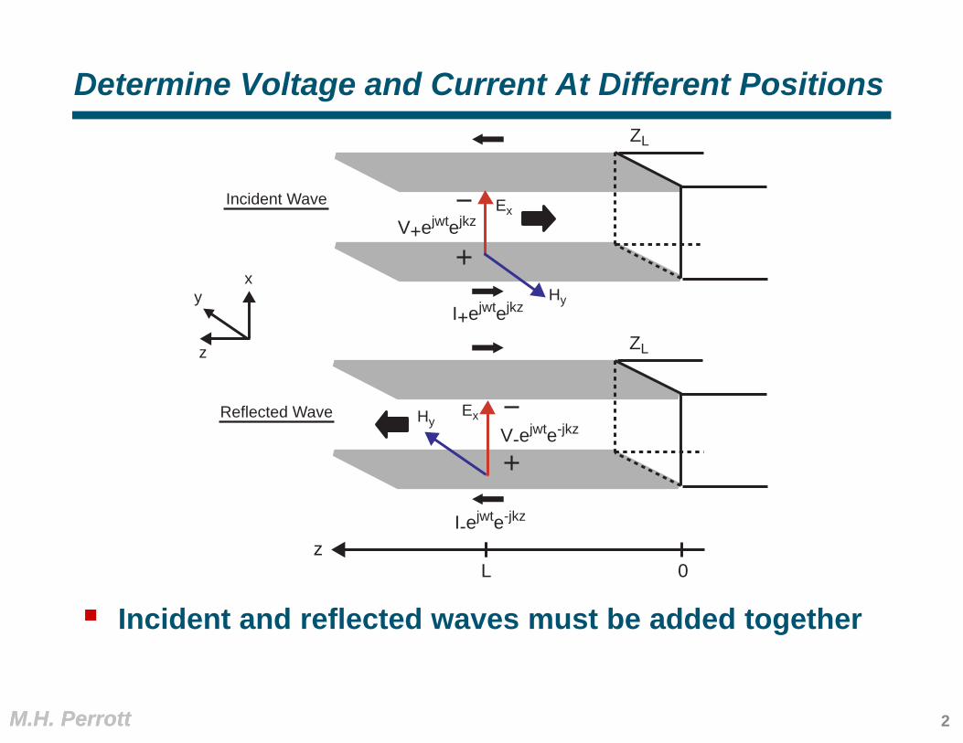
Determine Voltage and Current At Different Positions
Incident and reflected waves must be added together
x
z
Ex
Hyy
ZL
ExHy
ZL
Incident Wave
Reflected Wave
0Lz
V+ejwtejkz
I+ejwtejkz
V-ejwte-jkz
I-ejwte-jkz
2
M.H. PerrottM.H. Perrott
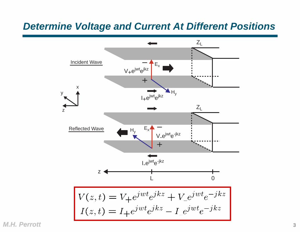
Determine Voltage and Current At Different Positions
x
z
Ex
Hyy
ZL
ExHy
ZL
Incident Wave
Reflected Wave
0Lz
V+ejwtejkz
I+ejwtejkz
V-ejwte-jkz
I-ejwte-jkz
3

M.H. PerrottM.H. Perrott
Define Generalized Reflection Coefficient
Similarly:
4
M.H. PerrottM.H. Perrott
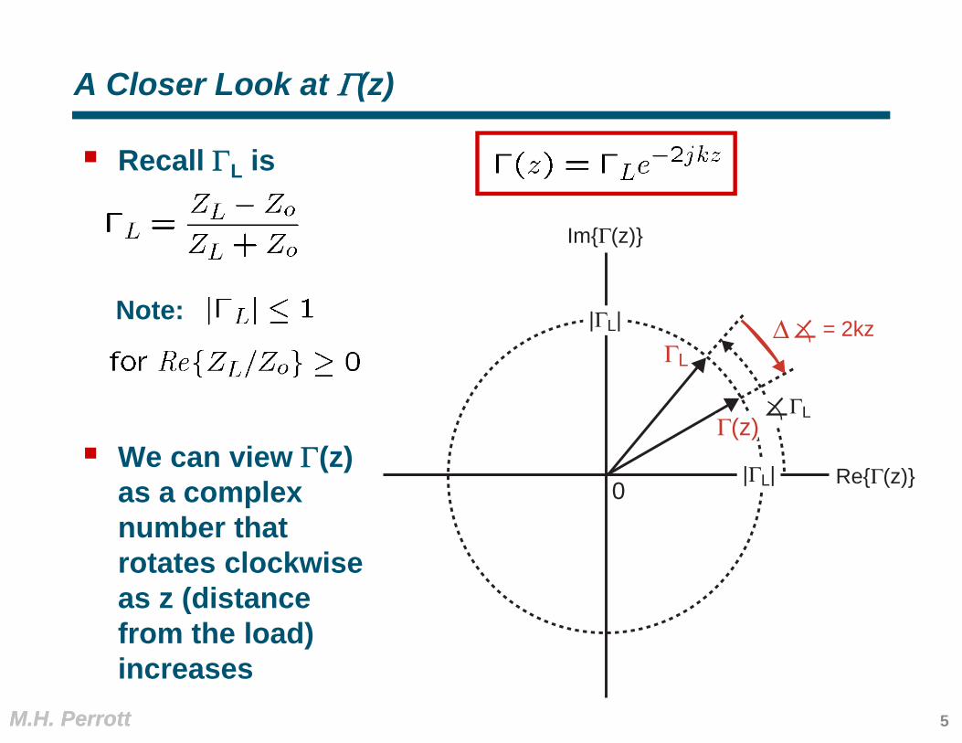
A Closer Look at (z)
Recall L is
We can view (z) as a complex number that rotates clockwise as z (distance from the load) increases
Note: |ΓL|
|ΓL| Re{Γ(z)}
Im{Γ(z)}
ΓL
Δ = 2kzΓL
Γ(z)
0
5

M.H. PerrottM.H. Perrott
Calculate |Vmax| and |Vmin| Across The Transmission Line
We found that
So that the max and min of V(z,t) are calculated as
We can calculate this geometrically!
6

M.H. PerrottM.H. Perrott
A Geometric View of |1 + (z)|
|ΓL|
Re{1+Γ(z)}
Im{1+Γ(z)}
Γ(z)
10
|1+Γ(z)|
7

M.H. PerrottM.H. Perrott
Reflections Cause Amplitude to Vary Across Line
Equation: Graphical representation:
directionof travel
z
tV+ejwtejkz
z
|1 + Γ(z)|
max|1+Γ(z)|
λ
0
min|1+Γ(z)|
|1+Γ(0)|
8
M.H. PerrottM.H. Perrott
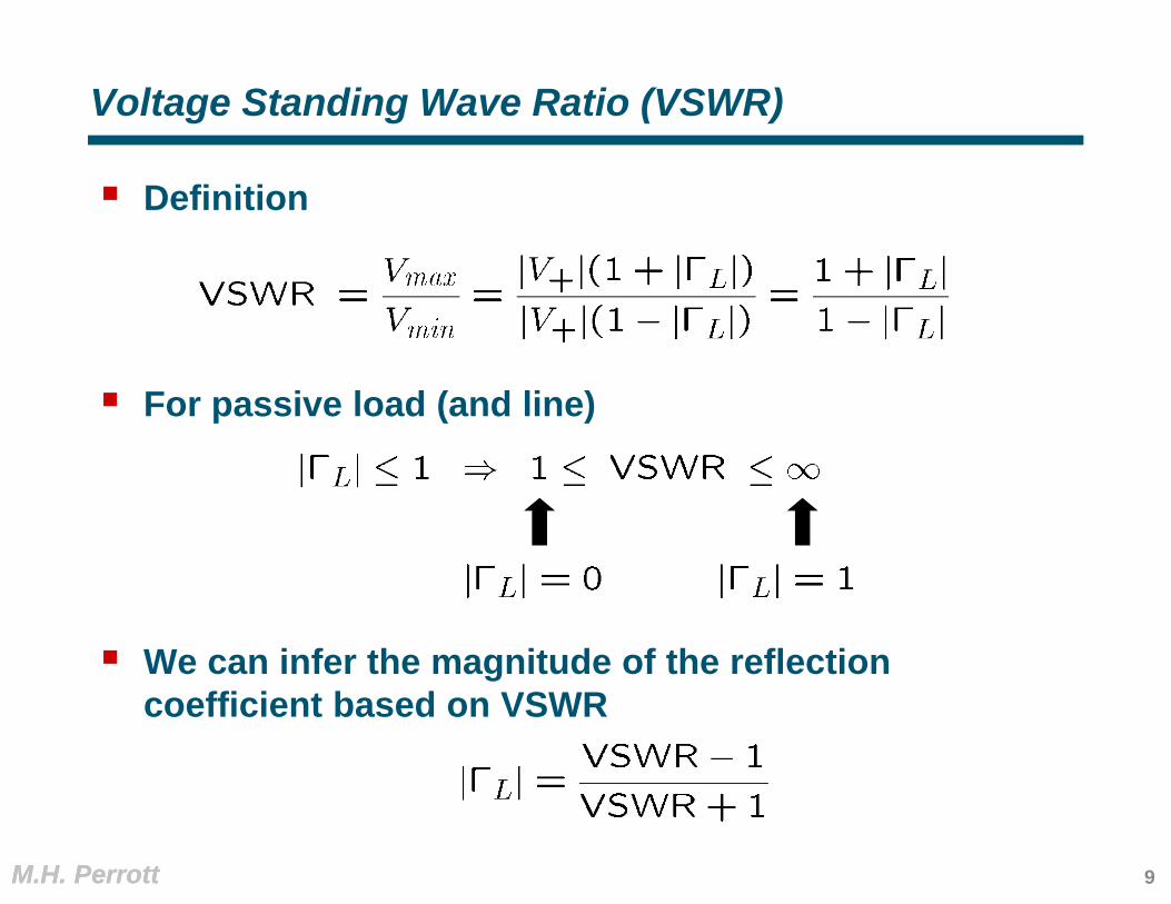
Voltage Standing Wave Ratio (VSWR)
Definition
For passive load (and line)
We can infer the magnitude of the reflection coefficient based on VSWR
9
M.H. PerrottM.H. Perrott
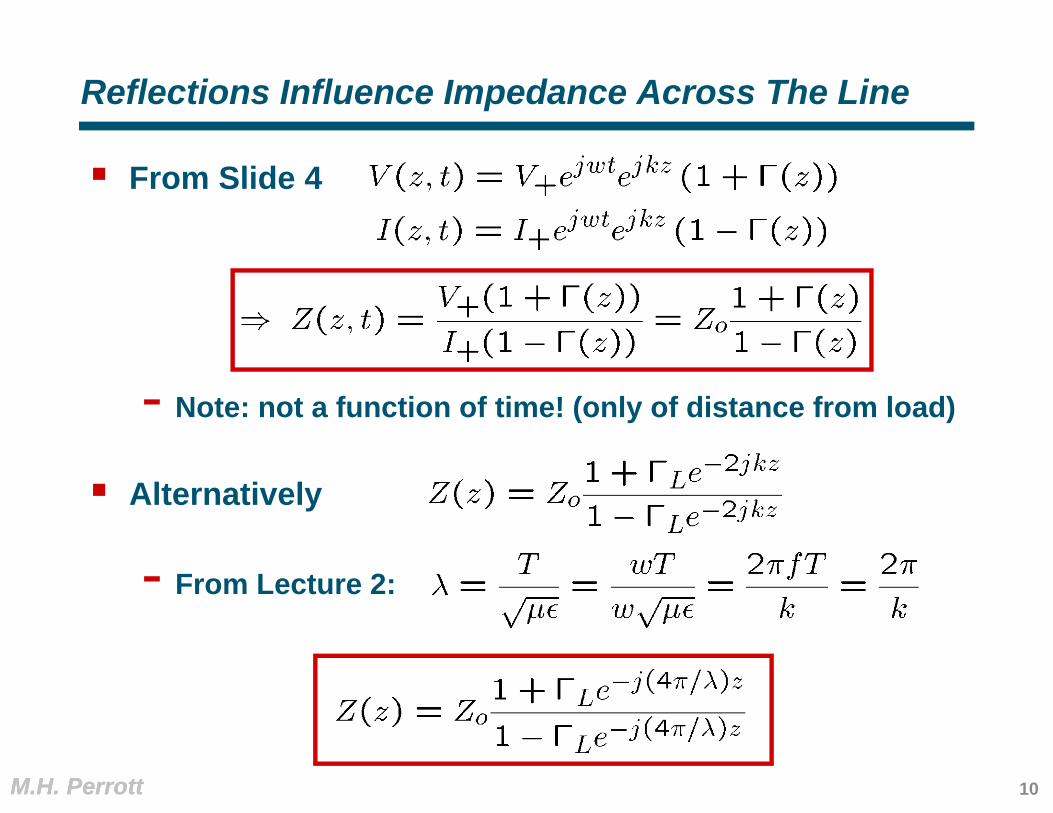
Reflections Influence Impedance Across The Line
From Slide 4
- Note: not a function of time! (only of distance from load)
Alternatively
- From Lecture 2:
10

M.H. PerrottM.H. Perrott
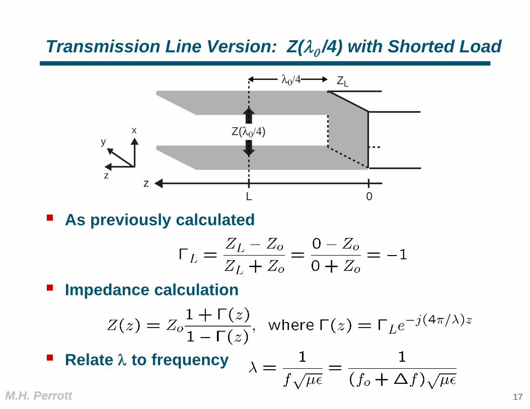
Example: Z(/4) with Shorted Load
Calculate reflection coefficient
Calculate generalized reflection coefficient
Calculate impedance
x
z
y
ZL
0Lz
λ/4
Z(λ/4)
11
M.H. PerrottM.H. Perrott
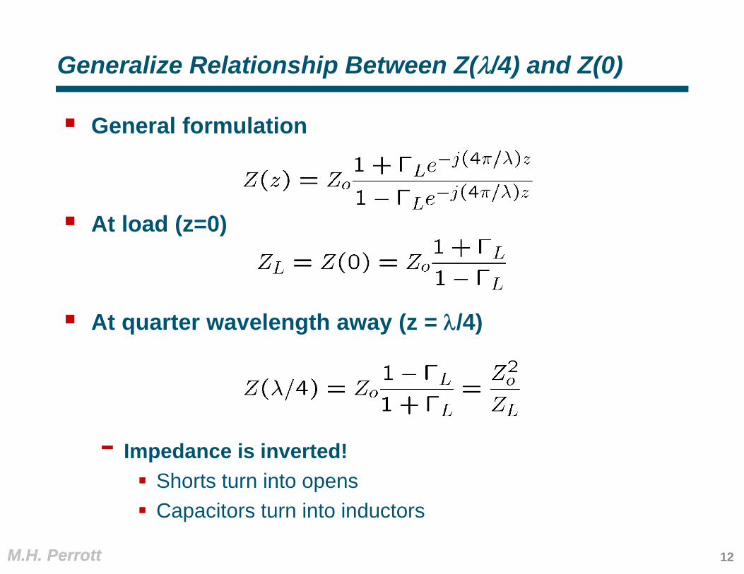
Generalize Relationship Between Z(/4) and Z(0)
General formulation
At load (z=0)
At quarter wavelength away (z = /4)
- Impedance is inverted! Shorts turn into opens Capacitors turn into inductors
12

M.H. PerrottM.H. Perrott
Now Look At Z() (Impedance Close to Load)
Impedance formula ( very small)
- A useful approximation:
- Recall from Lecture 2:
Overall approximation:
13
M.H. PerrottM.H. Perrott
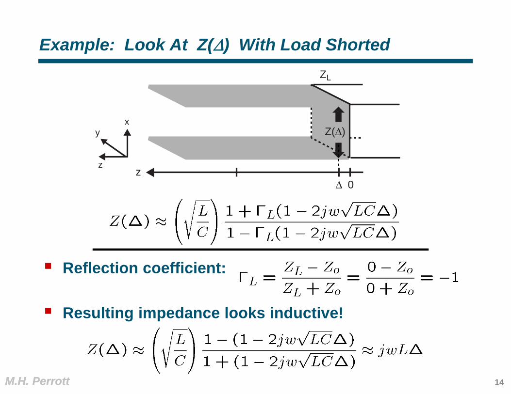
Example: Look At Z() With Load Shorted
Reflection coefficient:
Resulting impedance looks inductive!
x
z
y
ZL
0Δz
Z(Δ)
14
M.H. PerrottM.H. Perrott
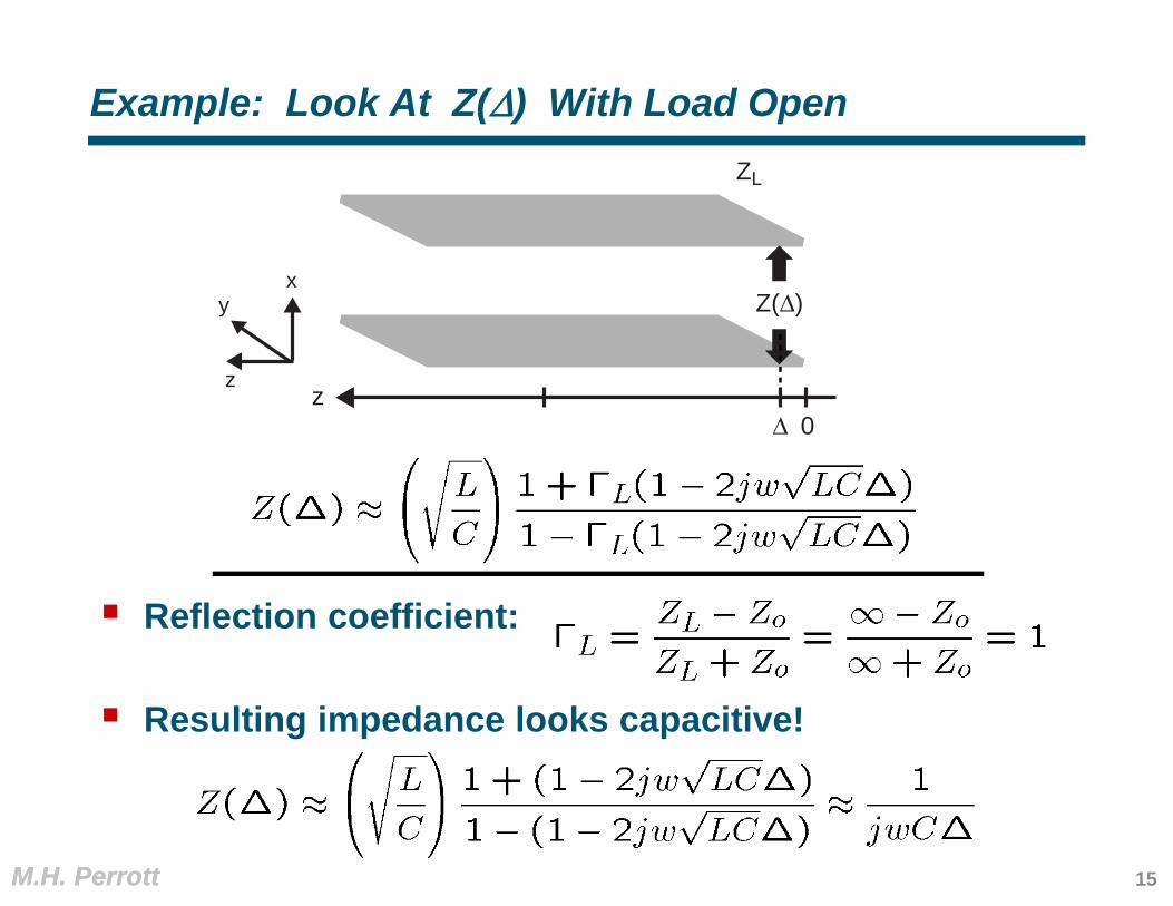
Example: Look At Z() With Load Open
Reflection coefficient:
Resulting impedance looks capacitive!
x
z
y
ZL
0Δz
Z(Δ)
15
M.H. PerrottM.H. Perrott
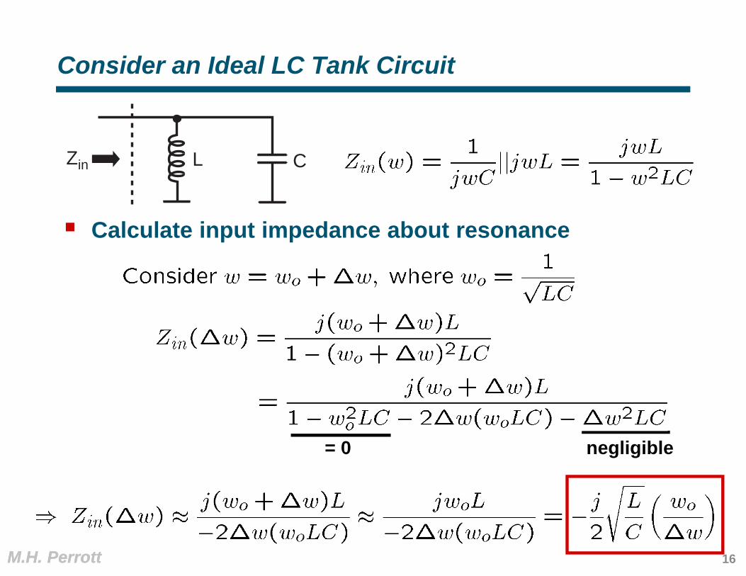
Consider an Ideal LC Tank Circuit
Calculate input impedance about resonance
L CZin
= 0 negligible
16
M.H. PerrottM.H. Perrott
Transmission Line Version: Z(/4) with Shorted Load
As previously calculated
Impedance calculation
Relate to frequency
x
z
y
ZL
0Lz
λ0/4
Z(λ0/4)
17
M.H. PerrottM.H. Perrott
Calculate Z( f) – Step 1
Wavelength as a function of f
Generalized reflection coefficient
x
z
y
ZL
0Lz
λ0/4
Z(λ0/4)
18

M.H. PerrottM.H. Perrott
Calculate Z( f) – Step 2
Impedance calculation
Recall
x
z
y
ZL
0Lz
λ0/4
Z(λ0/4)
- Looks like LC tank circuit (but more than one mode)!19
M.H. PerrottM.H. Perrott
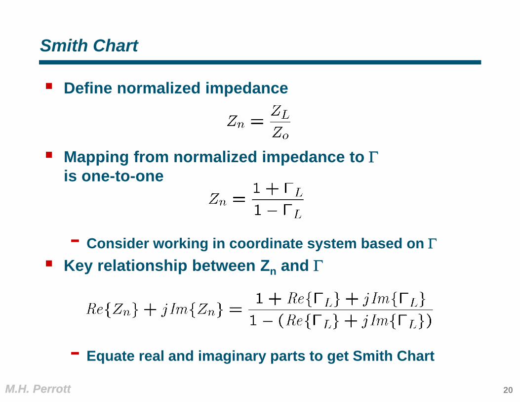
Smith Chart
Define normalized impedance
Mapping from normalized impedance to is one-to-one
- Consider working in coordinate system based on Key relationship between Zn and
- Equate real and imaginary parts to get Smith Chart
20

M.H. PerrottM.H. Perrott
Real Impedance in Coordinates (Equate Real Parts)
0.2 0.5 1 2 5
ΓL=0
Im{ΓL}
Re{ΓL}
ΓL=1ΓL=-1
ΓL=j
ΓL=-j
Zn=0.5
21
M.H. PerrottM.H. Perrott
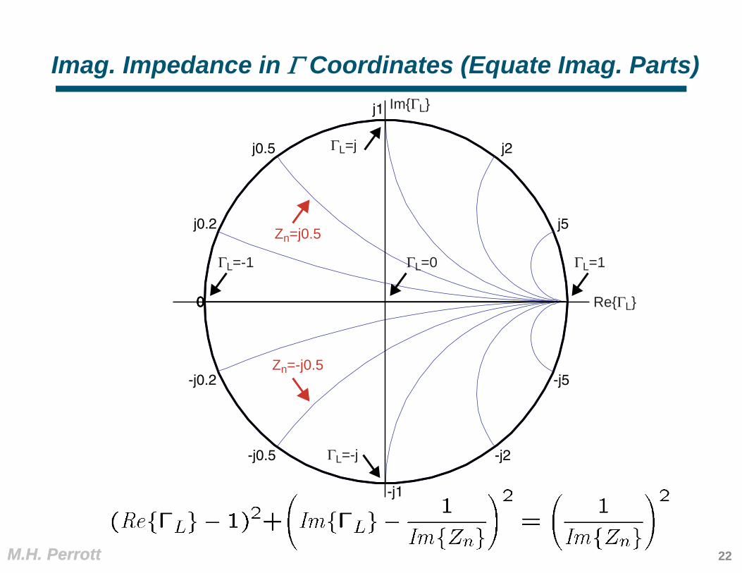
Imag. Impedance in Coordinates (Equate Imag. Parts)
j0.2
-j0.2
0
j0.5
-j0.5
0
j1
-j1
0
j2
-j2
0
j5
-j5
0
Im{ΓL}
Re{ΓL}
ΓL=0 ΓL=1ΓL=-1
ΓL=j
ΓL=-j
Zn=j0.5
Zn=-j0.5
22

M.H. PerrottM.H. Perrott
What Happens When We Invert the Impedance?
Fundamental formulas
Impact of inverting the impedance
- Derivation:
We can invert complex impedances in plane by simply changing the sign of !
How can we best exploit this?
23
M.H. PerrottM.H. Perrott
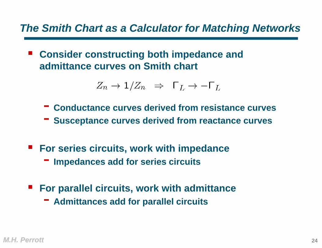
The Smith Chart as a Calculator for Matching Networks
Consider constructing both impedance and admittance curves on Smith chart
- Conductance curves derived from resistance curves- Susceptance curves derived from reactance curves
For series circuits, work with impedance- Impedances add for series circuits
For parallel circuits, work with admittance- Admittances add for parallel circuits
24

M.H. PerrottM.H. Perrott
Resistance and Conductance on the Smith Chart
0.2 0.5 1 2 5
Im{ΓL}
Re{ΓL}
ΓL=0 ΓL=1ΓL=-1
ΓL=j
ΓL=-j
Yn=2
Yn=0.5 Zn=0.5
Zn=2
25

M.H. PerrottM.H. Perrott
Reactance and Susceptance on the Smith Chart
j0.2
-j0.2
0
j0.5
-j0.5
0
j1
-j1
0
j2
-j2
0
j5
-j5
0
Im{ΓL}
Re{ΓL}
ΓL=0 ΓL=1ΓL=-1
ΓL=j
ΓL=-j
Yn=-j2
Yn=j2
Zn=j2
Zn=-j2
26
M.H. PerrottM.H. Perrott
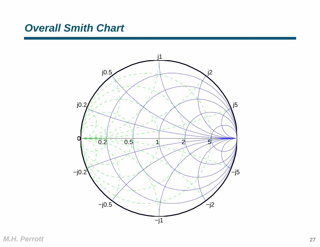
Overall Smith Chart
0.2 0.5 1 2 5
j0.2
−j0.2
0
j0.5
−j0.5
0
j1
−j1
0
j2
−j2
0
j5
−j5
0
27

M.H. PerrottM.H. Perrott
Example – Match RC Network to 50 Ohms at 2.5 GHz
Circuit
Step 1: Calculate ZLn
Step 2: Plot ZLn on Smith Chart (use admittance, YLn)
Zin Rp=200Cp=1pFMatchingNetwork ZL
28

M.H. PerrottM.H. Perrott
Plot Starting Impedance (Admittance) on Smith Chart
0.2 0.5 1 2 5
j0.2
-j0.2
0
j0.5
-j0.5
0
j1
-j1
0
j2
-j2
0
j5
-j5
0
YLn=0.25+j0.7854
(Note: ZLn=0.37-j1.16)
29
M.H. PerrottM.H. Perrott
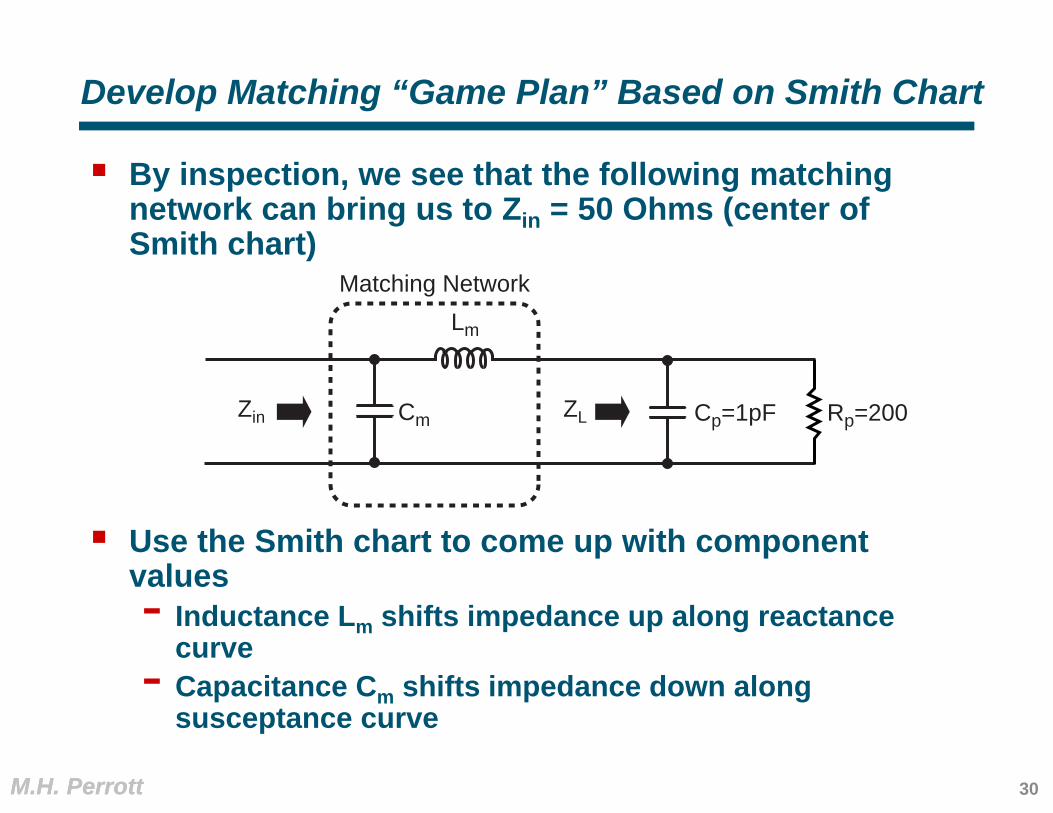
Develop Matching “Game Plan” Based on Smith Chart
By inspection, we see that the following matching network can bring us to Zin = 50 Ohms (center of Smith chart)
Use the Smith chart to come up with component values- Inductance Lm shifts impedance up along reactance
curve- Capacitance Cm shifts impedance down along susceptance curve
Zin Rp=200Cp=1pFZL
Lm
Cm
Matching Network
30

M.H. PerrottM.H. Perrott
Add Reactance of Inductor Lm
0.2 0.5 1 2 5
j0.2
-j0.2
0
j0.5
-j0.5
0
j1
-j1
0
j2
-j2
0
j5
-j5
0
ZLn=0.37-j1.16
Z2n=0.37+j0.48
normalizedinductor
reactance= j1.64
31

M.H. PerrottM.H. Perrott
Inductor Value Calculation Using Smith Chart
From Smith chart, we found that the desired normalized inductor reactance is
Required inductor value is therefore
32
M.H. PerrottM.H. Perrott
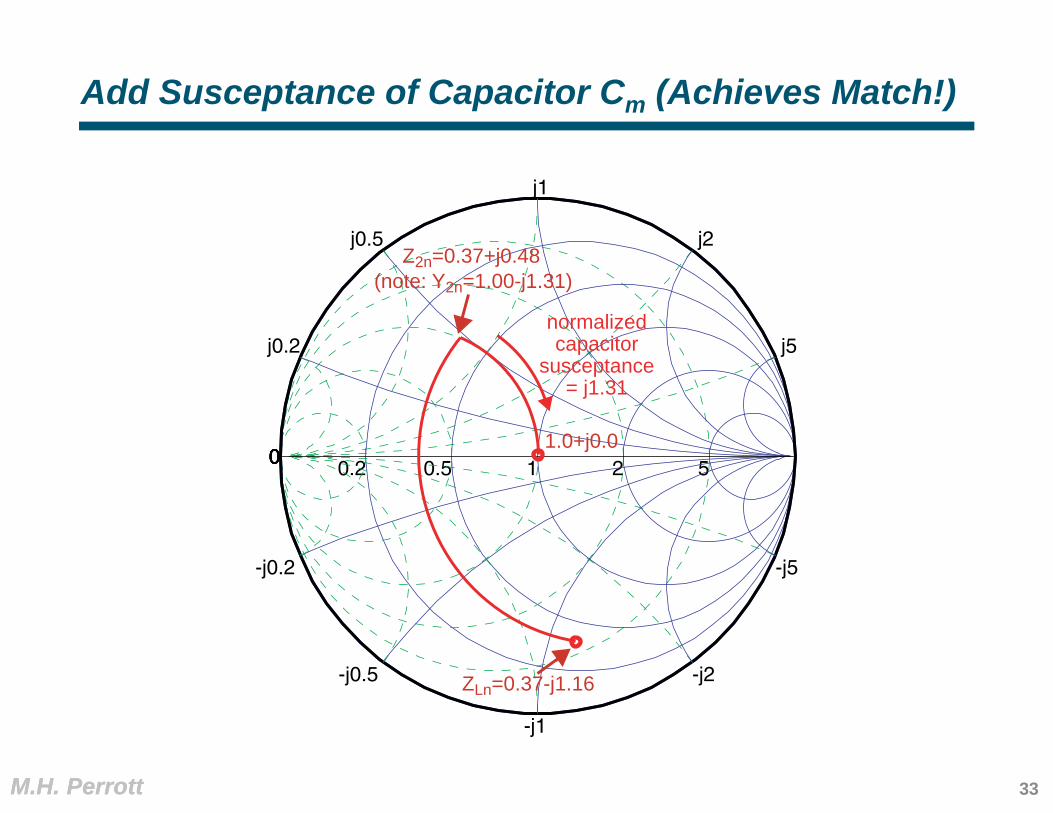
Add Susceptance of Capacitor Cm (Achieves Match!)
0.2 0.5 1 2 5
j0.2
-j0.2
0
j0.5
-j0.5
0
j1
-j1
0
j2
-j2
0
j5
-j5
0
ZLn=0.37-j1.16
Z2n=0.37+j0.48
1.0+j0.0
normalizedcapacitor
susceptance= j1.31
(note: Y2n=1.00-j1.31)
33
M.H. PerrottM.H. Perrott
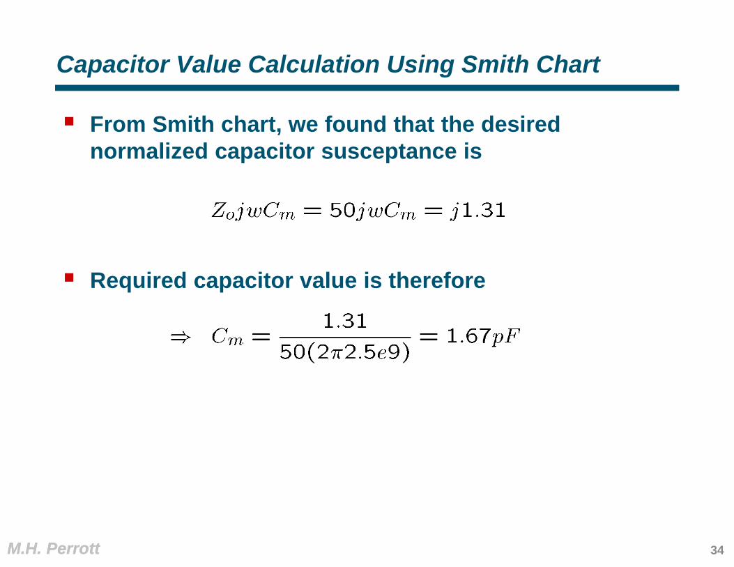
Capacitor Value Calculation Using Smith Chart
From Smith chart, we found that the desired normalized capacitor susceptance is
Required capacitor value is therefore
34
M.H. PerrottM.H. Perrott
Just For Fun
Play the “matching game” at
- Allows you to graphically tune several matching networks- Note: game is set up to match source to load impedance
rather than match the load to the source impedance Same results, just different viewpoint
http://contact.tm.agilent.com/Agilent/tmo/an-95-1/classes/imatch.html
35
M.H. Perrott
Passives
36
M.H. PerrottM.H. Perrott
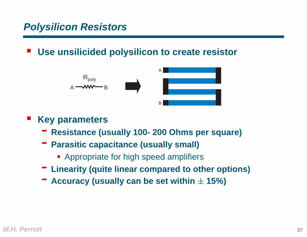
Polysilicon Resistors
Use unsilicided polysilicon to create resistor
Key parameters- Resistance (usually 100- 200 Ohms per square)- Parasitic capacitance (usually small)
Appropriate for high speed amplifiers- Linearity (quite linear compared to other options)- Accuracy (usually can be set within ± 15%)
A
Rpoly
B
B
A
37

M.H. PerrottM.H. Perrott
MOS Resistors
Bias a MOS device in its triode region
High resistance values can be achieved in a small area (MegaOhms within tens of square microns)
Resistance is quite nonlinear- Appropriate for small swing circuits
AW/LRds
B A B
38

M.H. PerrottM.H. Perrott
High Density Capacitors (Biasing, Decoupling)
MOS devices offer the highest capacitance per unit area- Limited to a one terminal device- Voltage must be high enough to invert the channel
Key parameters- Capacitance value
Raw cap value from MOS device is 6.1 fF/ m2 for 0.24u CMOS
- Q (i.e., amount of series resistance) Maximized with minimum L (tradeoff with area efficiency)
See pages 39-40 of Tom Lee’s book
A
W/L
A
C1=CoxWL
39
M.H. PerrottM.H. Perrott
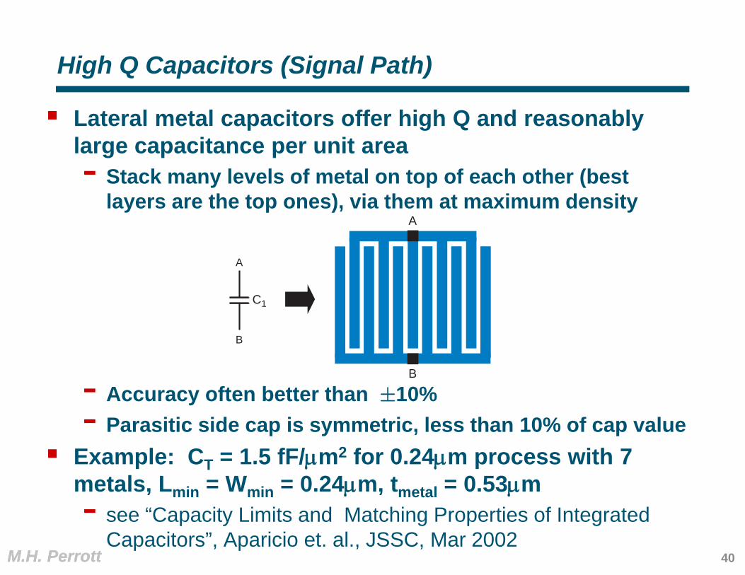
High Q Capacitors (Signal Path)
Lateral metal capacitors offer high Q and reasonably large capacitance per unit area- Stack many levels of metal on top of each other (best
layers are the top ones), via them at maximum density
- Accuracy often better than ±10%- Parasitic side cap is symmetric, less than 10% of cap value
Example: CT = 1.5 fF/m2 for 0.24m process with 7 metals, Lmin = Wmin = 0.24m, tmetal = 0.53m- see “Capacity Limits and Matching Properties of Integrated
Capacitors”, Aparicio et. al., JSSC, Mar 2002
B
A
C1
A
B
40
M.H. PerrottM.H. Perrott
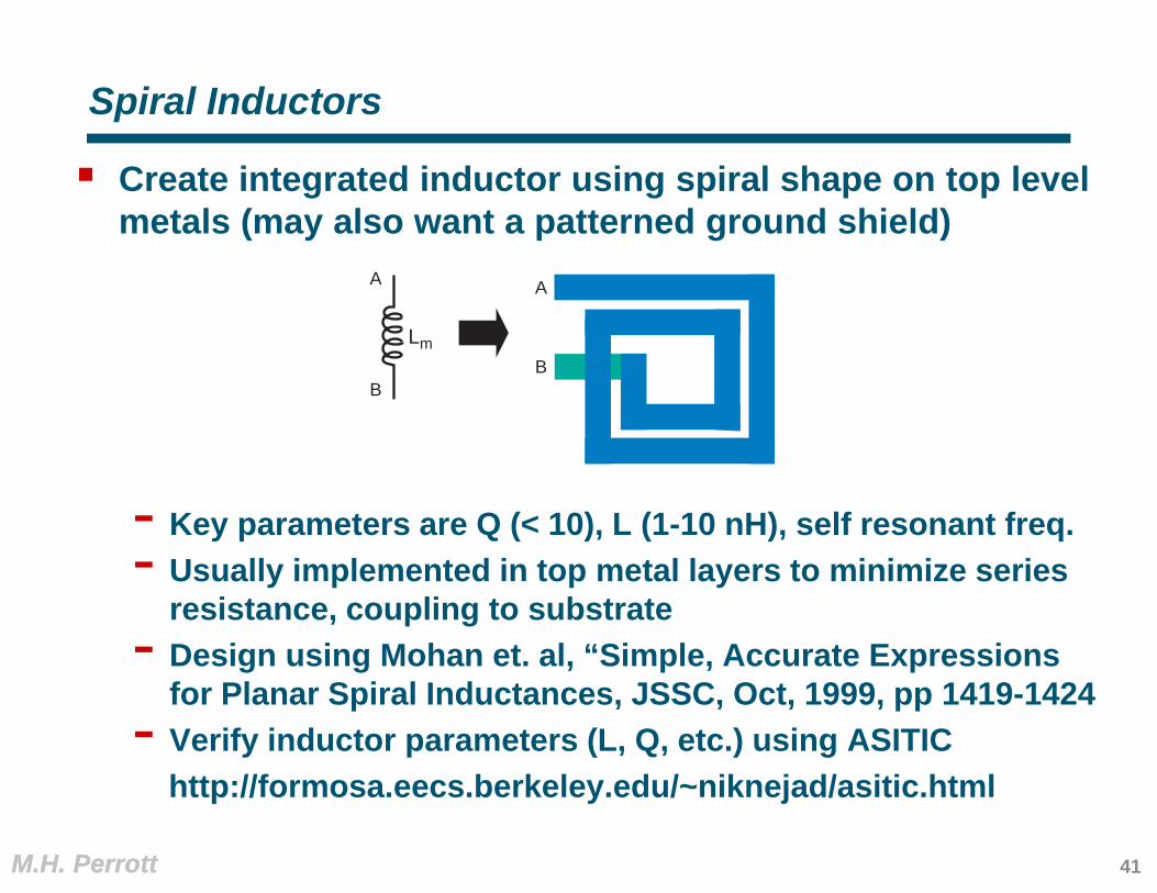
Spiral Inductors
Create integrated inductor using spiral shape on top level metals (may also want a patterned ground shield)
- Key parameters are Q (< 10), L (1-10 nH), self resonant freq.- Usually implemented in top metal layers to minimize series
resistance, coupling to substrate- Design using Mohan et. al, “Simple, Accurate Expressions
for Planar Spiral Inductances, JSSC, Oct, 1999, pp 1419-1424- Verify inductor parameters (L, Q, etc.) using ASITIC
http://formosa.eecs.berkeley.edu/~niknejad/asitic.html
Lm
A
BB
A
41
M.H. PerrottM.H. Perrott
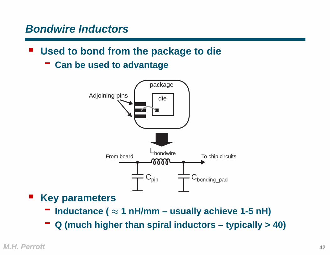
Bondwire Inductors
Used to bond from the package to die- Can be used to advantage
Key parameters- Inductance ( ≈ 1 nH/mm – usually achieve 1-5 nH)- Q (much higher than spiral inductors – typically > 40)
Cpin
Lbondwire
Cbonding_pad
dieAdjoining pins
package
To chip circuitsFrom board
42

M.H. PerrottM.H. Perrott
Integrated Transformers
Utilize magnetic coupling between adjoining wires
Key parameters- L (self inductance for primary and secondary windings)- k (coupling coefficient between primary and secondary)
Design – ASITIC, other CAD packages
A B
L2
B
L1
A
Cpar1
k C D
C DCpar2
43
M.H. PerrottM.H. Perrott
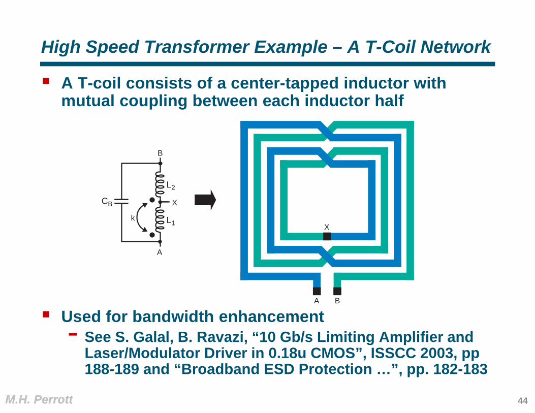
High Speed Transformer Example – A T-Coil Network
A T-coil consists of a center-tapped inductor with mutual coupling between each inductor half
Used for bandwidth enhancement- See S. Galal, B. Ravazi, “10 Gb/s Limiting Amplifier and Laser/Modulator Driver in 0.18u CMOS”, ISSCC 2003, pp 188-189 and “Broadband ESD Protection …”, pp. 182-183
A B
X
L2
B
L1
A
CB X
k
44